Note: Descriptions are shown in the official language in which they were submitted.
I
SOLID STATE LIGHTING DEVICES WITH REDUCED MELATONIN
SUPPRESSION CHARACTERISTICS
CROSS-REFERENCE TO RELATED APPLICATIONS
[0001] This application claims priority to U.S. Patent Application No.
15/994,483 filed on May 31, 2018.
Field of the Disclosure
[0002] The present disclosure relates to solid state lighting devices,
including
devices with lumiphors arranged to be stimulated by electrically activated
solid
state emitters, and relates to associated methods of making and using such
devices.
Background
[0003] Solid state lighting devices such as light-emitting diodes (LEDs)
are
increasingly used in both consumer and commercial applications. Advancements
in LED technology have resulted in highly efficient and mechanically robust
light
sources with a long service life. Accordingly, modern LEDs have enabled a
variety of new display applications and are increasingly utilized for general
illumination applications, often replacing incandescent and fluorescent light
sources.
[0004] LEDs are solid state devices that convert electrical energy to
light and
generally include one or more active layers of semiconductor material (or an
active region) arranged between oppositely doped n-type and p-type layers.
When a bias is applied across the doped layers, holes and electrons are
injected
into the one or more active layers where they recombine to generate emissions
such as visible light or ultraviolet (UV) emissions or infrared (IR)
emissions. A
LED chip typically includes an active region that may be fabricated, for
example,
from silicon carbide, gallium nitride, gallium phosphide, aluminum nitride,
gallium
arsenide-based materials, and/or from organic semiconductor materials.
[0005] Solid state emitters may include lumiphoric materials (also known
as
lumiphors) that absorb a portion of emissions having a first peak wavelength
emitted by the emitter and re-emit light having a second peak wavelength that
differs from the first peak wavelength. Phosphors, scintillators, and
lumiphoric
Date Recue/Date Received 2022-04-27
CA 03101735 2020-11-26
WO 2019/231711
PCT/US2019/032776
2
inks are common lumiphoric materials. Light perceived as white or near-white
may be generated by a combination of red, green, and blue (RGB) emitters, or,
alternatively, by combined emissions of a blue LED and a lunniphor such as a
yellow phosphor (e.g., YAG:Ce or Ce:YAG). In the latter case, a portion of the
blue LED emissions pass through the phosphor, while another portion of the
blue
emissions is downconverted to yellow, and the blue and yellow light in
combination are perceived as white. White light may also be produced by
stimulating phosphors or dyes of multiple colors with a violet or UV LED
source.
[0006] Emissions of a blue LED in combination with a yellow or green
lumiphoric material may be near-white in character and referred to as "blue-
shifted yellow" ("BSY") light or "blue-shifted green" (SSG") light. Addition
of red
(or red-orange) spectral output from a red-emitting LED (to yield a "BSY+R"
device) or from a red lumiphoric material (to yield a "BS(Y+R)" device) may be
used to increase the warmth of the aggregated light output and better
approximate light produced by incandescent lamps.
[0007] Color reproduction is commonly measured using color rendering
index
(CRI) or average color rendering index (CRI Ra). To calculate the CRI, the
color
appearance of 14 reflective samples is simulated when illuminated by a
reference
radiator (illuminant) and the test source. The CRI Ra is a modified average
utilizing the first eight indices, all of which have low to moderate chromatic
saturation. (R9 is one of six saturated test colors not used in calculating
CRI,
with R9 embodying a large red content.) The CRI and CRI Ra are used to
determine how closely an artificial light source matches the color rendering
of a
natural light source at the same correlated color temperature (CCT). Daylight
has a high CRI Ra (approximately 100), with incandescent bulbs also being
relatively close (CRI Ra greater than 95), and fluorescent lighting being less
accurate (with typical CRI Ra values of approximately 70-80).
[0008] The reference spectra used in color rendering index calculations
were
chosen as ideal illumination sources defined in terms of their color
temperature.
As a heated object becomes incandescent, it first glows reddish, then
yellowish,
then white, and finally bluish. Thus, apparent colors of incandescing
materials are
directly related to their actual temperature (in Kelvin (K)). Practical
materials that
incandesce are said to have CCT values that are directly related to color
temperatures of blackbody sources.
CA 03101735 2020-11-26
WO 2019/231711
PCT/US2019/032776
3
[0009] Aspects relating to the inventive subject matter disclosed herein
may
be better understood with reference to the 1931 CIE (Commission International
de l'Eclairage) Chromaticity Diagram, which is well-known and of which a copy
is
reproduced in FIG. 1. The 1931 CIE Chromaticity Diagram maps out the human
color perception in terms of two CIE parameters x and y. The spectral colors
are
distributed around the edge of the outlined space, which includes all of the
hues
perceived by the human eye. The boundary line represents maximum saturation
for the spectral colors. The chromaticity coordinates (i.e., color points)
that lie
along the blackbody locus (BBL) (also known as the Planckian locus) obey
Planck's equation: E(A)=A A-5/(eB1T-1), where E is the emission intensity, A
is the
emission wavelength, T is the color temperature of the blackbody, and A and B
are constants. Color coordinates that lie on or near the BBL (which embodies a
curved line emanating from the right lower corner) yield pleasing white light
to a
human observer. The 1931 CIE Diagram includes temperature listings along the
BBL, with these temperature listings showing the color path of a blackbody
radiator that is caused to increase to such temperatures. As a heated object
becomes incandescent, it first glows reddish, then yellowish, then white, and
finally bluish. This occurs because the wavelength associated with the peak
radiation of the blackbody radiator becomes progressively shorter with
increased
temperature, consistent with the Wien Displacement Law. Illuminants which
produce light that is on or near the BBL can thus be described in terms of
their
color temperature. The white area proximate to (i.e., within approximately a
MacAdam eight-step ellipse of) of the BBL and between 2,500 K and 10,000 K, is
shown in FIG. 1.
[0010] The term "white light" or "whiteness" does not clearly cover the
full
range of colors along the BBL since it is apparent that a candle flame and
other
incandescent sources appear yellowish, i.e., not completely white.
Accordingly,
the color of illumination may be better defined in terms of CCT and in terms
of its
proximity to the BBL. The pleasantness and quality of white illumination
decreases rapidly if the chromaticity point of the illumination source
deviates from
the BBL by a distance of greater than 0.01 in the x, y chromaticity system.
This
corresponds to the distance of about a MacAdam four-step ellipse, a standard
employed by the lighting industry. A lighting device emitting light having
color
coordinates that are within a MacAdam four-step ellipse of the BBL and that
has
a CRI Ra greater than 80 is generally acceptable as a white light for general
CA 03101735 2020-11-26
WO 2019/231711
PCT/US2019/032776
4
illumination purposes. A lighting device emitting light having color
coordinates
within a MacAdam seven- or eight-step ellipse of the BBL and that has a CRI Ra
greater than 70 is used as the minimum standards for many other white lighting
devices including compact fluorescent and solid state lighting devices. FIG. 2
illustrates MacAdam 2-step, 4-step, and 7-step ellipses for a CCT of 3200 K
relative to a segment of the BBL (e.g., extending generally between 2900 K and
3500 K).
[0011] Quality artificial lighting generally attempts to emulate the
characteristics of natural light. Natural light sources include daylight with
a
relatively high color temperature (e.g., -5000 K) and incandescent lamps with
a
lower color temperature (e.g., -2800 K). General illumination generally has a
color temperature between 2,000 K and 10,000 K, with the majority of lighting
devices for general illumination being between 2,700 K and 6,500 K. The white
area proximate to (i.e., within approximately a MacAdam eight-step ellipse of)
of
the BBL and between 2,500 K and 10,000 K, is shown in FIG. 1.
[0011] The 1976 CIE Chromaticity Diagram, also well-known and readily
available to those of ordinary skill in the art, maps human color perception
in
terms of CIE parameters u' and v'. The 1976 CIE Chromaticity Diagram (also
known as the (u'v') chromaticity diagram) is reproduced at FIG. 3. The
spectral
colors are distributed around the edge of the outlined space, which includes
all of
the hues perceived by the human eye. The boundary line represents maximum
saturation for the spectral colors. The 1976 CIE Chromaticity Diagram is
similar
to the 1931 Diagram, except that the 1976 Diagram has been modified such that
similar distances on the Diagram represent similar perceived differences in
color.
Since similar distances on the 1976 Diagram represent similar perceived
differences in color, deviation from a point on the 1976 Diagram can be
expressed in terms of the coordinates, u and v', e.g., distance from the point
=
(Au,2 Av)0,,2.72,
and the hues defined by a locus of points that are each a common
distance from a specified hue consist of hues that would each be perceived as
differing from the specified hue to a common extent. Duv is a metric that
quantifies the distance between a color point and a point on the BBL having
the
same COT in the u', v' coordinate system. A negative Duv value indicates a
color
point below the BBL and a positive Duv value indicates a point above the BBL.
[0012] Luminous efficacy is a measure of how well a light source produces
visible light, and represents the ratio of luminous flux to power (with the
power
CA 03101735 2020-11-26
WO 2019/231711
PCT/US2019/032776
being either radiant flux or total power consumed by a source, depending on
the
context). Wavelengths of light outside of the visible spectrum are not useful
for
illumination because they cannot be seen by the human eye. Moreover, the
human eye exhibits greater response to some wavelengths of light than to
others,
5 even within the visible spectrum. Response of the human eye to light also
varies
with respect to the level of intensity of light.
[0013] It has been recently recognized that photosensitive retinal
ganglion
cells expressing the photopigment melanopsin is involved not only in circadian
photoentrainment, but also in perceived brightness of light. Melanopsin
photoreceptors are sensitive to a range of wavelengths and reach peak light
absorption at blue light wavelengths around 480 nm. A "melanopic" spectral
efficiency function has been determined to predict the sensitivity of
melanopsin
photoreceptors to polychromatic lights. FIG. 4 is a plot of a melanopic
spectral
efficiency function, expressed in (p) versus wavelength (nm), derived from
experimentation performed on transgenic mice lacking rod and cone
photoreception, and as described in al Enezi et al., "A `Melanopic' Spectral
Efficiency Function Predicts the Sensitivity of Melanopsin Photoreceptors to
Polychromatic Lights,'' J. Biological Rhythms, Vol. 26, No. 4, August 2011,
314-
323. The curve of FIG. 4 involves weighting of spectral irradiance profiles
(for a
range of colored and broad-spectrum white lights) as according to spectral
sensitivity of a family of putative opsin photopigments with a maximum
response
wavelength in a range of 400 to 550 nm, with data being fit with a Gaussian
distribution peaking at 484 nm.
[0019] In animals, circulating levels of the hormone melatonin (also
known
chemically as N-acetyl-5-methoxytryptamine) vary in a daily cycle, thereby
allowing the entrainment of the circadian rhythms of several biological
functions.
Melatonin is produced in humans by the pineal gland, a small endocrine gland
located in the center of the brain. The melatonin signal forms part of the
system
that regulates the sleep-wake cycle by chemically causing drowsiness and
lowering the body temperature. Melatonin is commonly released in darkness
(roughly 4-5 hours before sleep), and its production is suppressed by exposure
to
light. The light-dependent character of melatonin release and suppression aids
in
falling asleep and waking up. Nighttime light exposure can increase body
temperature, and enhance alertness and performance.
CA 03101735 2020-11-26
WO 2019/231711
PCT/US2019/032776
6
[0015] Circadian rhythm disorders may be associated with changes in
nocturnal activity (e.g., nighttime shift workers), changes in latitude or
changes in
longitude (e.g., jet lag), and/or seasonal changes in light duration (e.g.,
seasonal
affective disorder, with symptoms including depression). It is principally
blue light
(e.g., including blue light at a peak wavelength value between 460 nm to 480
nm,
with some activity from about 360 nm to about 600 nm), that suppresses
melatonin and synchronizes the circadian clock, proportional to the light
intensity
and length of exposure. Exposure to principally blue light (e.g., emitted by
artificial light sources generating emissions with significant blue content)
at times
when melatonin is typically released, such as nighttime, can detrimentally
suppress melatonin production and disrupt the normal circadian rhythm.
[0016] The art continues to seek improved solid state lighting devices
that
provide desirable illumination characteristics and are capable of overcoming
challenges associated with conventional lighting devices.
Summary
[0017] Aspects disclosed herein relate to solid state lighting devices
with
melatonin suppression characteristics that ameliorate or reduce symptoms of
circadian rhythm disorders or other health conditions in humans, as well as
plants
and animals. Aspects disclosed herein additionally relate to providing one or
more of the foregoing effects while maintaining color rendering index (CRI)
values acceptably high for the intended use, as well as providing lighting
devices
with high luminous efficacy and enhanced energy efficiency. Certain aspects
disclosed herein relate to solid state lighting devices for outdoor lighting
applications with reduced light pollution and lower impact on circadian
rhythms
while maintaining CRI values acceptably high for the intended use, as well as
providing lighting devices with high luminous efficacy and enhanced energy
efficiency.
[0018] In some aspects, the present disclosure relates to a solid state
lighting
device including at least one electrically activated solid state emitter
configured to
generate emissions having a peak wavelength in a range from 430 nanometers
(nm) to 480 nm; a first lumiphoric material arranged to receive at least a
portion
of the emissions of the at least one electrically activated solid state
emitter and
responsively generate first lunniphor emissions having a peak wavelength in a
range from 540 nm to 570 nm; and a second lumiphoric material arranged to
CA 03101735 2020-11-26
WO 2019/231711
PCT/US2019/032776
7
receive at least a portion of the emissions of the at least one electrically
activated
solid state emitter and responsively generate second lumiphor emissions having
a peak wavelength in a range from 605 nm to 650 nm. Aggregated emissions of
the solid state lighting device include at least a portion of the emissions of
each of
the at least one electrically activated solid state emitter, the first
lumiphor
emissions, and the second lumiphor emissions; and the aggregated emissions
have a correlated color temperature (COT) in a range of from 1800 (Kelvin) K
to
2600 K, and have a Duv of at least 0.005.
[0019] In some embodiments, the aggregated emissions have a OCT in a
range of 1800 K to 2300K, or in a range of 2150 K to 2250K. In some
embodiments, the aggregated emission have a Duv in a range from 0.005 to
0.020. In some embodiments, the aggregated emissions have a CRI of at least
65, or a CR I in a range of 65 to 85.
[0020] In some embodiments, the first lumiphoric material and the second
lumiphoric material are dispersed together in a common binder. In other
embodiments, the first lumiphoric material and the second lumiphoric material
are
arranged in discrete layers on the at least one electrically activated solid
state
emitter. In further embodiments, the second lumiphoric material is between the
first lumiphoric material and the at least one electrically activated solid
state
emitter.
[0021] In some embodiments, the solid state lighting device includes a
light-
emitting diode (LED) package. In some embodiments, the solid state lighting
device includes an outdoor lighting fixture or an indoor lighting fixture.
[0022] In some aspects, the present disclosure relates to a solid state
lighting
device including a first electrically activated solid state emitter; a first
lumiphoric
material arranged to receive at least a portion of emissions of the first
electrically
activated solid state emitter and responsively generate first lumiphor
emissions; a
second electrically activated solid state emitter; and a second lumiphoric
material
arranged to receive at least a portion of emissions of the second electrically
activated solid state emitter and responsively generate second lumiphor
emissions, wherein the second lumiphor emissions have a peak wavelength that
differs from a peak wavelength of the first lumiphor emissions by at least 25
nm.
Aggregated emissions of the solid state lighting device include at least a
portion
of the emissions of each of the first electrically activated solid state
emitter, the
second electrically activated solid state emitter, the first lumiphor
emissions, and
CA 03101735 2020-11-26
WO 2019/231711
PCT/US2019/032776
8
the second lumiphor emissions; and the aggregated emissions have a COT in a
range of from 1800 K to 2600 K, and have a Duv of at least 0.005.
[0023] In some embodiments, the first electrically activated solid state
emitter
is configured to generate emissions having a peak wavelength in a range from
430 nm to 480 nm and the first lumiphor emissions have a peak wavelength in a
range from 540 nm to 570 nm. In some embodiments, the second electrically
activated solid state emitter is configured to generate emissions having a
peak
wavelength in a range from 430 nm to 480 nm and the second lumiphor
emissions have a peak wavelength in a range from 605 nm to 650 nm.
[0024] In some embodiments, the aggregated emissions have a CRI of at
least 65, or a CRI in a range of 65 to 85.
[0025] In some aspects, the present disclosure relates to a solid state
lighting
device including a first electrically activated solid state emitter configured
to
generate emissions having a peak wavelength in a range from 430 nm to 480
nm; a first lumiphoric material arranged to receive at least a portion of the
emissions of the first electrically activated solid state emitter and
responsively
generate first lumiphor emissions having a peak wavelength in a range from 540
nm to 570 nm; and a second electrically activated solid state emitter
configured to
generate emissions having a peak wavelength in a range from 605 nm to 650
nm. Aggregated emissions of the solid state lighting device include at least a
portion of emissions of each of the first electrically activated solid state
emitter,
the first lumiphor emissions, and the second electrically activated solid
state
emitter; and the aggregated emissions have a CCT in a range of from 1800 K to
2600K, and have a Duv of at least 0.005.
[0026] In some embodiments, the solid state lighting device further
includes a
second lumiphoric material arranged to receive at least a portion of the
emissions
of the first electrically activated solid state emitter and responsively
generate
second lumiphor emissions having a peak wavelength in a range from 605 nm to
650 nm.
[0027] In some embodiments, the aggregated emissions have a CRI of at
least 65, or a CRI in a range of 65 to 85.
[0028] In some aspects, embodiments disclosed herein include a solid
state
lighting device comprising: a first electrically activated solid state
emitter; a first
lumiphoric material arranged to receive at least a portion of emissions of the
first
electrically activated solid state emitter and responsively generate first
lumiphor
CA 03101735 2020-11-26
WO 2019/231711
PCT/US2019/032776
9
emissions; at least one other light emitter including at least one of the
following
items (a) or (b): (a) a second electrically activated solid state emitter, or
(b) a
second lumiphoric material arranged to receive at least a portion of emissions
of
the first electrically activated solid state emitter and responsively generate
second lumiphor emissions; wherein aggregated emissions of the solid state
lighting device include at least a portion of the emissions of each of the
first
electrically activated solid state emitter, the first lumiphoric material, and
the at
least one other light emitter; and wherein the aggregated emissions comprises
at
least one of the following features (i), (ii), or (iii): (i) a correlated
color
temperature (CCT) in a range of from 1950 K to 2050 K, a CRI of at least 70,
and
a circadian stimulus (CS) value of less than 0.125; or (ii) a correlated color
temperature (CCT) in a range of from 2200 K to 2300 K, a CRI of at least 70,
and
a circadian stimulus (CS) value of less than 0.145; or (iii) a correlated
color
temperature (CCT) in a range of from 2450 K to 2550 K, a CRI of at least 70,
and
a circadian stimulus (CS) value of less than 0.17.
[0029] In some embodiments, the aggregated emissions have a Duv of at
least 0.005.
[0030] In some embodiments, the solid state lighting device further
comprises
a luminaire efficiency rating (LER) of at least 335 when the aggregated
emissions
comprise a correlated color temperature (COT) in a range of from 2200 K to
2300
K.
[0031] In some aspects, embodiments disclosed herein include a solid
state
lighting device comprising: a first electrically activated solid state
emitter; a first
lumiphoric material arranged to receive at least a portion of emissions of the
first
electrically activated solid state emitter and responsively generate first
lumiphor
emissions; at least one other light emitter including at least one of the
following
items (a) or (b): (a) a second electrically activated solid state emitter, or
(b) a
second lumiphoric material arranged to receive at least a portion of emissions
of
the first electrically activated solid state emitter and responsively generate
second lumiphor emissions; wherein aggregated emissions of the solid state
lighting device include at least a portion of the emissions of each of the
first
electrically activated solid state emitter, the first lumiphoric material, and
the at
least one other light emitter; and wherein the aggregated emissions comprises
at
least one of the following features (i), (ii), or (Hi): (i) a correlated
color
temperature (CCT) in a range of from 1950 K to 2050 K, a CRI of at least 70,
and
10
a luminaire efficiency rating (LER) of at least 325; or (ii) a correlated
color
temperature (CCT) in a range of from 2200 K to 2300 K, a CRI of at least 70,
and
a luminaire efficiency rating (LER) of at least 335; or (iii) a correlated
color
temperature (CCT) in a range of from 2450 K to 2550 K, a CRI of at least 70,
and
.. a luminaire efficiency rating (LER) of at least 340.
[0032] In some embodiments, the aggregated emissions have a Duv of at
least 0.005.
[0033] In some embodiments, the aggregated emissions comprises a
correlated color temperature (CCT) in a range of from 2200 K to 2300 K, a CRI
of
at least 70, a luminaire efficiency rating (LER) of at least 335, and a
circadian
stimulus (CS) value of less than 0.145.
[0034] In some aspects, embodiments disclosed herein include a solid
state lighting device comprising: a first electrically activated solid state
emitter; a
first lumiphoric material arranged to receive at least a portion of emissions
of the
first electrically activated solid state emitter and responsively generate
first
lumiphor emissions; at least one other light emitter including at least one of
the
following items (a) or (b): (a) a second electrically activated solid state
emitter, or
(b) a second lumiphoric material arranged to receive at least a portion of
emissions of the first electrically activated solid state emitter and
responsively
generate second lumiphor emissions; wherein aggregated emissions of the solid
state lighting device include at least a portion of the emissions of each of
the first
electrically activated solid state emitter, the first lumiphoric material, and
the at
least one other light emitter; and wherein the aggregated emissions have a
circadian stimulus (CS) value of less than 0.17, and have a Duv of at least
0.005.
[0034a] In another aspect, there is a solid state lighting device
comprising:
at least one electrically activated solid state emitter configured to generate
emissions having a peak wavelength in a range of 430 nanometers (nm) to 480
nm; a first lumiphoric material arranged to receive at least a portion of the
emissions of the at least one electrically activated solid state emitter and
responsively generate first lumiphor emissions having a peak wavelength in a
range of 540 nm to 570 nm; and a second lumiphoric material arranged to
receive at least a portion of the emissions of the at least one electrically
activated
solid state emitter and responsively generate second lumiphor emissions having
a peak wavelength in a range of 605 nm to 650 nm; wherein aggregated
emissions of the solid state lighting device include at least a portion of the
Date Recue/Date Received 2022-04-27
10a
emissions of each of the at least one electrically activated solid state
emitter, the
first lumiphor emissions, and the second lumiphor emissions; and wherein the
aggregated emissions have a correlated color temperature (CCT) in a range of
1800 Kelvin (K) to 2600 K, and have a Duv of at least 0.005.
[0034b] In another aspect, there is a solid state lighting device
comprising:
a first electrically activated solid state emitter configured to generate
emissions
having a peak wavelength in a range of 430 nanometers (nm) to 480 nm; a first
lumiphoric material arranged to receive at least a portion of emissions of the
first
electrically activated solid state emitter and responsively generate first
lumiphor
.. emissions; a second electrically activated solid state emitter; and a
second
lumiphoric material arranged to receive at least a portion of emissions of the
second electrically activated solid state emitter and responsively generate
second
lumiphor emissions, wherein the second lumiphor emissions have a peak
wavelength that differs from a peak wavelength of the first lumiphor emissions
by
at least 25 nm; wherein aggregated emissions of the solid state lighting
device
include at least a portion of the emissions of each of the first electrically
activated
solid state emitter, the second electrically activated solid state emitter,
the first
lumiphor emissions, and the second lumiphor emissions; and wherein the
aggregated emissions have a correlated color temperature (CCT) in a range of
1800 Kelvin (K) to 2600 K, and have a Duv of at least 0.005.
[0034c] In another aspect, there is a solid state lighting device
comprising:
a first electrically activated solid state emitter configured to generate
emissions
having a peak wavelength in a range of 430 nanometers (nm) to 480 nm; a first
lumiphoric material arranged to receive at least a portion of the emissions of
the
.. first electrically activated solid state emitter and responsively generate
first
lumiphor emissions having a peak wavelength in a range of 540 nm to 570 nm;
and a second electrically activated solid state emitter configured to generate
emissions having a peak wavelength in a range of 605 nm to 650 nm; wherein
aggregated emissions of the solid state lighting device include at least a
portion
of the emissions of each of the first electrically activated solid state
emitter, the
first lumiphor emissions, and the second electrically activated solid state
emitter;
and wherein the aggregated emissions have a correlated color temperature
(CCT) in a range of 1800 Kelvin (K) to 2600 K, and have a Duv of at least
0.005.
[0034d] In another aspect, there is a solid state lighting device
comprising:
Date Recue/Date Received 2022-04-27
10b
a first electrically activated solid state emitter; a first lumiphoric
material arranged
to receive at least a portion of emissions of the first electrically activated
solid
state emitter and responsively generate first lumiphor emissions; and at least
one
other light emitter including at least one of the following items (a) or (b):
(a) a
second electrically activated solid state emitter, or (b) a second lumiphoric
material arranged to receive at least a portion of emissions of the first
electrically
activated solid state emitter and responsively generate second lumiphor
emissions; wherein aggregated emissions of the solid state lighting device
include at least a portion of the emissions of each of the first electrically
activated
solid state emitter, the first lumiphoric material, and the at least one other
light
emitter; and wherein the aggregated emissions have a circadian stimulus (CS)
value of less than 0.17, and have a Duv of at least 0.005.
[0035] In another aspect, any of the foregoing aspects, and/or
various
separate aspects and features as described herein, may be combined for
additional advantage. Any of the various features and elements as disclosed
herein may be combined with one or more other disclosed features and elements
unless indicated to the contrary herein.
[0036] Those skilled in the art will appreciate the scope of the
present
disclosure and realize additional aspects thereof after reading the following
detailed description of the preferred embodiments in association with the
accompanying drawing figures.
Date Recue/Date Received 2022-04-27
CA 03101735 2020-11-26
WO 2019/231711
PCT/US2019/032776
11
Brief Description of the Drawings
[0037] The accompanying drawing figures incorporated in and forming a
part
of this specification illustrate several aspects of the disclosure, and
together with
the description serve to explain the principles of the disclosure.
[0038] FIG. 1 is a 1931 CIE Chromaticity Diagram with identification of a
white
area proximate to (i.e., within approximately a MacAdam eight-step ellipse of)
of
the blackbody or Planckian locus (BBL), and identification of correlated color
temperature (CCT) values ranging from 1,000 Kelvin (K) to 30,000 K.
[0039] FIG. 2 illustrates MacAdam 2-step, 4-step, and 7-step ellipses for
a
OCT of 3200 K relative to a segment of the BBL.
[0040] FIG. 3 is a 1976 CIE Chromaticity Diagram including identification
of
OCT values ranging from 1,000 K to 10,000 K.
[0041] FIG. 4 provides a plot a melanopic spectral efficiency function,
expressed in F test probability (p) versus wavelength, derived from
experimentation performed on mice.
[0042] FIG. 5A is a plot of a circadian stimulus (CS) model versus OCT
for
various light sources including representative high-pressure sodium (HPS) and
low-pressure sodium (LPS) light sources, a light-emitting diode (LED) with
lumiphoric materials, and a red LED.
[0043] FIG. 5B is a plot of a melanopic lux model versus COT for the same
light sources plotted in FIG. 5A.
[0044] FIG. 6A is a photograph of two side-by-side test booths containing
colored objects, with the left booth being subject to illumination with a LED
light
source (including a blue LED and multiple phosphors) and the right booth being
subject to illumination with a representative HPS light source.
[0045] FIG. 6B provides spectral power distribution plots (in normalized
intensity versus wavelength) for the two light sources of FIG. 6A.
[0046] FIG. 60 is a table listing various performance characteristics for
the
two light sources of FIG. 6A.
[0047] FIG. 7A provides a portion of a 1931 CIE diagram illustrating the
relationship of various solid state lighting sources to the BBL.
[0048] FIG. 7B is a plot comparing CS values by OCT for each of the data
points of FIG. 7A.
[0049] FIG. 70 is a table listing the various characteristics for each of
the data
points plotted in FIG. 7A and FIG. 7B.
CA 03101735 2020-11-26
WO 2019/231711
PCT/US2019/032776
12
[0050] FIG. 8 is a schematic cross-sectional view of a first exemplary
LED
that may embody (or may be incorporated in) a lighting device according to one
embodiment of the present disclosure.
[0051] FIG. 9 is a schematic cross-sectional view of a second exemplary
LED
that may embody (or may be incorporated in) a lighting device according to one
embodiment of the present disclosure.
[0052] FIG. 10A is a side cross-sectional schematic view of at least a
portion
of a solid state light emitting device including a solid state emitter chip
arranged
over a package mount, with a top surface of the emitter chip being covered
with a
wavelength conversion material.
[0053] FIG. 10B is a side cross-sectional schematic view of at least a
portion
of a solid state light emitting device including the device of FIG. 16A with
the
addition of a curved (e.g., hemispherical) lens.
[0054] FIG. 11A is a side cross-sectional schematic view of at least a
portion
of a solid state light emitting device including a solid state emitter chip
arranged
over a package mount, with top and side surfaces of the emitter chip and an
upper surface of the package mount being covered with a wavelength conversion
material.
[0055] FIG. 11B is a side cross-sectional schematic view of at least a
portion
of a solid state light emitting device including the device of FIG. 17A with
the
addition of a lens having a substantially rectangular cross-sectional shape.
[0056] FIG. 12A is a side cross-sectional schematic view of at least a
portion
of a solid state light emitting device including a solid state emitter chip
arranged
over a package mount, with a top surface of the emitter chip being covered
with
at least one wavelength conversion material layer.
[0057] FIG. 12B is a side cross-sectional schematic view of at least a
portion
of a solid state light emitting device including the device of FIG. 18A with
the
addition of a curved (e.g., hemispherical) lens.
[0058] FIG. 13A is a side cross-sectional schematic view of at least a
portion
of a solid state light emitting device including a solid state emitter chip
arranged
over a package mount, with top and side surfaces of the emitter chip and an
upper surface of the package mount being covered with multiple wavelength
conversion material layers.
CA 03101735 2020-11-26
WO 2019/231711
PCT/US2019/032776
13
[0059] FIG. 13B is a side cross-sectional schematic view of at least a
portion
of a solid state light emitting device including the device of FIG. 19A with
the
addition of a lens having a substantially rectangular cross-sectional shape.
[0060] FIG. 14 is a side cross-sectional view of at least a portion of a
solid
state light emitting device including multiple solid state emitter chips
coated with
multiple lumiphoric materials and arranged under a hemispherical optical
element.
[0061] FIG. 15 is a perspective view of at least a portion of a solid
state
emitter package including multiple solid state emitter chips coated with
multiple
lumiphoric materials, with the chips coupled to electrical traces via
wirebonds and
arranged under a hemispherical optical element.
[0062] FIG. 16A is a cross-sectional view of a lighting device according
to one
embodiment of the disclosure embodied in a substantially cylindrical downlight
intended for in-ceiling mounting and including multiple LEDs.
[0063] FIG. 16B is a side elevation view of the lighting device of FIG.
16A.
[0064] FIG. 160 is an upper perspective view of the lighting device of
FIGS.
16A-16B.
[0065] FIG. 160 is a lower perspective view of the lighting device of
FIGS.
16A-16C.
[0066] FIG. 17A is an upper perspective view of a light bulb including
multiple
LEDs arranged in a two-dimensional array according to one embodiment of the
disclosure.
[0067] FIG. 17B is a side elevation view of the light bulb of FIG. 17A.
[0068] FIG. 18A is an upper perspective view of a troffer-type light
fixture
arranged to incorporate multiple solid state emitters as disclosed herein.
[0069] FIG. 18B is a side cross-sectional view of a portion of the light
fixture
of FIG. 18A.
[0070] FIGS. 19A and 19B illustrate a high bay/low bay solid state
lighting
fixture including multiple solid state light emitters.
[0071] FIG. 20A illustrates an outdoor lighting fixture mounted to a
utility pole
according to some embodiments of the disclosure.
[0072] FIG. 20B illustrates a top-rear isometric view of the lighting
fixture of
FIG. 20A.
[0073] FIG. 200 is a side plan view of the lighting fixture of FIG. 20A.
[0074] FIG. 200 is a front plan view of the lighting fixture of FIG. 20A.
CA 03101735 2020-11-26
WO 2019/231711
PCT/US2019/032776
14
[0075] FIG. 20E is a bottom plan view of the lighting fixture of FIG.
20A.
[0076] FIGS. 21A-21B illustrate an outdoor lighting fixture according to
some
embodiments of the disclosure.
[0077] FIGS. 22A-22B illustrate an outdoor lighting fixture according to
some
embodiments of the disclosure.
Detailed Description
[0078] The embodiments set forth below represent the necessary
information
to enable those skilled in the art to practice the embodiments and illustrate
the
best mode of practicing the embodiments. Upon reading the following
description
in light of the accompanying drawing figures, those skilled in the art will
understand the concepts of the disclosure and will recognize applications of
these concepts not particularly addressed herein. It should be understood that
these concepts and applications fall within the scope of the disclosure and
the
.. accompanying claims.
[0079] It will be understood that, although the terms first, second, etc.
may be
used herein to describe various elements, these elements should not be limited
by these terms. These terms are only used to distinguish one element from
another. For example, a first element could be termed a second element, and,
similarly, a second element could be termed a first element, without departing
from the scope of the present disclosure. As used herein, the term "and/or"
includes any and all combinations of one or more of the associated listed
items.
[0080] It will be understood that when an element such as a layer,
region, or
substrate is referred to as being "on" or extending "onto" another element, it
can
be directly on or extend directly onto the other element or intervening
elements
may also be present. In contrast, when an element is referred to as being
"directly on" or extending "directly onto" another element, there are no
intervening
elements present. Likewise, it will be understood that when an element such as
a layer, region, or substrate is referred to as being "over" or extending
"over"
another element, it can be directly over or extend directly over the other
element
or intervening elements may also be present. In contrast, when an element is
referred to as being "directly over" or extending "directly over" another
element,
there are no intervening elements present. It will also be understood that
when
an element is referred to as being "connected" or "coupled" to another
element, it
can be directly connected or coupled to the other element or intervening
CA 03101735 2020-11-26
WO 2019/231711
PCT/US2019/032776
elements may be present. In contrast, when an element is referred to as being
"directly connected" or "directly coupled" to another element, there are no
intervening elements present.
[0081] Relative terms such as "below' or "above" or "upper" or "lower" or
5 "horizontal" or "vertical" may be used herein to describe a relationship
of one
element, layer, or region to another element, layer, or region as illustrated
in the
Figures. It will be understood that these terms and those discussed above are
intended to encompass different orientations of the device in addition to the
orientation depicted in the Figures.
10 [0082] The terminology used herein is for the purpose of describing
particular
embodiments only and is not intended to be limiting of the disclosure. As used
herein, the singular forms "a," "an," and "the" are intended to include the
plural
forms as well, unless the context clearly indicates otherwise. It will be
further
understood that the terms "comprises," "comprising," "includes," and/or
15 "including" when used herein specify the presence of stated features,
integers,
steps, operations, elements, and/or components, but do not preclude the
presence or addition of one or more other features, integers, steps,
operations,
elements, components, and/or groups thereof.
[0083] Unless otherwise defined, all terms (including technical and
scientific
terms) used herein have the same meaning as commonly understood by one of
ordinary skill in the art to which this disclosure belongs. It will be further
understood that terms used herein should be interpreted as having a meaning
that is consistent with their meaning in the context of this specification and
the
relevant art and will not be interpreted in an idealized or overly formal
sense
unless expressly so defined herein.
[0084] The terms "solid state light emitter" or "solid state emitter"
(which may
be qualified as being "electrically activated") may include a light-emitting
diode,
laser diode, organic LED, and/or other semiconductor devices which include one
or more semiconductor layers, which may include silicon, silicon carbide,
gallium
nitride and/or other semiconductor materials, a substrate which may include
sapphire, silicon, silicon carbide and/or other microelectronic substrates,
and one
or more contact layers which may include metal and/or other conductive
materials. Solid state light emitting devices according to embodiments
disclosed
herein may include, but are not limited to, III-V nitride based LED chips or
laser
chips fabricated on a silicon, silicon carbide, sapphire, or III-V nitride
growth
16
substrate, including (for example) devices manufactured and sold by Cree, Inc.
of
Durham, N.C.
[0085] Solid state light emitters may be used individually or in
groups to emit
one or more beams to stimulate emissions of one or more lumiphoric materials
(e.g.,
phosphors, scintillators, lumiphoric inks, quantum dots, day glow tapes,
etc.) to generate light at one or more peak wavelengths, or of at least one
desired
perceived color (including combinations of colors that may be perceived as
white). Lumiphoric materials may be provided in the form of particles, films,
or sheets.
Quantum dot materials of various colors are commercially available from QD
Vision,
Inc. (Lexington, Massachusetts, USA), Nanosys Inc. (Milpitas, California,
USA), and
Nanoco Technologies Ltd. (Manchester, United Kingdom), among others.
[0086] Inclusion of lumiphoric (also called "luminescent") materials
in lighting
devices as described herein may be accomplished by any suitable means,
including: direct coating on solid state emitters; dispersal in encapsulant
materials arranged to cover solid state emitters; coating on lumiphor support
elements (e.g., by powder coating, inkjet printing, or the like);
incorporation into
diffusers or lenses; solid sheets or caps of lumiphoric material; and the
like.
Examples of lumiphoric materials are disclosed, for example, in U.S. Pat. No.
6,600,175, U.S. Pat. No. 8,018,135, and U.S. Pat. No. 8,814,621, and methods
for coating light emitting elements with phosphors are disclosed in U.S. Pat.
No.
9,159,888. Other materials, such as light scattering elements (e.g.,
particles)
and/or index matching materials, may be associated with a lumiphoric material-
containing element or surface. One or more lumiphoric materials useable in
devices as described herein may be down-converting or up-converting, or can
include a combination of both types.
[0087] Examples of phosphors that may be used according to various
embodiments include, without limitation, cerium(III)-doped yttrium aluminum
garnet (Ce:YAG or YAG:Ce); yttrium aluminum oxide doped with cerium yttrium
aluminum garnet (NYAG); green YAG (GNYAG), lutetium aluminum garnet
(LuAG), green aluminate (GAL, including but not limited to GAL535);
(Sr,Ba,Ca)2_
x5iO4:Eux (BOSE, including both BOSE yellow and BOSE green varieties,
including for example (Ba,Sr)2SiO4:Eu2-'); and CASN (CaAlSiN3:Eu2+), and KSF
narrowband red (K2SiF6:Mn4+). Further examples include cyan or cyan/green
Date Recue/Date Received 2022-04-27
CA 03101735 2020-11-26
WO 2019/231711
PCT/US2019/032776
17
phosphors (e.g., having a peak wavelength in a range of from 485 nm to 530
nm), red/orange or amber phosphors (e.g., having a peak wavelength in a range
of from 575 nm to 595 nm), and narrowband red phosphors (e.g., having a peak
wavelength in a range of from 605 nm to 640 nm). In certain embodiments, two
or more phosphors may be mixed or provided in one or more discrete regions of
a single lighting device.
[0088] In certain embodiments, at least one lumiphoric material may be
spatially segregated ("remote") from and arranged to receive emissions from at
least one electrically activated solid state emitter, with such spatial
separation
reducing thermal coupling between a solid state emitter and lumiphoric
material.
In certain embodiments, a spatially segregated lumiphor may be arranged to
fully
cover one or more electrically activated emitters of a lighting device. In
certain
embodiments, a spatially segregated lumiphor may be arranged to cover only a
portion or subset of one or more electrically activated emitters.
[0089] In certain embodiments, at least one lumiphoric material may be
arranged with a substantially constant thickness and/or concentration relative
to
different electrically activated emitters. In certain embodiments, one or more
lumiphoric materials may be arranged with a presence, thickness, and/or
concentration that vary relative to different emitters. Multiple lumiphors
(e.g.,
lumiphors of different compositions) may be applied with different
concentrations
or thicknesses relative to different electrically activated emitters. In one
embodiment, lumiphor presence, composition, thickness and/or concentration
may vary relative to multiple electrically activated emitters. In certain
embodiments, at least one lumiphoric material may be applied to a solid state
emitter or a lumiphoric material support surface by patterning, which may be
aided by one or more masks.
[0090] Various substrates may be used as mounting elements on which, in
which, or over which multiple solid state light emitters (e.g., emitter chips)
may be
arranged or supported (e.g., mounted). Exemplary substrates may have
electrical traces arranged on one or multiple surfaces thereof. A substrate,
mounting plate, or other support element may include a printed circuit board
(PCB), a metal core printed circuit board (MCPCB), a flexible printed circuit
board, a dielectric laminate (e.g., FR-4 boards as known in the art) or any
suitable substrate for mounting LED chips and/or LED packages.
CA 03101735 2020-11-26
WO 2019/231711
PCT/US2019/032776
18
[0091] In certain embodiments, one or more LED components can include
one or more "chip-on-board" (COB) LED chips and/or packaged LED chips that
can be electrically coupled or connected in series or parallel with one
another and
mounted on a portion of a substrate. In certain embodiments, COB LED chips
can be mounted directly on portions of substrate without the need for
additional
packaging.
[0092] Certain embodiments may involve use of solid state emitter
packages.
A solid state emitter package may include at least one solid state emitter
chip that
is enclosed with packaging elements to provide environmental protection,
mechanical protection, color selection, and/or light focusing utility, as well
as
electrical leads, contacts, and/or traces enabling electrical connection to an
external circuit. One or more emitter chips may be arranged to stimulate one
or
more lumiphoric materials, which may be coated on, arranged over, or otherwise
disposed in a light receiving relationship to one or more solid state
emitters. At
least one lumiphoric material may be arranged to receive emissions of at least
some emitters of a plurality of solid state light emitters and responsively
emit
lumiphor emissions. A lens and/or encapsulant material, optionally including
lumiphoric material, may be disposed over solid state emitters, lumiphoric
materials, and/or lumiphor-containing layers in a solid state emitter package.
[0093] In certain embodiments, a lighting device as disclosed herein
(whether
or not including one or more LED packages) may include at least one of the
following items arranged to receive light from at least one electrically
activated
solid state light emitter (e.g., LED): a single leadframe arranged to conduct
electrical power to the at least one electrically activated solid state light
emitter; a
single reflector arranged to reflect at least a portion of light emanating
from the at
least one electrically activated solid state light emitter; a single submount
or
mounting element supporting the at least one electrically activated solid
state
light emitter; a single lens arranged to transmit at least a portion of light
emanating from the at least one electrically activated solid state light
emitter; and
a single diffuser arranged to diffuse at least a portion of light emanating
from the
at least one electrically activated solid state light emitter. In certain
embodiments, a lighting device apparatus including multiple electrically
activated
solid state light emitters may include at least one of the following items
arranged
to receive light from the multiple emitters: multiple lenses, multiple optical
elements, and/or multiple reflectors. Examples of optical elements include,
but
CA 03101735 2020-11-26
WO 2019/231711
PCT/US2019/032776
19
are not limited to, elements arranged to affect light mixing, focusing,
collimation,
dispersion, and/or beam shaping.
[0094] In certain embodiments, a solid state lighting device (e.g.,
package)
may include a wall or cup (e.g., a reflector cup) defining a cavity, at least
one
solid state emitter arranged within the cavity, and encapsulant material
arranged
within the cavity. In certain embodiments, at least one solid state emitter
may be
arranged over a substrate and at least partially surrounded by a boundary wall
(optionally embodying at least one dispensed dam material laterally spaced
from
the at least one emitter), with an encapsulant material arranged over the at
least
one emitter and in contact with the boundary wall.
[0095] The expressions "lighting device," "light emitting device," and
"light
emitting apparatus" as used herein are not limited, except that such elements
are
capable of emitting light. That is, a lighting device or light emitting
apparatus can
be a device which illuminates an area or volume, e.g., a structure, a swimming
pool or spa, a room, a warehouse, an indicator, a road, a parking lot, a
vehicle
(either interior or exterior), signage (e.g., road signs), a billboard, a
ship, a toy, a
mirror, a vessel, an electronic device, a boat, an aircraft, a stadium, a
computer,
a remote audio device, a remote video device, a cell phone, a tree, a window,
an
LCD display, a cave, a tunnel, a yard, a lamppost, or a device or array of
devices
that illuminate an enclosure, or a device that is used for edge or back-
lighting
(e.g., backlight poster, signage, LCD displays), light bulbs, bulb
replacements
(e.g., for replacing incandescent lights, low voltage lights, fluorescent
lights, etc.),
outdoor lighting, street lighting, security lighting, exterior residential
lighting (wall
mounts, post/column mounts), ceiling fixtures/wall sconces, under cabinet
lighting, lamps (floor and/or table and/or desk), landscape lighting, track
lighting,
task lighting, specialty lighting, ceiling fan lighting, archival/art display
lighting,
high vibration/impact lighting (work lights, etc.), mirrors/vanity lighting,
personal
lighting device (e.g., flashlight), or any other light emitting devices. In
certain
embodiments, lighting devices or light emitting apparatuses as disclosed
herein
may be self-ballasted. In certain embodiments, a light emitting apparatus may
be
embodied in a light fixture.
[0096] Subject matter herein relates in certain embodiments to
illuminating an
object, space, or enclosure using at least one lighting device or lighting
apparatus
as disclosed herein, optionally by energizing a single power line connected to
CA 03101735 2020-11-26
WO 2019/231711
PCT/US2019/032776
multiple lighting devices and/or by pulse width modulation control of the at
least
one lighting device or lighting apparatus.
[0097] Subject matter herein relates in certain embodiments to an
illuminated
enclosure (the volume of which can be illuminated uniformly or non-uniformly),
5 comprising an enclosed space and at least one lighting device as
disclosed
herein, wherein the at least one lighting device illuminates at least a
portion of the
enclosure (uniformly or non-uniformly). Subject matter herein further relates
to
an illuminated area comprising at least one item selected from among the group
consisting of a structure, a swimming pool or spa, a room, a warehouse, an
10 indicator, a road, a parking lot, a vehicle, signage (e.g., road signs),
a billboard, a
ship, a toy, a mirror, a vessel, an electronic device, a boat, an aircraft, a
stadium,
a computer, a remote audio device, a remote video device, a cell phone, a
tree, a
window, a LCD display, a cave, a tunnel, a yard, a lamppost, etc., having
mounted therein or thereon at least one lighting device or light emitting
apparatus
15 as described herein. Methods including illuminating an object, a space,
or an
environment utilizing one or more lighting devices are disclosed herein. In
certain
embodiments, a lighting apparatus as disclosed herein includes multiple LED
components arranged in an array (e.g., a one-dimensional or two-dimensional
array).
20 [0098] Aspects disclosed herein relate to solid state lighting
devices with
melatonin suppression characteristics that ameliorate or reduce symptoms of
circadian rhythm disorders or other health conditions in humans, as well as
plants
and animals. As noted previously, it is principally blue light (e.g.,
including blue
light at a peak wavelength value between 460 nm to 480 nm, with some activity
from about 360 nm to about 600 nm), that suppresses melatonin, such that a
reduction in the proportion of blue content (e.g., peak wavelength between 460
nm to 480 nm) of aggregate emissions will tend to reduce melatonin
suppression.
Aspects disclosed herein additionally relate to providing one or more of the
foregoing effects while maintaining color rendering index (CRI) values
acceptably
high for the intended use, as well as providing lighting devices with high
luminous
efficacy and enhanced energy efficiency. Certain aspects disclosed herein
relate
to solid state lighting devices for outdoor applications with characteristics
that
reduce light pollution. Light from outdoor lighting devices can be reflected
off of
various surfaces including the ground and the sides of buildings toward the
sky.
Blue light tends to be scattered more prominently by molecules in the
CA 03101735 2020-11-26
WO 2019/231711
PCT/US2019/032776
21
atmosphere and can result in a diffuse glow that obscures the night sky.
Additionally, high levels of blue light during the night may disrupt circadian
rhythms of humans, plants, and animals. Certain aspects disclosed herein
relate
to solid state lighting devices for outdoor lighting applications with reduced
light
pollution and a lower impact on circadian rhythms while maintaining CRI values
acceptably high for the intended use, as well as providing lighting devices
with
high luminous efficacy and enhanced energy efficiency.
[0099] Gas-discharge lamps, such as low-pressure sodium (LPS) lamps and
high-pressure sodium (HPS) lamps, have been widely used for outdoor lighting
applications including street lamps and garage lighting. LPS and HPS lights
typically emit light having yellow, orange, or red characteristics with a
correlated
color temperature (CCT) around 2200 Kelvin (K) or below. The spectral
distribution of LPS and HPS lights is notably lacking emissions in a blue
spectral
range and therefore typically do not have an impact on melatonin suppression.
However, gas-discharge lamps are also known for having very poor CRI values,
such as 25 or below. Accordingly, detecting color differences between objects
illuminated by gas-discharge lights is difficult.
[00100] FIG. 5A is a plot of a circadian stimulus (CS) model versus CCT for
various light sources including representative HPS and LPS light sources, a
LED
with lumiphoric materials, and a red LED. The CS model is a metric developed
by the Lighting Research Center (LRC) at Rensselaer Polytechnic Institute that
characterizes how light affects the human circadian system. The CS value is
related to an amount of melatonin suppression. For example, a higher CS value
(e.g. 0.3) indicates light having greater amounts of radiation that may result
in
higher melatonin suppression (-30%) in humans. Such radiation may include,
but is not limited to, short wavelength radiation that includes blue and/or
green
emissions. The red LED is plotted for reference and has a CS value of about 0.
The representative LPS light source has the next lowest CS value and a CCT
below 1900 K. Several representative HPS light sources are plotted along with
various LEDs that include phosphor materials. The various LEDs all include at
least one blue LED configured to stimulate emissions from a YAG phosphor and
a nitride red phosphor. The various LEDs were configured to have different CCT
values, but the same CRI of at least 65. Notably, LEDs with phosphor materials
and CRI values of at least 65 are able to match the (low) CS values of HPS
light
CA 03101735 2020-11-26
WO 2019/231711
PCT/US2019/032776
22
sources. In addition to higher CRI values, LEDs may provide improved lumens
per watt efficiency.
[00101] FIG. 5B is a plot of a melanopic lux model versus CCT for the same
light sources plotted in FIG. 5A. The melanopic lux model, or melanopic
illuminance, provides a measurement of the amount of light that activates the
melanopsin signaling system in humans. Melanopsin photoreceptors in the eye
are sensitive to a range of wavelengths, and a peak light absorption occurs at
blue wavelengths around 480 nm. Accordingly, in FIG. 5B, the melanopic lux
value is related to the amount of blue light present in the various light
sources. A
higher melanopic lux value indicates higher melanopic suppression in humans.
As with the CS model, LEDs with phosphor materials and CRI values of at least
65 are able to match melanoptic lux values of HPS light sources.
[00102] FIG. 6A is a photograph of two side-by-side test booths containing
colored objects, with the left booth being subject to illumination with a LED
light
source (including a blue LED and multiple phosphors) and the right booth being
subject to illumination with a representative HPS light source. The LED light
source is configured with a CRI of about 70 and a CCT of about 2200 K. For a
comparable illuminance level, the LED light source shows notably superior
color
rendering. FIG. 6B provides spectral power distribution plots (in normalized
intensity versus wavelength) for the two light sources of FIG. 6A. As shown, a
majority of higher light intensities occur around or slightly above 580 nm for
both
light sources. However, the LED light source includes a noticeably wider
emission spectrum, as high as about 680 nm and as low as about 500 nm, due to
broad emissions from the phosphor materials; accordingly, the LED light source
has a superior CRI value. FIG. 6C is a table listing various performance
characteristics for the two light sources of FIG. 6A. Notably, the average
CRI, or
CRI Ra, for the LED light source is 73 compared to a value of 9 for the HPS
light
source. The CCT of the LED light source used was slightly higher than the CCT
of the HPS light source. Accordingly, the melanopic perceived brightness
percent (MPB%), the circadian light (CLA), and melanopic lux were also higher
than the HPS light used, but still comparable with normal ranges for typical
HPS
light sources. The Duv for both light sources is within .004 of the blackbody
locus
(BBL). Additionally, the luminaire efficiency rating (LER) is comparable for
the
two light sources while the R9 values are higher for the LED light source.
CA 03101735 2020-11-26
WO 2019/231711
PCT/US2019/032776
23
[00103] As described above, solid state lighting devices may be configured to
provide lighting characteristics and melatonin suppression characteristics
similar
to gas-discharge light sources, but with superior color rendering. In some
aspects described herein, a solid state lighting device may be configured with
differences in additional lighting characteristics to provide a further-
improved
replacement for a gas-discharge light source. In some embodiments, a solid
state lighting device is configured to provide aggregate emissions having a
color
point that is off the BBL in a manner that departs from conventional industry
tolerances, such as a Duv that is at least .005. As described herein, a solid
state
lighting source with a CCT targeting gas-discharge applications may be
configured to provide a color point off the BBL with a Duv value of at least
.005 to
provide lighting characteristics that include a further reduced CS value and
increased efficacy while still maintaining a high CRI.
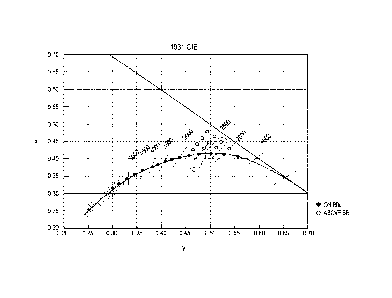
[00104] FIG. 7A provides a portion of a 1931 CIE diagram illustrating the
relationship of various solid state lighting sources to the BBL. Each of the
solid
state lighting devices are modeled to provide a CRI of at least 65 and include
a
blue LED with a mixture of YAG and red phosphors. In particular, the CRI of
the
solid state lighting devices is in a range of about 65 and 75. The phosphor
mixture was varied between the solid state lighting sources to provide data
points
across a range of CCT values. Additionally, solid state lighting sources for
four of
the OCT values were modeled with increasing Duv values. For example, dashed
line 10 circles three data points having a CCT of about 2250 and Duv values of
0
(black circle on the BBL), .005 (white circle above the BBL), and .010 (white
circle
further above the BBL), respectively. A Duv value of .005 corresponds to about
a
5-step MacAdam ellipse above the BBL, and a Duv value of .010 corresponds to
about a 10-step MacAdam ellipse above the BBL. FIG. 7B is a plot comparing
CS values by CCT for each of the data points of FIG. 7A. For CCT values less
than about 2600, the data points on the BBL have CS values that compare
favorably to HPS light sources. Additionally, the CS values are further
decreased
for data points with increased Duv values. For example, dashed line 12 circles
the same three data points as dashed line 10 of FIG. 7A. For OCT values of
about 2250, the CS value progressively decreases (corresponding to reduced
melatonin suppression) as the Duv increases for each data point. Accordingly,
a
solid state lighting device may be configured with Duv values outside of
CA 03101735 2020-11-26
WO 2019/231711
PCT/US2019/032776
24
conventional tolerances to provide a replacement for HPS light sources that
includes a similar CCT, a similar or lower CS value, and a higher CRI.
[00105] FIG. 7C is a table listing the various characteristics for each of the
data
points plotted in FIG. 7A and FIG. 7B. In the table, rows with data points on
the
BBL (Duv of 0) are shaded. The unshaded rows below each shaded row
represent data points with the same CCT and increasing Duv values. Each of the
solid state lighting devices have CRI values in a range of 65 and 75. In
addition
to CS and CLA, other lighting characteristics in the table include luminaire
efficiency rating (LER), CRI, fidelity index (Rf), relative-gamut index (Rg),
R9
prime (R9'), luminous flux (Lx), gamut area index (Qg), lumens per watt (LPW),
and Amelv (a value that is proportional to melanopic lux). (R9' is the same as
R9
for values less than 100 (as shown in FIG. 7C), but is capable of increasing
above 100 for an "oversaturated" condition.) Notably, for each group of CCT
values (e.g. 2000, 2250, 2500, and 2750), the CS and CLA values decrease with
each increase in Duv and the LER and the LPW values increase.
[00106] Accordingly, in some embodiments, a solid state lighting device
comprises a first electrically activated solid state emitter, a first
lumiphoric
material arranged to receive at least a portion of emissions of the first
electrically
activated solid state emitter and responsively generate first lumiphor
emissions,
and at least one other light emitter including at least one of the following
items (a)
or (b): (a) a second electrically activated solid state emitter, or (b) a
second
lumiphoric material arranged to receive at least a portion of emissions of the
first
electrically activated solid state emitter and responsively generate second
lumiphor emissions. Aggregated emissions of the solid state lighting device
include at least a portion of the emissions of each of the first electrically
activated
solid state emitter, the first lumiphoric material, and the at least one other
light
emitter and have a circadian stimulus (CS) value of less than 0.17, and have a
Duv of at least 0.005. In some embodiments, the aggregated emissions have a
CCT of about 2000K (or in a range of 1950K to 2050K), and a CS value of less
than 0.125 ( or in a range from 0.125 to 0.110). In other embodiments, a solid
state lighting device comprises a CCT of about 2250K (or in a range of 2200K
to
2300K), and a CS value of less than 0.145 ( or in a range from 0.145 to 0.12).
In
other embodiments, a solid state lighting device comprises a CCT of about
2550K (or in a range of 2450K to 2550K), and a CS value of less than 0.17 ( or
in
a range from 0.17 to 0.13). As previously described and shown in FIG. 7C , the
CA 03101735 2020-11-26
WO 2019/231711
PCT/US2019/032776
solid state lighting devices having the CCT and CS values described above
comprise a CRI that is at least 65; or in a range of 65 to 75.
[00107] As also shown in FIG. 7C, in some embodiments, a solid state lighting
device comprises a CCT of about 2000K (or in a range of 1950K to 2050K), and
5 an LER value of at least 325 ( or in a range from 325 to 330). In other
embodiments, a solid state lighting device comprises a CCT of about 2250K (or
in a range of 2200K to 2300K), and an LER value of at least 335 ( or in a
range
from 335 to 355). In other embodiments, a solid state lighting device
comprises a
OCT of about 2550K (or in a range of 2450K to 2550K), and an LER value of at
10 least 340 ( or in a range from 340 to 370). As previously described and
shown in
FIG. 70 , the solid state lighting devices having the CCT and LER values
described above comprise a CRI that is at least 65; or in a range of 65 to 75.
[00108] Additionally, multiple data points have LPW values that meet the
technical requirements for efficiency of indoor and outdoor luminaires to
qualify
15 for the DesignLights Consortium (DCL) Premium classification, version
4.3 as of
March 26, 2018. For example, the DLO Premium requirement (version 4.3) for
minimum efficiency of "Outdoor ¨ High Output" luminaires is 120 LPW; and the
DLC Premium requirement (version 4.3) for minimum efficiency of "Outdoor ¨ Mid
Output" luminaires is 115 LPW.
20 [00109] Accordingly, in some embodiments, a solid state lighting device
comprises at least one electrically activated solid state emitter configured
to
generate emissions having a peak wavelength in a blue range, such as 430 nm
to 480 nm; a first lumiphoric material arranged to receive at least a portion
of the
emissions of the at least one electrically activated solid state emitter and
25 responsively generate first lumiphor emissions having a peak wavelength
in a
green/yellow range, such as 540 nm to 570 nm; and a second lumiphoric material
arranged to receive at least a portion of the emissions of the at least one
electrically activated solid state emitter and responsively generate second
lumiphor emissions having a peak wavelength in a red range, such as 605 nm to
650 nm. Aggregated emissions of the solid state lighting device include at
least a
portion of emissions of each of the electrically activated solid state
emitter, the
first lumiphor emissions, and the second lumiphor emissions. In some
embodiments, the aggregated emissions have a OCT in a range of from 1800 K
to 2600 K, and have a Duv of at least 0.005. In further embodiments, the
aggregated emissions have a CCT in a range of about 1800 K to 2300 K; and in
CA 03101735 2020-11-26
WO 2019/231711
PCT/US2019/032776
26
still further embodiments, the aggregated emissions have a CCT in a range of
about 2150 K to 2250 K. In some embodiments, the aggregated emissions have
a Duv in a range from 0.005 to 0.020; in further embodiments, the aggregated
emissions have a Duv in a range from 0.005 to 0.015; and in still further
embodiments, the aggregated emissions have a Duv in a range from 0.005 to
0.010. In some embodiments, the aggregated emissions have a CRI of at least
65. In further embodiments, the aggregated emissions have a CRI of at least
70.
In further embodiments, the aggregated emissions have a CRI in a range of 65
to
85, or in a range of 65 to 80, or in a range of 65 to 85, or in a range of 70
to 90, or
in a range of 70 to 80.
[00110] In some embodiments, the aggregated emissions may include
additional solid state emitters or additional lumiphoric materials. For
example, in
some aspects, solid state lighting device comprises a first electrically
activated
solid state emitter; a first lumiphoric material arranged to receive at least
a portion
of emissions of the first electrically activated solid state emitter and
responsively
generate first lumiphor emissions; a second electrically activated solid state
emitter; and a second lumiphoric material arranged to receive at least a
portion of
emissions of the second electrically activated solid state emitter and
responsively
generate second lumiphor emissions, wherein the second lumiphor emissions
have a peak wavelength that differs from a peak wavelength of the first
lumiphor
emissions by at least 25 nm. Aggregated emissions of the solid state lighting
device include at least a portion of the emissions of each of the first
electrically
activated solid state emitter, the second electrically activated solid state
emitter,
the first lumiphor emissions, and the second lumiphor emissions. In some
embodiments, the aggregated emissions have a correlated color temperature
(CCT) in a range of from 1800 Kelvin (K) to 2600 K, and have a Duv of at least
0.005. In some embodiments, the second lumiphor emissions have a peak
wavelength that differs from the peak wavelength of the first lumiphor
emissions
by at least 35 nm, or by at least 55 nm, or by at least 75 nm, or in a range
of
about 35 nm to about 105 nm. In some embodiments, the first electrically
activated solid state emitter is configured to generate emissions having a
peak
wavelength in a range from 430 nm to 480 nm and the first lumiphor emissions
have a peak wavelength in a range from 540 nm to 570 nm; and the second
electrically activated solid state emitter is configured to generate emissions
having a peak wavelength in a range from 430 nm to 480 nm and the second
CA 03101735 2020-11-26
WO 2019/231711
PCT/US2019/032776
27
lumiphor emissions have a peak wavelength in a range from 605 nm to 650 nm.
In some embodiments, the aggregated emissions have a CRI of at least 65. In
further embodiments, the aggregated emissions have a CRI of at least 70. In
further embodiments, the aggregated emissions have a CRI in a range of 65 to
85, or in a range of 65 to 80, or in a range of 65 to 85, or in a range of 70
to 90, or
in a range of 70 to 80. The aggregated emissions may have additional CCT and
Duv values as described in previous embodiments.
[00111] In some embodiments, a solid state lighting device may comprise an
electrically activated first solid state emitter configured to generate
emissions
having a peak wavelength in a range from 430 nm to 480 nm; an electrically
activated second solid state emitter configured to generate emissions having a
peak wavelength in a range from 605 nm to 650 nm; and a first lumiphoric
material arranged to receive at least a portion of the emissions from at least
one
of the first solid state emitter and the second solid state emitter and
responsively
generate first lumiphor emissions having a peak wavelength in a range from 540
nm to 570 nm. The aggregated emissions from the first and second solid state
emitters and the first and second lumiphor emissions may have a CCT in a range
of from 1800 K to 2600 K and may have a Duv of at least 0.005. Optionally, the
solid state lighting device may further include a second lumiphoric material
arranged to receive at least a portion of the emissions from at least one of
the
first solid state emitter and the second solid state emitter and responsively
generate second lumiphor emissions having a peak wavelength in a range from
605 nm to 650 nm. In further embodiments, the peak wavelength of the second
solid state emitter is different from the peak wavelength of the second
lumiphoric
material within the range from 605 nm to 650 nm.
[00112] In some embodiments, at least one of the first lumiphoric material and
the second lumiphoric material of previous embodiments may include a plurality
of lumiphoric materials. For example, the first lumiphoric material may
comprise
two different lumiphoric materials configured to generate emissions having two
different peak wavelengths within a range from 540 nm to 570 nm. In a similar
manner, the second lumiphoric material may comprise two different lumiphoric
materials configured to generate emissions having two different peak
wavelengths within a range from 605 nm to 650 nm.
[00113] In some embodiments, the first and second lumiphoric materials are
dispersed together in a common binder, such as silicone. In other embodiments,
CA 03101735 2020-11-26
WO 2019/231711
PCT/US2019/032776
28
the first and second lumiphoric materials are arranged in discrete layers. For
example, the second lumiphoric material configured to generate second lumiphor
emissions having a peak wavelength in a range from 605 nm to 650 nm may be
arranged between the first solid state emitter and the first lumiphoric
material
configured to generate first lumiphor emissions having a peak wavelength in a
range from 540 nm to 570 nm. In that regard, for embodiments where the first
lumiphor emissions include wavelengths within the excitation spectrum of the
second lumiphoric material, the amount of first lumiphor emissions received by
the second lumiphoric material may be reduced, thereby improving efficiency.
[00114] Having described desirable combinations of solid state emitters and
lumiphoric materials, solid state lighting devices that may incorporate such
emitters and lumiphoric materials will now be described. In some embodiments,
the first lumiphoric material and the second lumiphoric material are spatially
separated from one another. In some embodiments, the first lumiphoric material
and the second lumiphoric material are spatially separated from the at least
one
solid state emitter.
[00115] In certain embodiments, one or more solid state emitters and
lumiphoric materials as previously described may be provided in a single-chip
or
multi-chip LED package as described below for FIGS. 8-15.
[00116] FIG. 8 illustrates a LED package 100 including a single LED chip 101
mounted on a reflective cup 102 using solder or a conductive epoxy, such that
ohmic contacts for a cathode (or an anode) of the LED chip 101 are
electrically
coupled to the bottom of the reflective cup 102. The reflective cup 102 is
either
coupled to or integrally formed with a first lead 103 of the LED package 100.
One
or more bond wires 104 connect the ohmic contacts for the anode (or cathode)
of
the LED chip 101 to a second lead 105. The reflective cup 102 may be filled
with
an encapsulant material 106 that encapsulates the LED chip 101. The
encapsulant material 106 may be clear or contain one or more wavelength
conversion materials, such as phosphors or other lumiphoric materials. The
entire assembly is encapsulated in a clear protective resin 107, which may be
molded in the shape of a lens to control light emitted from the LED chip 101
and
any lumiphoric material(s) contained in the reflective cup 102.
[00117] An alternative LED package 110 is illustrated in FIG. 9 wherein a LED
chip 111 is mounted on a substrate 114. Ohmic contacts for an anode (or
cathode) of the LED chip 111 are directly mounted to first contact pads 115 on
a
CA 03101735 2020-11-26
WO 2019/231711
PCT/US2019/032776
29
surface of the substrate 114. The ohmic contacts for the cathode (or anode) of
the LED chip 111 are connected to second contact pads 116, which are also on
the surface of the substrate 114, using bond wires 117. The LED chip 111
resides in a cavity of a reflector structure 118, which is formed from a
reflective
material and functions to reflect light emitted from the LED chip 111 through
the
opening formed by the reflector structure 118. The cavity formed by the
reflector
structure 118 may be filled with an encapsulant material 112 that encapsulates
the LED chip 111. The encapsulant material 112 may be clear or contain at
least
one wavelength conversion material, such as one or more phosphors or other
lumiphoric materials.
[00118] FIGS. 10A-13B illustrate exemplary portions of solid state lighting
devices in different configurations incorporating electrically activated solid
state
light emitters and lumiphoric materials arranged over package mounts (or other
substrates) and optionally overlaid with lenses, wherein such devices may be
used alone or in groups according to certain embodiments described herein. It
is
to be appreciated that various structures employed within complete lighting
devices (e.g., package leads, leadframes, contacts, wirebonds, bond
structures,
heat transfer elements, diffusers, additional reflecting surfaces, power
supplies,
and the like) have been omitted for clarity of illustration, but one skilled
in the art
would appreciate that known structures could be incorporated in operative
lighting devices including the illustrative portions provided in FIGS. 16A-
19B.
[00119] FIG. 10A illustrates a solid state light emitting device 120 including
at
least one solid state emitter (e.g., LED) chip 123 (which may include LED
epitaxial layers and a support) arranged over an upper surface 122 of a
package
mount (or other substrate such as a printed circuit board) 121, with a top
surface
124 of the solid state emitter chip 123 being covered with at least one
lumiphoric
material 126 (e.g., a mixture or dispersion of different lumiphoric materials
as
disclosed herein). The package mount 121 may include metalized regions and/or
vias (not shown) for conduction of electrical signals to the solid state
emitter chip
123. Side surfaces 125 of the solid state emitter chip 123 may be exposed, or
in
certain embodiments may be coated with one or more materials or an
encapsulant.
[00120] FIG. 10B illustrates a solid state light emitting device 120A
including
the device 120 of FIG. 10A following the addition of a lens 129 having a
curved
(e.g., substantially hemispherical) shape. The lens 129 may be formed by any
CA 03101735 2020-11-26
WO 2019/231711
PCT/US2019/032776
suitable method, including but not limited to molding using silicone material.
In
certain embodiments, the lens 129 may have a width or lateral extent that is
substantially equal to a width or lateral extent of the package mount 121, and
a
peripheral portion 129A of the lens 129 may have a substantially uniform
5 thickness. In other embodiments, the lens 129 may have a width or lateral
extent
that is less than the width or lateral extent of the package mount 121.
[00121] FIG. 11A illustrates a solid state light emitting device 130 including
a
solid state emitter (e.g., LED) chip 133 (which may include LED epitaxial
layers
and a support) arranged over an upper surface 132 of a package mount (or other
10 substrate such as a printed circuit board) 131, with a top surface 134
and side
surfaces 135 of the solid state emitter chip 133, as well as at least a
portion of the
upper surface 132 of the package mount 131, being covered with a wavelength
conversion (e.g., lumiphoric) material 136. In certain embodiments, the solid
state emitter chip 133 may be mounted to the package mount 131, and thereafter
15 the solid state emitter chip 133 and the upper surface 132 of the
package mount
131 may be coated with the lumiphoric material 136. Coating may be performed
according to any suitable process disclosed herein, such as spray coating,
dipping, or the like. The lumiphoric material 136 may be arranged in a
conformal
layer that follows the shape and outline of multiple surfaces of the solid
state
20 emitter chip 133. Electrical connections to the solid state emitter chip
133 may
be made either before or after coating steps.
[00122] FIG. 11B illustrates a solid state light emitting device 130A
including
the device 130 of FIG. 11A following the addition of a lens 139 having a
substantially rectangular cross-sectional curved (e.g., substantially
25 hemispherical) shape. The lens 139 may be formed by any suitable method,
including but not limited to molding using silicone material. In certain
embodiments, the lens 139 may have a width or lateral extent that is
substantially
equal to a width or lateral extent of the package mount 131. In other
embodiments, the lens 139 may have a width or lateral extent that is less than
30 the width or lateral extent of the package mount 131.
[00123] FIG. 12A illustrates a solid state light emitting device 140 including
a
solid state emitter (e.g., LED) chip 143 (which may include LED epitaxial
layers
and a support) arranged over an upper surface 142 of a package mount (or other
substrate such as a printed circuit board) 141, with a top surface 144 of the
solid
state emitter chip 143 being covered with first through third lumiphoric
material
CA 03101735 2020-11-26
WO 2019/231711
PCT/US2019/032776
31
layers 146, 147, 148. In some embodiments, the solid state emitter chip 143 is
covered with the first and second lumiphoric material layers 146, 147 and the
third lumiphoric material layer 148 is omitted. The package mount 141 may
include metalized regions and/or vias (not shown) for conduction of electrical
signals to the solid state emitter chip 143. Side surfaces 145 of the solid
state
emitter chip 143 may be exposed or otherwise coated with lumiphoric material.
In certain embodiments, the solid state emitter chip 143 may be coated with
the
first through third lumiphoric material layers 146, 147, 148, and thereafter
the pre-
coated solid state emitter chip 143 may be mounted to the package mount 141
followed by establishment of suitable electrically conductive connection(s) to
the
solid state emitter chip 143. Coating may be performed according to any
suitable
process disclosed herein, such as spray coating.
[00124] FIG. 12B illustrates a solid state light emitting device 140A
including
the device 140 of FIG. 12A following the addition of a lens 149 having a
curved
(e.g., substantially hemispherical) shape. The lens 149 may be formed by any
suitable method, including but not limited to molding using silicone material.
In
certain embodiments, the lens 149 may have a width or lateral extent that is
substantially equal to a width or lateral extent of the package mount 141, and
a
peripheral portion 149A of the lens 149 may have a substantially uniform
thickness. In other embodiments, the lens 149 may have a width or lateral
extent
that is less than the width or lateral extent of the package mount 141.
[00125] FIG. 13A illustrates a solid state light emitting device 150 including
a
solid state emitter (e.g., LED) chip 153 (which may include LED epitaxial
layers
and a support) arranged over an upper surface 152 of a package mount (or other
substrate such as a printed circuit board) 151, with a top surface 154 and
side
surfaces 155 of the solid state emitter chip 153, as well as an upper surface
152
of the package mount 151, being covered with first through third lumiphoric
material layers 156, 157, 158. In some embodiments, the solid state emitter
chip
153 is covered with the first and second lumiphoric material layers 156, 157
and
the third lumiphoric material layer 158 is omitted. In certain embodiments,
the
solid state emitter chip 153 may be mounted to the package mount 151, and
thereafter the LED chip 153 and the upper surface 152 of the package mount 151
may be coated with the lumiphoric material layers 156, 157, 158. Coating may
be performed according to any suitable process disclosed herein, such as spray
coating. The lumiphoric material layers 156, 157, 158 may be arranged in
CA 03101735 2020-11-26
WO 2019/231711
PCT/US2019/032776
32
conformal layers that follow the shape and outline of multiple surfaces of the
solid
state emitter chip 153. Electrical connections to the solid state emitter chip
153
may be made either before or after coating steps.
[00126] FIG. 13B illustrates a solid state light emitting device 150A
including
the device 150 of FIG. 13A following the addition of a lens 159 having a
substantially rectangular cross-sectional curved (e.g., substantially
hemispherical) shape. The lens 159 may be formed by any suitable method,
including but not limited to molding using silicone material. In certain
embodiments, the lens 159 may have a width or lateral extent that is
substantially
equal to a width or lateral extent of the package mount 151. In other
embodiments, the lens 159 may have a width or lateral extent that is less than
the width or lateral extent of the package mount 151.
[00127] Although specific lens shapes are illustrated in FIGS. 10B, 1 1B, 12B,
and 13B, it is to be appreciated that lenses according to any suitable shapes
may
be applied to any of the lighting devices illustrated in FIGS. 10A-13B. For
example, symmetric, non-symmetric, polygonal, truncated hemispherical,
faceted, textured, and/or trench-defining lenses may be used.
[00128] FIG. 14 is a side cross-sectional view of at least a portion of a
solid
state light emitting device 160 including multiple solid state emitter (e.g.,
LED)
chips 165 arranged over a submount 161 in a flip-chip configuration, with both
anode and cathode connections on the bottom of the chips 165. The solid state
emitter chips 165 may (optionally) include angled or beveled upper edges with
a
non-rectangular (e.g., polygonal) cross-section, with such shape serving to
enhance light extraction. The solid state emitter chips 165 are coated or
otherwise covered with one or more lumiphoric materials 166 (e.g., in one or
more conformal layers) and arranged under a hemispherical optical element
(e.g., lens) 169, with the conformal layer(s) 166 following the shape and
contour
of multiple surfaces of the solid state emitter chips 165 (preferably with
substantially constant thickness). Such coating may be performed using any
coating technique disclosed herein or otherwise known in the art. As shown in
FIG. 14, the conformal layer(s) 166 may extend over, between and laterally
beyond the solid state emitter chips 165 (such as over a reflective material
disposed between or adjacent to the solid state emitter chips 165). The
optical
element 169 may be separated from the solid state emitter chips 165 via a gap
or
an intervening material 168, which may include an encapsulant or a fluid
medium
CA 03101735 2020-11-26
WO 2019/231711
PCT/US2019/032776
33
such as liquid or gel (e.g., mineral oil, perfluorinated polyether (PFPE)
liquid, or
other fluorinated or halogenated liquid or gel). The intervening material 168
may
also include an index matching medium characterized by a refractive index that
provides for reduced or minimal reflection or internal refraction of light
emissions.
In certain embodiments, elements 168, 169 may embody a single element, such
as molded silicone. In certain embodiments, a thickness of each conformal
layer
166 may be less than half the spacing between adjacent solid state emitter
chips
165. In certain embodiments, spacing between the solid state emitter chips 165
may be on the order of 10 to 75 micrometers, although larger spacing (up to
150
or even 500 micrometers) may also be used. In certain embodiments, the optical
element 169 may include one or more functional materials, such as lumiphoric
material, filtering material, and/or scattering material, which may be doped,
coated, or otherwise provided in or on the optical element 169. Still
referring to
FIG. 14, the submount 161 (e.g., alumina, aluminum nitride, high temperature
polymers, etc.) is covered with a pattern of metal (e.g., traces) 163 that may
be
used to interconnect the solid state emitter chips 165 and provide connection
to a
power supply (not shown). The metal pattern 163 includes connection pads 162
with an insulating material 164 therebetween.
[00129] FIG. 15 illustrates a solid state emitter package 180 including
multiple
solid state emitter (e.g., LED) chips 185 coupled to electrical traces or
metal
patterns 182 via wirebonds 186 and arranged under a hemispherical optical
element (e.g., lens) 189. In certain embodiments, one or more solid state
emitter
chips 185 are coated with one or more lumiphoric materials. As shown, twelve
solid state emitter chips 185 are provided in contact with the electrical
traces or
metal patterns 182 arranged over a submount 181, and cathodes of the solid
state emitter chips 185 are connected by the wirebonds 186 to the electrical
traces or metal patterns 182. In certain embodiments, the optical element 189
may include one or more functional materials, such as lumiphoric material,
notch
filtering material, and/or scattering material, which may be doped, coated, or
otherwise provided in or on the optical element 189. The solid state emitter
chips
185 may be selected from various light color bins to provide a combined light
output with appropriate color characteristics for a desired application. The
unfiltered efficiency of the solid state emitter package 180 with a warm white
color may be on the order of 100 lumens per watt (lm/VV), prior to any
filtering
from the optical element 189; however, if the solid state emitter package 180
is
CA 03101735 2020-11-26
WO 2019/231711
PCT/US2019/032776
34
binned for a cool white color, then an efficiency on the order of about 150
Im/W
can be achieved (i.e., prior to any filtering).
[00130] Embodiments disclosed herein may be suited for various types of
lighting fixtures where melatonin suppression characteristics (i.e., low
melatonin
suppression conditions) that ameliorate or reduce symptoms of circadian rhythm
disorders are desired. The various types of lighting fixtures include both
indoor
and outdoor lighting fixtures. An indoor lighting fixture with melatonin
suppression characteristics described herein may be useful in various
applications, such as night time lighting for hospital rooms where circadian
rhythms of patients may not be disrupted while maintaining good visibility for
doctors and nurses. Other indoor applications may include night time lighting
for
nurseries and other household bedrooms as well as agriculture and livestock
applications. An indoor lighting device may include at least one of an area
light, a
downlight, a high-bay or low-bay lighting fixture, a suspended lighting
fixture, a
troffer, a wall-mounted or ceiling mounted fixture, track lighting, a table or
floor
lamp, and a light bulb. An outdoor lighting fixture with melatonin suppression
characteristics described herein may be useful in various applications,
including
at least one of an area light, a street or roadway light fixture, a canopy
light
fixture, a soffit light fixture, a parking garage lighting fixture, flood
lighting, and a
wall-mounted or ceiling mounted outdoor fixture. In that regard, circadian
rhythms may not be disrupted and light pollution may be reduced.
[00131] FIGS. 16A-16D illustrate a lighting device according to one
embodiment of the disclosure, embodied in a substantially cylindrical
downlight
200 intended for in-ceiling mounting and including multiple LEDs as part of a
LED
module 206. FIG. 16A is a cross-sectional view of the downlight 200 taken
along
the line A-A in FIG. 16B. The downlight 200 includes a generally cylindrical
base
housing 201 and a heatsink housing 205 that in combination form a body
structure. Mounting elements 214 such as rotatable spring tabs are arranged
along an upper surface 215 of the base housing 201. A cable 218 extends
between the base housing 201 and an Edison (screw-type) male connector
forming a threaded lateral contact 212 and a foot contact 211. The base
housing
201 defines an interior volume 202 containing printed circuit boards 203, 204
that
include operative elements such a power converter, a controller module (e.g.,
including at least one processor and a memory), one or more transceivers
(e.g.,
wireless transceivers), LED driver modules, sensor modules, detectors, voice
CA 03101735 2020-11-26
WO 2019/231711
PCT/US2019/032776
recognition circuitry, and the like. The heatsink housing 205 defines an inner
cavity 209 that includes a reflective surface 208 and is further bounded by a
light
transmissive optical element such as a lens and/or a diffuser 210. A trim
bezel
213 is arranged proximate to an open end of the heatsink housing 205. The
5 downlight 200 may include any suitable features disclosed herein, and is
preferably arranged to execute any one or more functions and/or method steps
described herein.
[00132] FIGS. 17A-17B illustrate a light bulb 240 including multiple LEDs 247
arranged in a two-dimensional array within a cavity bounded by a light
10 transmissive globe or lens 250 according to one embodiment of the
disclosure.
Each LED 247 may have associated therewith multiple lumiphoric materials. The
LEDs 247 are arranged on a single substantially planar emitter support surface
246, which may or may not be elevated by a pedestal 254. In other
embodiments, the LEDs 247 may be arranged in strips within an interior volume
15 of the lens 250 to emulate the appearance of an incandescent filament.
The light
bulb 240 includes a body structure 241 having an associated external heatsink
245. An Edison (screw-type) connector including a threaded lateral contact 252
and a foot contact 251 extend from one end of the body structure 241 opposing
the lens 250. The body structure 241 defines an interior volume containing at
20 least one printed circuit board (not shown) that includes operative
elements such
as a power converter, a controller module (e.g., including at least one
processor
and a memory), one or more transceivers (e.g., wireless transceivers), LED
driver
modules, sensor modules, detectors, voice recognition circuitry, and the like.
The
light bulb 240 may include any suitable features disclosed herein.
25 [00133] FIGS. 18A-18B illustrate a troffer-type (in-ceiling linear)
light fixture 300
arranged to incorporate multiple solid state emitters (e.g., LEDs) 326 as
disclosed
herein. In certain embodiments, one or more lumiphoric materials may be
associated with one or more solid state emitters 326. Optionally, the light
fixture
300 may include one or more notch filtering materials, such as may be
30 .. associated with the solid state emitters 326, which may be applied to or
included
in a linear reflector (e.g., by doping, impregnation, coating, etc.), or may
be
applied to or integrated with one or more light transmissive lens plates 315,
316
to cause the light emitted from the light fixture 300 to exhibit a spectral
notch.
The light fixture 300 includes a pan 301, a heatsink 302, a reflector 308, and
end
35 caps 310, 311. The end cap 310 is larger than the end cap 311 and is
shaped to
CA 03101735 2020-11-26
WO 2019/231711
PCT/US2019/032776
36
act as a circuit box to house electronics (e.g., rectifiers, regulators,
timing
circuitry, etc.) used to drive and control the light source. The reflector 308
may
include a diffusively reflective or specularly reflective surface 318.
Although a
reflector may take various shapes, in the illustrated embodiment, the
reflector 308
includes a flat region 324 opposite the heatsink 302. In alternative
embodiments,
the reflector 308 could be parabolic in shape, or include two or more
parabolic
regions. The light fixture 300 also includes a diffuser lens assembly
including the
lens plates 315, 316, disposed adjacent to sides of the heatsink 302. As
illustrated, the one or more solid state emitters 326 are arranged facing the
reflector 308 in a manner such that a majority of LED emissions interact with
the
reflector 308 before exiting the light fixture 300 via the lens plates 315,
316. In
alternative embodiments, the one or more solid state emitters 326 are arranged
facing the lens plates 315, 316 such that a smaller portion of LED emissions
interact with the reflector 308 before exiting the light fixture 300. In such
embodiments, the lens plates 315, 316 may be replaced with a single continuous
lens plate that covers the reflector 308.
[00134] FIGS. 19A-19B illustrate a high bay/low bay type solid state lighting
fixture 330 including a frame 332 over which a heatsink 334 and an electronics
housing 336 are mounted. An LED array 338 is mounted on a bottom side of the
frame 332 and may be covered by a lens 340. As illustrated, a portion of the
lens
340 is shown as being removed to expose the LED array 338. A reflector 342
may be provided around the LED array 338 to aid in directing and mixing light
emitted from the LED array 338 for general illumination.
[00135] FIGS. 20A-20E illustrate a first outdoor floodlight (e.g., street or
roadway lamp) lighting fixture 350 that may include solid state light emitters
and
lumiphoric materials according to embodiments described herein. With reference
to FIG. 20A, the lighting fixture 350 is mounted to a utility pole 352 by a
tenon
354. The tenon 354 in this example extends outward from a top portion of the
utility pole 352, and the lighting fixture 350 is attached to the free end of
the tenon
354. The bottom of the utility pole 352 may be mounted to a pole base 356,
which is securely mounted in or on the ground or other surface. As provided
herein, the tenon 354 is defined as the mounting structure to which the
lighting
fixture 350 is directly mounted. The tenon 354 may be an integral extension or
part of the utility pole 352, attached to the utility pole 352, or attached
directly to a
structure other than a pole, such as a building, wall, frame, sign, and the
like.
CA 03101735 2020-11-26
WO 2019/231711
PCT/US2019/032776
37
[00136] Typically, the lighting fixture 350 has a housing 358 in which a light
source 360 and an ambient light sensor 362 are mounted. In normal operation,
the ambient light sensor 362 provides information bearing on ambient light
levels,
and based on these ambient light levels, the light source 360 will turn on and
off.
When ambient light levels fall below a certain level, the light source 360
will turn
on, and when ambient light levels rise above a certain level, the light source
360
will turn off in traditional fashion. While the light source 360 may take
various
configurations, the one illustrated incorporates LEDs and sufficient control
circuitry to drive the LEDs as desired in response to information provided by
the
ambient light sensor 362 as well as any other sensors, such as occupancy,
motion, sound, vibration, temperature, and like sensors, as well as a wired or
wireless controllers. As described further below, an access cover 364 provides
access to the interior of the housing 358. Such access may facilitate
connecting
the light source power as well as securely attaching the lighting fixture 350
to the
tenon 354. In some embodiments, the access cover 364 is hinged at the rear of
the housing 358 and rotates downward to provide access to the interior of the
housing 358. The access cover 364 may use various mechanisms to lock into a
closed position. These mechanisms may range from fasteners, such as screws
and bolts, to snap-fit and magnetic configurations.
[00137] The housing 358 and the access cover 364 may be formed using an
over-molding process that employs various mold compounds, such as thermoset
bulk molding compounds, fiber reinforced thermoplastics, or un-filled
thermoplastics. These mold compounds may be polymer based, but are not
limited thereto, and may include various types of fibers, such as glass
fibers, for
reinforcement. With an over-mold process, the housing 358 and the various
features thereof may be integrally formed as a single structure. Further,
various
features that are provided on or within the housing 358 may be affixed to,
surrounded by, or otherwise formed within the structure. The tenon 354 may be
formed from the same or different materials as the housing 358. In various
embodiments, the tenon 354 may be formed from metals, such as, aluminum and
steel, as well as from composite materials, such as carbon reinforced polymers
and the like.
[00138] FIG. 20B provides a rear isometric view of the lighting fixture 350,
including a view of the housing 358 and the ambient light sensor 362 that is
on an
opposite side of the lighting fixture 350 from the access cover 364. An
opening at
CA 03101735 2020-11-26
WO 2019/231711
PCT/US2019/032776
38
the rear of the lighting fixture 350 is referred to as a tenon cradle 366. The
tenon
cradle 366 receives the tenon 354, and an attachment mechanism, which will be
described further below, is used to securely attach the lighting fixture 350
to the
tenon 354. FIGS. 200, 20D, and 20E, provide side, front, and bottom views,
respectively, of the lighting fixture 350 including the housing 358, the light
source
360, the ambient light sensor 362, the access cover 364, and the tenon cradle
366. As previously described, the light source 360 includes LEDs and
sufficient
control circuitry to drive the LEDs. The light source 360 may further include
one
or more lenses or reflectors configured to direct light in a desired emission
pattern. In some embodiments, the light source 360 includes a waveguide, or a
waveguide optic, configured to receive light from the LEDs and direct it in a
desired emission pattern.
[00139] FIGS. 21A-21B illustrate a second outdoor floodlight (e.g., street or
roadway lamp) lighting fixture 400 that may include solid state light emitters
and
lumiphoric materials as described herein. The lighting fixture 400 includes a
housing 410 including a base portion 411 supported by an elongated pole 401 or
other support. Multiple LEDs modules 431-1, 431-2, 431-3 each including
multiple LEDs 418A, 418B arranged in an array are provided along a lower
surface 420 of the lighting fixture 400 between the pole 401 and an end cap
412.
The LED modules 431-1, 431-2, 431-3 are arranged proximate to an air gap 414
permitting heat to be dissipated to a heat spreader or heat sink 426 (arranged
along an upper surface 413 of the housing 410) and transferred to an ambient
environment. The lighting fixture 400 may include at least one receiver or
sensor
element 440-1, 440-2, which may embody any one or more of a GPS receiver, a
radio frequency receiver, an ambient light sensor, an image sensor, a
temperature sensor, a motion sensor, a sound sensor, a timer, or the like.
[00140] FIGS. 22A-22B illustrate a third outdoor floodlight (e.g., street or
roadway lamp) lighting fixture 450 including a body structure 402 housing an
array of solid state light emitters 404 as disclosed herein. An interface
structure
406 may be used to couple the lighting fixture 450 to a pole 410. Outdoor
light
fixtures such as shown in FIGS. 27A-27B may be mounted to poles, tenons, or
the like. The array of solid state light emitters 404 may be used to
illuminate a
desired environment, such as a roadway, a parking lot, a street, or the like.
[00141] Any of the lighting fixtures described in FIGS. 16A-16D, 17A-17B, 18A-
18B, 19A-198, 20A-20E, 21A-21B, and 22A-22B may be configured to provide
CA 03101735 2020-11-26
WO 2019/231711
PCT/US2019/032776
39
aggregated emissions having a COT in a range of from about 1800 K to about
2600 K. In further embodiments, the aggregated emissions have a COT in a
range of from about 1800 K to about 2300 K, or in a range of from about 2150 K
to 2250 K. In some embodiments, the aggregated emissions have a Duv in a
range from 0.005 to 0.020; in further embodiments, the aggregated emissions
have a Duv in a range from 0.005 to 0.015; and in still further embodiments,
the
aggregated emissions have a Duv in a range from 0.005 to 0.010. In some
embodiments, the aggregated emissions have a CRI of at least 65. In further
embodiments, the aggregated emissions have a CRI of at least 70. In further
embodiments, the aggregated emissions have a CRI in a range of 65 to 85, or in
a range of 65 to 80, or in a range of 70 to 90, or in a range of 70 to 80.
[00142] In some embodiments, any of the lighting fixtures described in FIGS.
16A-16D, 17A-17B, 18A-18B, 19A-19B, 20A-20E, 21A-21B, and 22A-22B have
multiple LEDs, each of which is configured to provide the same aggregated
emissions as previously described. In other embodiments, different LEDs of the
multiple LEDs have different emission characteristics that collectively form
the
aggregated emissions of a particular lighting fixture. For example, a solid
state
lighting device may include a first electrically activated solid state emitter
configured to generate emissions having a peak wavelength in a range from 430
nm to 480 nm, a first lumiphoric material arranged to receive at least a
portion of
the emissions of the first electrically activated solid state emitter and
responsively
generate first lumiphor emissions having a peak wavelength in a range from 540
nm to 570 nm, a second electrically activated solid state emitter configured
to
generate emissions having a peak wavelength in a range from 430 nm to 480
nm, and a second lumiphoric material arranged to receive at least a portion of
the
emissions of the second electrically activated solid state emitter and
responsively
generate second lumiphor emissions having a peak wavelength in a range from
605 nm to 650 nm. Aggregated emissions of the solid state lighting device
thereby include a portion of emissions of the first and second electrically
activated solid state emitters, the first lumiphor emissions, and the second
lumiphor emissions.
[00143] Embodiments as disclosed herein may provide one or more of the
following beneficial technical effects: reducing circadian rhythm disruptions
of
illumination provided by lighting devices while maintaining desirable color
CA 03101735 2020-11-26
WO 2019/231711
PCT/US2019/032776
rendering characteristics; reducing light pollution in the night sky; and
reducing
energy consumption required for light fixtures.
[00144] Those skilled in the art will recognize improvements and modifications
to the preferred embodiments of the present disclosure. All such improvements
5 and modifications are considered within the scope of the concepts
disclosed
herein and the claims that follow.