Note: Descriptions are shown in the official language in which they were submitted.
MULTI-BAND PLANAR ANTENNA
BACKGROUND
[0001] Dipole antennas are commonly used for wireless communications. A
dipole antenna
typically includes two identical conductive elements to which a driving
current from a
transmitter is applied, or from which a received wireless signal is applied to
a receiver. A dipole
antenna most commonly includes two conductors of equal length oriented end-to-
end with a
feedline connected between them. A half-wave dipole includes two quarter-
wavelength
conductors placed end to end for a total length (L) of approximately L=V2,
where X, is the
wavelength corresponding to the intended frequency (f) of operation. A folded
dipole antenna
consists of a half-wave dipole with an additional wire connecting its two
ends. The far-field
emission pattern of the folded dipole antenna is nearly identical to the half-
wavelength dipole,
but typically has an increased impedance and a wider bandwidth. Half-
wavelength folded
dipoles are used for various applications including, for example, for
Frequency Modulated (FM)
radio antennas.
SUMMARY
[0002] According to a broad aspect, there is provided an antenna,
comprising: a first folded
dipole forming a first loop and comprising a first central non-conductive
region within an interior
of the first loop; a second folded dipole forming a second loop and comprising
a second central
non-conductive region within an interior of the second loop, wherein the
second folded dipole is
connected in parallel to the first folded dipole; a first pair of tuning stubs
connected to opposing
sides of the first folded dipole within the first central non-conductive
region of the first loop and
extending into the first central non-conductive region within the interior of
the first loop; and a
second pair of tuning stubs connected to opposing sides of the second folded
dipole within the
- 1 -
Date Recue/Date Received 2022-03-30
second central non-conductive region of the second loop and extending into the
second central
non-conductive region within the interior of the second loop. According to
another broad aspect,
there is provided an antenna structure, comprising: a dielectric; a conductor
layout formed on the
dielectric, wherein the conductor layout comprises: a first folded dipole
forming a first loop and
comprising a first central non-conductive region within an interior of the
first loop, a second
folded dipole forming a second loop and comprising a second central non-
conductive region
within an interior of the second loop, wherein the second folded dipole is
coupled in parallel to
the first folded dipole, a first pair of tuning stubs connected to opposing
sides of the first folded
dipole within the first central non-conductive region of the first loop and
extending into the first
central non-conductive region within the interior of the first loop, and a
second pair of tuning
stubs connected to opposing sides of the second folded dipole within the
second central non-
conductive region of the second loop and extending into the second central non-
conductive
region within the interior of the second loop; and a feed line conductor
formed on the dielectric
and coupled to a feed section of the first and second folded dipoles.
BRIEF DESCRIPTION OF THE DRAWINGS
[0003] FIG. 1 depicts a three-dimensional view of a folded dipole antenna
structure
according to an exemplary implementation;
[0004] FIG. 2A depicts a two-dimensional top view of the first side of the
antenna structure
depicted in FIG. 1;
[0005] FIG. 2B depicts a two-dimensional "see-through" view of the second
side of the
antenna structure depicted in FIG. 1;
[0006] FIG. 3 depicts further details of the antenna conductor layout on
the first side of the
planar dielectric of FIG. 1 according to one exemplary implementation;
- 2 -
Date Recue/Date Received 2022-03-30
[0007]
FIG. 4A illustrates an expanded view of a first radiating section of a first
folded
dipole of the conductor layout of FIG. 3;
[0008]
FIG. 4B illustrates an expanded view of a second radiating section of a second
folded
dipole of the conductor layout of FIG. 3;
[0009]
FIG. 5 illustrates an expanded view of the feed section of the conductor
layout of
FIG. 3;
[0010]
FIG. 6 depicts further details of the conductor layout on the second side of
the planar
dielectric of FIG. 1 according to an exemplary implementation;
[0011]
FIG. 7 depicts a plot of Voltage Standing Wave Ratio versus frequency for an
exemplary folded dipole antenna structure corresponding to FIG. 1;
[0012]
FIGs. 8A and 8B illustrate three-dimensional radiation patterns associated
with the
folded dipole antenna structure of FIG. 1 at a frequency of 750 Megahertz;
[0013]
FIGs. 9A and 9B illustrate three-dimensional radiation patterns associated
with the
folded dipole antenna structure of FIG. 1 at a frequency of 1800 Megahertz;
and
[0013a]
FIGs. 10A and 10B illustrate three-dimensional radiation patterns associated
with
the folded dipole antenna structure of FIG. 1 at a frequency of 2150
Megahertz.
DETAILED DESCRIPTION OF EMBODIMENTS
[0014] Variants, examples, and preferred embodiments of the invention are
described
hereinbelow. The following detailed description refers to the accompanying
drawings. The same
reference numbers in different drawings may identify the same or similar
elements. The
Date Recue/Date Received 2022-03-30
following detailed description does not limit the invention.
[0015] A compact folded dipole antenna structure, as described herein,
includes two
parallel connected, folded dipoles that may be formed on a first side of a
planar dielectric,
such as a printed circuit board (PCB), and a feed line and a tunable impedance
matching
element that may be formed on a second, opposite side of the planar
dielectric. The resulting
antenna structure is compact and self-resonant such that the antenna structure
does not need to
be attached to another structure to resonate. Each of the folded dipoles of
the antenna
structure includes, within a non-conductive central region of each folded
dipole, a pair of
tuning stubs that control higher resonant frequencies of the antenna
structure. Various
dimensions associated with the pair of tuning stubs may be tuned to adjust the
higher resonant
frequencies of the antenna structure.
[0016] The antenna structure of the compact folded dipole antenna
further includes a first
tuning element and a second tuning element connected to an antenna feed
section associated
with the first folded dipole and the second folded dipole. The first and
second tuning
elements may be formed on the first side of the planar dielectric and control
lower resonant
frequencies of the antenna structure. Various dimensions associated with the
first and second
tuning elements may be tuned to adjust the lower resonant frequencies of the
antenna
structure.
[0017] The tunable impedance matching element that may be formed on the
second side
of the planar dielectric and extend across a gap between respective portions
of the antenna
feed section associated with the two folded dipoles. Since current is balanced
in the layout of
the antenna structure, no external balun needs to be used with the antenna
structure. The feed
line that may be formed on the second side of the planar dielectric may also
include a
-3-
Date Recue/Date Received 2020-12-09
microstrip feed line that may be formed integrally with the antenna conductor
layout,
eliminating a need for an external coaxial structure.
[0018] The compact folded dipole antenna structure described herein may
resonate at
multiple different frequencies spanning a range from approximately 675
Megahertz (MHz) to
approximately 2500 MHz. The pairs of tuning stubs of the two parallel-
connected folded
dipoles, and the tuning elements connected to the respective antenna feed
sections of the two
folded dipoles, may be tuned to adjust both the lower and higher resonant
frequencies of the
antenna structure.
[0019] The antenna structure described herein may be used in, for
example, a meter such
as a utility meter (e.g., a water meter or power usage meter) to transmit and
receive data. For
example, the antenna structure may be a component of a meter interface unit
within the utility
meter that enables wireless communication to/from the utility meter in
multiple different
bands (e.g., Long-Term Evolution (LTE) bands 4 and 13, 900 MHz Industrial,
Scientific, and
Medical (ISM) band, 2.4 GHz ISM (Bluetooth')). The compact nature of the
antenna
structure, requiring the use of no external components (e.g., no components on
an external
PCB), enables the antenna to be fit within the physical constraints of
existing meter interface
units, or more easily fit within newly designed meter interface units that may
be relatively
small in size.
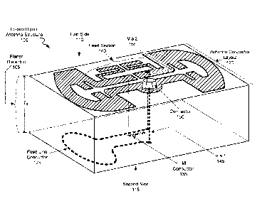
[0020] FIG. 1 depicts a three-dimensional view of a folded dipole
antenna structure 100
according to an exemplary implementation. As shown, the folded dipole antenna
structure
100 includes a planar dielectric 105 having a first side 110, and an opposite,
second side 115.
In the example shown, first side 110 may be a "top" side and the second side
115 may be a
"bottom" side. Planar dielectric 105 may include one or more of various types
of dielectric
-4-
Date Recue/Date Received 2020-12-09
material, such as, for example, fiberglass, glass, plastic, mica, and metal
oxide, and may have
a thickness (Td) ranging from approximately 0.008 inches to about 0.24 inches.
In one
exemplary implementation, planar dielectric 105 may have a thickness LI of
0.032 inches.
The first side 110 of planar dielectric 105 has an antenna conductor layout
120 formed upon
it. The antenna conductor layout 120 forms two parallel-connected folded
dipoles, as
described in further detail below.
[0021] The second side 115 of planar dielectric 105 includes a feed line
conductor 125,
and an impedance matching (IM) conductor 135 formed thereon. Feed line
conductor 125
traces a pattern upon the second side 115 of planar dielectric 105 to connect
a feed connector
150, through a via 1 145, to an antenna feed section 140 (described further
below) of the
antenna conductor layout 120 on the first side 110 of planar dielectric 105.
In an example in
which a transmitter (not shown) transmits signals via the antenna structure
100, the
transmitter signals are received by the center conductor of feed connector
150, conveyed
through via 1 145 to feed line conductor 125, conveyed along a length of the
feed line
conductor 125, and conveyed through a via 2 155 to the feed section 140 of the
folded dipoles
on the first side 110 of planar dielectric 105. In other implementations,
signals may be
conveyed from to feed section 140 via an open or shorted stub line. In an
example in which a
receiver (not shown) receives signals via the antenna structure 100, wireless
signals received
by antenna structure 100 are conveyed, via the feed section 140, through via 2
155, along a
length of the feed line conductor 125, and conveyed through via 1 145 to the
center conductor
of feed connector 150.
[0022] IM conductor 135 includes a conductive trace that is formed at a
position upon the
second side 115 of planar dielectric 105 that is opposite of feed section 140
of conductor
-5-
Date Recue/Date Received 2020-12-09
layout 120 on the first side 105 of planar dielectric 105 such that conductor
135 is
capacitively coupled, across planar dielectric 105 to the feed section 140 of
conductor 120 on
the first side 110 of planar dielectric 105. The second side 115 of planar
dielectric 105 may
optionally have a secondary impedance matching conductor (not shown) formed at
a location
along the length of the feed line conductor 125.
[0023] FIG. 2A depicts a two-dimensional "top" view of the first side
110 of antenna
structure 100. FIG. 2B depicts a two-dimensional "see-through" view of the
second side 115
of antenna structure 100. In the view of FIG. 2B, the material of planar
dielectric 105 is
depicted as transparent such that the underlying conductor layouts on the
underside of planar
dielectric 105 can be clearly seen. Returning to FIG. 2A, a left portion of
the antenna
conductor layout 120 includes a first folded dipole 200, and a right portion
of the antenna
conductor layout 120 includes a second folded dipole 205. As shown, feed
connector 150
includes a common (e.g., ground) connection to the antenna conductor layout
120 via a
connector sleeve 210 of connector 150. Both folded dipoles 200 and 205 are
electrically
connected to the common connection at feed connector 150. The center conductor
215 of
connector 150 acts as the feed conductor and either supplies a transmitter
signal (not shown)
to feed line conductor 125 (FIG. 2B) through via 1 145 (not shown) or supplies
a received
signal from feed line conductor 125 and via 1 145 to a receiver (not shown)
connected to
connector 150. Feed line conductor 125 (FIG. 2B) supplies the transmitter
signal through via
2 155 to feed section 140 of the antenna conductor layout 120. Therefore,
folded dipole 200
and folded dipole 205 are connected in parallel with one another between the
common
connection at connector 150 and the feed connection from center conductor 215
of connector
150 (i.e., through via 2 155 to feed line conductor 125, through via 2 155, to
feed section
-6-
Date Recue/Date Received 2020-12-09
140).
[0024] As shown in FIG. 2A, feed section 140 includes two frequency
tuning elements
220, with the left-most tuning element being associated with folded dipole 1
200, and the
right-most tuning element being associated with folded dipole 2 205. Each of
the frequency
tuning elements 220 may be modified to tune the lower resonance frequencies of
antenna
structure 100. A central region 240-1 of folded dipole 200 and a central
region 240-2 of
folded dipole 205 each includes additional pairs of frequency tuning elements
230. The left-
most pair of tuning elements 230 are associated with folded dipole 1 200, and
the right-most
pair of tuning elements 230 are associated with folded dipole 2 205. Each of
the pairs of
frequency tuning elements 230 may be modified to tune the higher resonance
frequencies of
antenna structure 100.
[0025] As illustrated in FIGs. 2A and 2B, IM conductor 135 includes a
conductive strip
having, for example, a rectangular shape, that extends across a gap between
the left side of
feed section 140 to a right side of feed section 140 to electrically couple
the two sides. In one
implementation, IM conductor 135 may capacitively couple, across the
dielectric material of
planar dielectric 105, the left side of feed section 140 to the right side of
feed section 140. In
another implementation, two conductive vias (not shown) may extend through the
planar
dielectric 105 to connect a first end of IM conductor 135 to a left side of
feed section 140, and
a second end of IM conductor 135 to a right side of feed section 140. The
registration or
location of IM conductor 135, on second side 115, with the two sides of feed
section 140 on
the first side 110 is shown with dotted lines in the center of the conductor
layout 120 in FIG.
2A. Additional details regarding dimensions of the components of an exemplary
implementation of antenna conductor layout 120 are described below with
respect to FIGs. 3,
-7-
Date Recue/Date Received 2020-12-09
4A, 4B, and 5.
[0026] As shown in FIG. 2B, via 1145, which passes through the
dielectric material of
planar dielectric 105, electrically connects to a first end of feed line
conductor 125. The feed
line conductor 125 traces a circuitous pattern upon second side 115 of planar
dielectric 105
that follows a portion of the pattern of antenna conductor layout 120 on the
first side 110. A
first end of feed line conductor 125 connects to center conductor 215 of
connector 150 (FIG.
2A) through via 1 145, and a second end of feed line conductor 125 connects to
feed section
140 of antenna conductor layout 120 through via 2 155. Additional details
regarding
dimensions of the various components formed on second side 115 of planar
dielectric 105 of
an exemplary implementation are described below with respect to FIG. 6.
[0027] FIG. 3 depicts further details of antenna conductor layout 120 on
first side 110 of
the planar dielectric 105 according to one exemplary implementation. As shown,
folded
dipole 1 200 and folded dipole 2 205 of antenna conductor layout 120 may each
have a length
la and a width lb. In one exemplary implementation, length la may be 2.450
inches and
width lb may be 2.400 inches. Further, each of folded dipoles 200 and 205 may
be bisected
with a center line that divides the width lb to create a width lc. In one
implementation, lc =
1/2*lb.
[0028] As further depicted in FIG. 3, antenna conductor layout 120
includes feed section
140, a first radiating section 300-1 (corresponding to the folded portion of
dipole 1 200, a
second radiating section 300-2 (corresponding to the folded portion of dipole
2 205), and a
common section 305. In one exemplary implementation, a length ld of first
radiating section
300-1 and second radiating section 300-2 may be 1.270 inches.
[0029] Feed section 140 may be divided into two sections, each having a
length le and a
-8-
Date Recue/Date Received 2020-12-09
width if and each separated from one another by a gap G1 in the conductor
material. In one
exemplary implementation, the two sections of feed section 140 may have a
length le of
1.170 inches, a width if of 0.315 inches, and a gap G1 of 0.020 inches. The
two sections,
each having a length le, of feed section 140 may be separated from common
section 305 of
antenna conductor layout 120 by a gap G2. In one exemplary implementation, the
gap G2
may be 0.135 inches. Common section 305 may additionally have a width if
similar to width
If of the two sections of feed section 140.
[0030] Folded dipole 200 300-1 includes a feed arm 310-1 that connects
to a non-feed
arm 315-1. Folded dipole 205 includes a feed arm 310-2 that connects to a non-
feed arm 315-
2. Feed arms 310-1 and 310-2 connect, respectively, to each of the two feed
sections 140
having length le. Non-feed arm 315-1 and non-feed arm 315-2 both connect to
common
section 305. Radiating section 300-1 of folded dipole 200 includes a non-
conductive central
region 240-1 formed inside the conductive traces of the folded dipole 200
(e.g., inside feed
arm 310-1 and non-feed arm 315-1). Radiating section 300-2 of folded dipole
205 also
includes a non-conductive central region 240-2 formed inside the conductive
traces of folded
dipole 205 (e.g., inside feed arm 310-2 and non-feed arm 315-2). Central
regions 240-1 and
240-2 may have similar configurations and dimensions, as described further
below with
respect to FIGs. 4A and 4B.
[0031] FIG. 4A illustrates an expanded view of the radiating section 300-
1 of folded
dipole 200. As shown, the central region 240-1 of folded dipole 200 includes a
pair of tuning
stubs 230-1 formed as part of the conductive layout 120 on the upper and lower
side of central
region 240-1. Central region 240-1 has a length 4b and a width 4a. In one
implementation,
length 4b may be 0.525 inches and width 4a may be 0.950 inches. The upper
tuning stub of
-9-
Date Recue/Date Received 2020-12-09
stubs 230-1 may have a length 4d and a width 4c. Similarly, the lower tuning
stub of stubs
230-1 may have a length 4d and a width 4c. In one implementation, length 4d
may be
0.223inches and width 4c may be 0.350 inches. As shown, the portion of the
conductive
layout 120 on the upper side of central region 240-1 may have a width of 4e,
and the portion
of the conductive layout on the lower side of central region 240-1 may also
have a width of
4e. In one implementation, 4e may be 0.725 inches. The portion of the
conductive layout 120
on the left side of central region 240-1 may have a length of 4f In one
implementation, 4f
may be 0.350 inches. Each of tuning stubs 230-1 may be located a distance 4g
from the left-
most edge of central region 240-1, and a distance 4h from the right-most edge
of central
region 240-1 of folded dipole 200. In one implementation, 4g may be 0.252
inches and 4h
may be 0.050 inches.
[0032] FIG. 4B depicts an expanded view of the radiating section 300-2
of folded dipole
205. As shown, the central region 240-2 of folded dipole 205 includes a pair
of tuning stubs
230-2 formed as part of the conductive layout 120 on the upper and lower side
of central
region 240-2. Central region 240-2 has a length 4b and a width 4a. In one
implementation,
length 4b may be 0.525 inches and width 4a may be 0.950 inches. The upper
tuning stub of
stubs 230-2 may have a length 4d and a width 4c. Similarly, the lower tuning
stub of stubs
230-2 may have a length 4d and a width 4c. In one implementation, length 4d
may be 0.223
inches and width 4c may be 0.350 inches. As shown, the portion of the
conductive layout 120
on the upper side of central region 240-2 may have a width of 4e, and the
portion of the
conductive layout on the lower side of central region 240-2 may also have a
width of 4e. In
one implementation, 4e may be 0.725 inches. The portion of the conductive
layout 120 on the
right side of central region 240-2 may have a length of 4f In one
implementation, 4f may be
-10-
Date Recue/Date Received 2020-12-09
0.350 inches. Each of tuning stubs 230-2 may be located a distance 4g from the
right-most
edge of central region 240-2, and a distance 4h from the left-most edge of
central region 240-
2 of folded dipole 205. In one implementation, 4g may be 0.252 inches and 4h
may be 0.050
inches. The various dimensions of tuning stubs 230-1 and 230-2 (e.g., 4c, 4d,
4h, 4g), and
radiating sections 300-1 and 300-2 (e.g., 4a, 4f 4b, 4e) may be modified to
tune the higher
resonance frequencies of antenna structure 100.
[0033] FIG. 5 illustrates an expanded view of feed section 140 of
conductor layout 120.
The frequency tuning elements 220 of feed section 140 include a first
frequency tuning
element 500-1 and a second frequency tuning element 500-2. Frequency tuning
element 500-
1 connects to the left-most portion of feed section 140 at a distance 5a from
feed arm 310-1 of
radiating section 300-1. A conductive trace of frequency tuning element 500-1
has a length
Li and has a width of 5b extending most of the length Li. Another portion of
frequency
tuning element 500-1 has a length 5d length and a width of 5c. Frequency
tuning element
500-2 connects to the right-most portion of feed section 140 at a distance 5a
from feed arm
310-2 of radiating section 300-2. A conductive trace of frequency tuning
element 500-2 has
the length Li and has a width of 5b extending most of the length Li. Another
portion of
frequency tuning element 500-2 has a length 5d and a width of Sc. In one
exemplary
implementation, 5a may be 0.180 inches, 5b may be 0.044 inches, Sc may be
0.145 inches,
and 5d may be 0.840inches. As shown in FIG. 5, the conductive traces of
frequency tuning
elements 500-1 and 500-2 may be formed in a winding or circuitous shape that
enables the
lengths Li to fit within a limited space upon first side 110 of planar
dielectric 105 within
antenna feed section 140, thereby minimizing the use of an area upon or within
planar
dielectric 105. The various dimensions of frequency tuning elements 500-1 and
500-2 may be
-11 -
Date Recue/Date Received 2020-12-09
modified to tune the lower resonance frequencies of antenna structure 100.
[0034] FIG. 6 depicts further details of the second side 115 of the
planar dielectric 105
according to one exemplary implementation. As shown, feed line conductor 125
may include
a conductive microstrip line that traces a path, that roughly corresponds to a
shape of a portion
.. of antenna conductor layout 120 on the first side 110, from a connection
with via 1 145 to a
connection with via 2 155. An optional impedance matching element (not shown),
including
a conductive element having a length and a width, may be formed at a distance
from the
connection to via 1 145 along the conductive strip-line of feed line conductor
125 upon
second side 115. The length, width, and distance of the optional impedance
matching element
along the conductive strip-line of feed line conductor 125 may each be
selected to adjust the
impedance of folded dipole antenna structure 100 for impedance matching.
[0035] As further shown in FIG. 6, IM conductor 135 may include a
conductive element
having a length 6a and a width 6b, formed upon second side 115 such that a
first end (the left
side of element 135) is disposed opposite the left portion of feed section 140
of antenna
conductor layout 120 to enable the first end to capacitively couple to the
left end of feed
section 140 through the dielectric material of planar dielectric 105.
Additionally, IM
conductor 135 may be formed upon second side 115 such that a second end (the
right side of
IM conductor 135) is disposed opposite the right portion of feed section 140
of antenna
conductor layout 120 to enable the second end to capacitively couple to the
right end of feed
section 140 through the dielectric material of planar dielectric 105. IM
conductor 135,
therefore, electrically couples across gap G1 (FIG. 3) between the two
separate sections of
feed section 140 of antenna conductor layout 120. In one exemplary
implementation, length
6a may be 0.400 inches and width 6b may be 0.040 inches. The length 6a of IM
conductor
-12-
Date Recue/Date Received 2020-12-09
135 may be selected so as to tune the impedance of antenna structure 100.
[0036] FIG. 7 depicts a plot 700 of Voltage Standing Wave Ratio (VSWR)
versus
frequency for an exemplary implementation of the folded dipole antenna
structure 100
described herein. The x-axis of the plot 700 includes frequency, ranging from
500 MegaHertz
(MHz) to 2.5 GigaHertz (GHz). The y-axis of the plot 700 includes VSWR,
ranging from
1.00 to 4.00. As is understood in the art, for a transmitter to deliver power
to an antenna, or
receive power from the antenna, the impedance of the transmitter/receiver and
the
transmission line must be well matched to the antenna's impedance. The VSWR
parameter of
an antenna numerically measures how well the antenna is impedance matched to
the
transmitter/receiver. The smaller an antenna's VSWR is, the better the antenna
is matched to
the transmitter/receiver and the transmission line, and the more power is
delivered to/from the
antenna. The minimum VSWR of an antenna is 1.0, at which no power is reflected
from the
antenna. Bandwidth requirements of antennas are typically expressed in terms
of VSWR.
For example, an antenna for a particular application may need to operate from
1.0 GHz to
1.3GHz with a VSWR less than 3Ø
[0037] In the plot 700 of FIG. 7, the plotted VSWR indicates that the
exemplary
implementation of the folded dipole antenna structure 100 described herein has
at least six
separate frequency bands (each shown as a different shaded band in FIG. 7) at
which the
VSWR is 2.0 or lower. The first frequency band (frequency band 1) encompasses
the Long-
Term Evolution (LTE) Band 13 (downlink) which spans from the lower frequency
of about
746 MHz to the higher frequency of about 756 MHz. The second frequency band
(frequency
band 2) encompasses the LTE Band 13 (uplink) which spans from the lower
frequency of
about 777 MHz to the higher frequency of about 787 MHz. The third frequency
band
-13-
Date Recue/Date Received 2020-12-09
(frequency band 3) encompasses the 900 MHz ISM band which spans from the lower
frequency of about 902 MHz to the higher frequency of about 928 MHz. The
fourth
frequency band (frequency band 4) encompasses the LTE band 4 (uplink) which
spans from
the lower frequency of about 1710 MHz to the higher frequency of about 1755
MHz. The
fifth frequency band (frequency band 5) encompasses the LTE band 4 (downlink)
which
spans from the lower frequency of about 2110 MHz to the higher frequency of
about 2155
MHz. The sixth frequency band (frequency band 6) encompasses the 2.4 GHz ISM
band
(Bluetoothim) which spans from the lower frequency of about 2400 MHz to the
higher
frequency of about 2483.5 MHz. The antenna's impedance is, therefore, well
matched to the
transmitter/receiver and the transmission line within the six frequency bands
shown in FIG. 7.
One skilled in the art will recognize, however, that the frequency bands
depicted in FIG. 7
may be changed based on changing the dimensions of the antenna structure 100,
such as, for
example, changing the lengths and/or widths la, lb, ld, 4a, 4b, 4c, 4d, 4e, 4f
4g, and/or 4h of
the antenna conductor layout 120 and/or dimensions of feed line conductor 125
and IM
conductor 135.
[0038] FIGs. 8A and 8B illustrate a three-dimensional (3D) radiation
pattern 800
associated with folded dipole antenna structure 100 at a frequency of 750 MHz.
FIG. 8A
depicts an external view of radiation pattern 800, and FIG. 8B depicts a
transparent view of
radiation pattern 800 such that antenna conductor layout 120 can be seen
within the radiation
pattern 800. As shown in FIGs. 8A and 8B, radiation pattern 800 has a horn
torus-like shape.
[0039] FIGs. 9A and 9B illustrate a 3D radiation pattern 900 associated
with folded dipole
antenna structure 100 at a frequency of 1800 MHz. FIG. 9A depicts an external
view of
radiation pattern 900, and FIG. 9B depicts a transparent view of radiation
pattern 900 such
-14-
Date Recue/Date Received 2020-12-09
that antenna conductor layout 120 can be seen within radiation pattern 900. As
shown in
FIGs. 9A and 9B, radiation pattern 900 has a two-lobed dumbbell-like shape.
[0040] FIGs. 10A and 10B illustrate a 3D radiation pattern 1000
associated with folded
dipole antenna structure 100 at a frequency of 2150 MHz. FIG. 10A depicts an
external view
of radiation pattern 1000, and FIG. 10B depicts a transparent view of
radiation pattern 1000
such that antenna conductor layout 120 can be seen within radiation pattern
1000. As shown
in FIGs. 10A and 10B, radiation pattern 1000 has a two-lobed pinched dumbbell-
like shape.
[0041] The foregoing description of implementations provides
illustration and description,
but is not intended to be exhaustive or to limit the invention to the precise
form disclosed.
Modifications and variations are possible in light of the above teachings or
may be acquired
from practice of the invention. For example, various antenna patterns have
been shown and
various exemplary dimensions have been provided. It should be understood that
different
patterns and/or dimensions may be used than those described herein. Various
dimensions
associated with, for example, antenna conductor layout 120, planar dielectric
105, feed line
conductor 125, and impedance matching element 135 have been provided herein.
It should be
understood that different dimensions of the conductor elements and the
dielectric, such as
different lengths, widths, thicknesses, etc., may be used than those described
herein. The
resonant frequencies, and antenna impedance, of antenna structure 100 may be
adjusted based
on varying the relative lengths, widths, and/or thickness of the antenna
components described
herein.
[0042] Certain features described above may be implemented as "logic" or
a "unit" that
performs one or more functions. This logic or unit may include hardware, such
as one or
- 1 5-
Date Recue/Date Received 2020-12-09
more processors, microprocessors, application specific integrated circuits, or
field
programmable gate arrays, software, or a combination of hardware and software.
[0043] No element, act, or instruction used in the description of the
present application
should be construed as critical or essential to the invention unless
explicitly described as such.
Also, as used herein, the article "a" is intended to include one or more
items. Further, the
phrase "based on" is intended to mean "based, at least in part, on" unless
explicitly stated
otherwise.
[0044] In the preceding specification, various preferred embodiments
have been described
with reference to the accompanying drawings. It will, however, be evident that
various
modifications and changes may be made thereto, and additional embodiments may
be
implemented, without departing from the broader scope of the invention as set
forth in the
claims that follow. The specification and drawings are accordingly to be
regarded in an
illustrative rather than restrictive sense.
-16-
Date Recue/Date Received 2020-12-09