Note: Descriptions are shown in the official language in which they were submitted.
CA 03102648 2020-12-04
W02019/232763
PCT/CN2018/090317
SHIELDED COIL ASSEMBLIES AND METHODS FOR
DRY-TYPE TRANSFORMERS
FIELD
[001] This application relates to transformers used for
electric power distribution, and more particularly to
shielding for coils in dry-type transformers.
BACKGROUND
[002] Transformers are employed to increase or decrease
voltage levels during electrical power distribution. To
transmit electrical power over a long distance, a transformer
may be used to raise the voltage and reduce the current of the
power being transmitted. Reduced current levels reduce
resistive losses from the electrical cables used to transmit
that power. When the power is to be consumed, a transformer
may be employed to reduce the voltage level and increase the
current of the power to a level specified by the end user.
[003] One type of transformer that may be employed is a
dry-type, submersible transformer, as described, for example,
in U.S. Patent No. 8,614,614. Such transformers may be
employed underground, in cities, etc., and may be designed to
withstand harsh environments that may expose the transformers
to humidity, water, pollution, and the like. Improved
apparatus, assemblies, and methods for submersible and other
dry-type transformers are desired.
QA 03102648 2020-12-04
WO 2019/232763
PCT/CN2018/090317
SUMMARY
[004] In some embodiments, a shielded coil assembly is
provided that includes (1) a coil having an outer surface, an
inner surface, an upper end surface and a lower end surface
and a first insulating material formed over the outer surface,
inner surface, upper end surface and lower end surface of the
coil; and (2) a conductive shield comprising a conductive
paint applied along the first insulating material so that the
conductive paint extends over at least a portion of each of
the outer surface, inner surface, upper end surface, and lower
end surface of the coil. In one or more embodiments, a dry-
type transformer may be formed using the shielded coil
assembly.
[005] In some embodiments, a shielded coil assembly is
provided that includes (1) a coil having an outer surface, an
inner surface, an upper end surface and a lower end surface
and a first insulating material formed over the outer surface,
inner surface, upper end surface and lower end surface of the
coil; and (2) a conductive shield having (a) a conductive mesh
applied along the first insulating material so that the
conductive mesh extends over at least a portion of the outer
surface, inner surface, upper end surface, and lower end
surface of the coil; and a semi-conductive paint formed over
the conductive mesh. The conductive mesh and semi-conductive
paint form a composite structure over at least a portion of
each of the outer surface, the inner surface, the upper end
surface, and the lower end surface of the coil. In one or
more embodiments, a dry-type transformer may be formed using
the shielded coil assembly.
[006] In some embodiments, a method of forming a coil
2
87512500
assembly is provided that includes (1) providing a coil having
an outer surface, an inner surface, an upper end surface and a
lower end surface; (2) encasing the coil in a first insulating
material; and (3) forming a conductive shield over the coil by
applying a conductive paint so that the conductive paint
extends over at least a portion of each of the outer surface,
inner surface, upper end surface, and lower end surface of the
coil.
[007] In some embodiments, a method of forming a coil
assembly is provided that includes (1) providing a coil having
an outer surface, an inner surface, an upper end surface and a
lower end surface; (2) encasing the coil in a first insulating
material; and (3) forming a conductive shield over the coil by
(a) applying a conductive mesh along the first insulating
material so that the conductive mesh extends over at least a
portion of the outer surface, inner surface, upper end surface,
and lower end surface of the coil; and (b) applying a semi-
conductive paint over the conductive mesh so that the
conductive mesh and semi-conductive paint form a composite
structure over at least a portion of each of the outer surface,
inner surface, upper end surface, and lower end surface of the
coil.
[007a] According to one aspect of the present invention,
there is provided a shielded coil assembly, comprising: a coil
having an outer surface, an inner surface, an upper end surface
and a lower end surface and a first insulating material formed
over the outer surface, inner surface, upper end surface and
lower end surface of the coil; and a conductive shield
comprising a conductive paint applied along the first
insulating material so that the conductive paint extends over
at least a portion of each of the outer surface, inner surface,
3
Date Recue/Date Received 2022-03-01
87512500
upper end surface, and lower end surface of the coil; wherein
the conductive paint includes a loop separator region having an
interruption in the conductive paint along the outer surface,
inner surface, upper end surface, and lower end surface of the
coil; and wherein the loop separator region comprises a gap in
the conductive paint that extends around the outer surface,
inner surface, upper end surface, and lower end surface of the
coil to form an open loop in the conductive paint; wherein the
shielded coil assembly further comprises a semi-conductive
paint applied to the first insulating material underneath of
the conductive paint.
[007b]
According to another aspect of the present invention,
there is a provided shielded coil assembly, comprising: a coil
having an outer surface, an inner surface, an upper end surface
and a lower end surface and a first insulating material formed
over the outer surface, inner surface, upper end surface and
lower end surface of the coil; and a conductive shield
comprising: a conductive mesh applied along the first
insulating material so that the conductive mesh extends over at
least a portion of the outer surface, inner surface, upper end
surface, and lower end surface of the coil; and a semi-
conductive paint formed over the conductive mesh; wherein the
conductive mesh and semi-conductive paint form a composite
structure over at least a portion of each of the outer surface,
inner surface, upper end surface, and lower end surface of the
coil; wherein the conductive shield comprises a plurality of
loops of conductive mesh each extending over a portion of the
outer surface, inner surface, upper end surface, and lower end
surface of the coil and wherein the conductive shield includes
a loop separator region that includes a gap between the
plurality of loops.
3a
Date Recue/Date Received 2022-03-01
87512500
[007c] According to another aspect of the present invention,
there is provided a dry-type transformer comprising: a core
region; and the shielded coil assembly as described herein
formed around a portion of the core region.
[007d] According to another aspect of the present invention,
there is provided a method of forming a coil assembly,
comprising: providing a coil having an outer surface, an inner
surface, an upper end surface and a lower end surface; encasing
the coil in a first insulating material; forming a conductive
shield over the coil by applying a conductive paint so that the
conductive paint extends over at least a portion of each of the
outer surface, inner surface, upper end surface, and lower end
surface of the coil; and forming a loop separator region in the
conductive paint by forming an interruption in the conductive
paint along the outer surface, inner surface, upper end
surface, and lower end surface of the coil; and wherein the
loop separator region comprises a gap in the conductive paint
that extends around the outer surface, inner surface, upper end
surface, and lower end surface of the coil to form an open loop
in the conductive paint; the method further comprising applying
a semi-conductive paint to the first insulating material
underneath of the conductive paint.
[007e] According to another aspect of the present invention,
there is provided a method of forming a coil assembly,
comprising: providing a coil having an outer surface, an inner
surface, an upper end surface and a lower end surface; encasing
the coil in a first insulating material; and forming a
conductive shield over the coil by: applying a conductive mesh
along the first insulating material so that the conductive mesh
extends over at least a portion of the outer surface, inner
surface, upper end surface, and lower end surface of the coil;
3b
Date Regue/Date Received 2022-11-08
87512500
and applying a semi-conductive paint over the conductive mesh
so that the conductive mesh and semi-conductive paint form a
composite structure over at least a portion of each of the
outer surface, inner surface, upper end surface, and lower end
surface of the coil; wherein applying the conductive mesh
includes applying a plurality of loops of conductive mesh each
extending over a portion of the outer surface, inner surface,
upper end surface, and lower end surface of the coil; the
method further comprising forming a loop separator region that
includes a gap between the plurality of loops.
[008]
Still other aspects, features, and advantages of this
disclosure may be readily apparent from the following detailed
description illustrated by a number of example embodiments and
implementations. This disclosure may also be capable of other
and different embodiments, and its several details may be
modified in various respects. Accordingly, the drawings and
descriptions are to be regarded as illustrative
3c
Date Recue/Date Received 2022-03-01
CA 03102648 2020-12-04
WO 2019/232763
PCT/CN2018/090317
in nature, and not as restrictive. The drawings are not
necessarily drawn to scale.
BRIEF DESCRIPTION OF THE DRAWINGS
[009] FIG. LA
illustrates a front plan view of a submersible
dry-type transformer in accordance with embodiments provided
herein.
[0010] FIG. 1B illustrates a perspective view of a coil
assembly in accordance with embodiments provided herein.
[0011] FIG. 2A illustrates a perspective view of a high-
voltage outer coil in accordance with embodiments provided
herein.
[0012] FIG. 2B illustrates a perspective view of a winding
that may form part of a high-voltage outer coil in accordance
with embodiments provided herein.
[0013] FIG. 2C illustrates a perspective view of the winding
of FIG. 2B having a first insulating material formed over the
winding in accordance with embodiments provided herein.
[0014] FIGS. 2D and 2E illustrates a top-side and bottom-side
perspective view, respectively, of the winding of FIG. 20
having a conductive shield formed over the first insulating
material of the winding in accordance with embodiments
provided herein.
[0015] FIG. 3A illustrates a partial cross-sectional side view
of a coil with an example embodiment of a conductive shield
provided herein.
[0016] FIG. 3B illustrates a partial cross-sectional side view
of a coil with an alternate example embodiment of a conductive
shield provided herein.
4
CA 03102648 2020-3.04
WO 2019/232763
PCT/CN2018/090317
[0017] FIG. 3C illustrates a partial cross-sectional side view
of a coil with another alternate example embodiment of a
conductive shield provided herein.
[0018] FIG. 4 illustrates a flowchart of a method of
manufacturing a high-voltage outer coil in accordance with the
embodiments provided herein.
[0019] FIG. aA illustrates a partial cross-sectional side view
of a portion of the conductive shield of FIG. aA in which the
conductive shield overlaps itself in accordance with
embodiments provided herein.
[0020] FIG. 5B illustrates a partial cross-sectional side view
of a portion of the conductive shield of FIG. 3B in which the
conductive shield overlaps itself in accordance with
embodiments provided herein.
[0021] FIG. 5C illustrates a partial cross-sectional side view
of a portion of the conductive shield of FIG. 3C in which the
conductive shield overlaps itself in accordance with
embodiments provided herein.
DETAILED DESCRIPTION
[0022] As mentioned above, a submersible dry-type
transformer may be employed underground and/or in other harsh
environments that may expose the transformer to water,
humidity, pollutants, etc. When a transformer is exposed to
wet, humid or otherwise hostile environments, the transformer
may be susceptible to corrosion. For proper operation, as well
as safety considerations, such a transformer should be
grounded to prevent transmission of dangerous electrical
voltages to the surrounding environment and/or to personnel in
CA 03102648 2020-1.2-04
W02019/232763
PCT/CN2018/090317
the vicinity of the transformer. This is particularly
important when the transformer is submerged.
[0023] In accordance with one or more embodiments described
herein, shielded coil assemblies are provided for use in dry-
type transformers, as are methods for forming such shielded
coil assemblies. The shielded coil assemblies have shielding
that may be grounded so transformers using the shielded coil
assemblies are free from static charge and/or have no
dangerous voltages levels on exterior surfaces of the
transformers. The shielding may be embedded in a protective
layer, such as an epoxy resin, so that the shielding will not
corrode if transformers employing the shielded coil assemblies
are exposed to a wet or otherwise corrosive environment.
[0024] In some embodiments, a shielded coil assembly may
include an inner coil and an outer coil, with shielding
provided for at least the outer coil of the shielded coil
assembly. For example, the outer coil may have an outer
surface, an inner surface, an upper end surface and a lower
end surface having an insulating material, such as an epoxy
resin, formed thereon (e.g., on all surfaces). A conductive
shield including a conductive paint may be applied to the
insulated outer coil and extend over at least a portion of
each of the outer surface, inner surface, upper end surface,
and lower end surface of the outer coil. To prevent loop
current formation, a gap in the conductive paint may be
provided in some embodiments. A ground lead or cable may be
coupled to the conductive shield, and the conductive shield
may be embedded within another insulating material (e.g., an
epoxy resin). In one or more embodiments, a semi-conductive
paint may be provided beneath the conductive paint. For
6
CA 03102648 20202-04
WO 2019/232763 PCT/CN2018/090317
example, in some embodiments, the entire insulated outer coil
may be coated with a semi-conductive paint prior to the
formation of the conductive paint layer. In such embodiments,
the conductive paint may be formed as a continuous layer (e.g.,
with the exception of a gap region employed to reduce/prevent
loop currents), or the conductive paint may be provided in
only some regions (e.g., by painting stripes or a grid pattern
with the conductive paint). Numerous other embodiments are
provided. A dry-type transformer may be formed using the
shielded coil assembly in some embodiments.
[0025] In accordance with other embodiments, the conductive
shield may be formed by wrapping an insulated outer coil with
conductive mesh and applying a semi-conductive paint over the
(and/or between) the conductive mesh. For example, the
conductive mesh may be applied along the insulated outer coil
so that the conductive mesh extends over at least a portion of
the outer surface, the inner surface, the upper end surface,
and the lower end surface of the outer coil. A gap region may
be formed in the conductive mesh to reduce/prevent loop
currents. The semi-conductive paint may help hold the
conductive mesh in place during subsequent processing (e.g.,
during encapsulation of the outer coil in a second insulating
material, such as an epoxy resin). Because the semi-conductive
paint may be applied over the conductive mesh, as well as in
any openings in the conductive mesh, the conductive mesh and
semi-conductive paint may form a composite structure over at
least a portion of each of the outer surface, inner surface,
upper end surface, and lower end surface of the outer coil. A
ground lead or cable may be coupled to the conductive shield.
In one or more embodiments, a dry-type transformer may be
formed using the shielded coil assembly.
7
QA 03102648 2020-12-04
WO 2019/232763 PCT/CN2018/090317
[ 0 02 6 ] FIG. 1A is a front plan view of a dry-type
transformer 100 in accordance with embodiments provided herein.
The dry-type transformer 100 shown is a three-phase
transformer, but in other embodiments, transformers with a
different number of phases may be employed (e.g., one, two,
four, five, etc.). "Dry-type transformer" as used herein means
a transformer that includes high and low voltage coils that
are not submerged in an oil bath or other similar fluid
contained within an enclosure. Such dry-type transformers 100
have significant advantages, in that they do not utilize oil
and may run cooler via cooling by air or water (when
submerged).
[0027] By way of example, the dry-type transformer 100 may
include a core assembly 102 (shown in phantom) mounted between
an upper frame portion 104U and lower frame portion 104L. In
one or more embodiments, insulating sheets (not shown) may be
provided to insulate the sides of the core assembly 102 from
the respective upper and lower frames 104U, 104L, while in
other embodiments such insulating sheets (not shown) may not
be used. In some embodiments, core assembly 102 may be formed
from multiple laminations of a magnetic material. Example
magnetic materials include iron, steel, amorphous steel or
other amorphous magnetically permeable metals, silicon-steel
alloy, carbonyl iron, ferrite ceramics, and/or combinations of
the above materials, or the like. In some embodiments,
laminated ferromagnetic metal materials having high cobalt
content may be used. Other suitable magnetic materials may be
used.
[0028] As shown, core assembly 102 may include multiple
interconnected pieces and may include vertical core columns or
8
QA 03102648 2020-12-04
WO 2019/232763
PCT/CN2018/090317
regions 102L, 102C, and 102R (each shown in phantom). Vertical
core columns 102L, 102C, and 102R may be assembled with top
and bottom core members 102T, 102B (shown in phantom).
Construction may include step-laps between respective
components of the core assembly 102. Construction of the core
assembly 102 may be as is shown in U.S. Patent No. 8,212,645,
for example. Other configurations of the core assembly 102 may
be used. In some embodiments, within transformer 100, each
core column 102L, 102C, and 102R may be surrounded by a coil
assembly, namely coil assemblies 106, 103, 110.
[0029] FIG. 1B illustrates a perspective view of coil
assembly 106. Coil assembly 106 is shown and described herein
by way of example, and coil assemblies 108, 110 may be
identical or substantially identical thereto. The coil
assembly 106 includes a low-voltage inner coil 112 and a high-
voltage outer coil 114, which may be concentric with the low-
voltage inner coil 112. Low-voltage inner coil 112 may be
electrically isolated from the core assembly 102 and also from
the high-voltage outer coil 114. For example, low-voltage
inner coil 112 may be surrounded by an insulating material
such as a molded resin. Likewise, high-voltage outer coil 114
may include a multi-stage insulating material (e.g., resin)
provided in multiple sequential molding processes, as will be
described fully herein. Example insulating materials may
include any suitable solid insulation, such as an epoxy,
polyurethane, polyester, silicone, and the like.
[0030] Referring again to FIG. 1A, the coil assemblies 106,
108, 110 and core assembly 102 may be separated by insulating
sheets 116A-116F and others (not shown) as described in U.S.
Patent No. 8,614,614 entitled "Submersible Dry Transformer."
9
QA 03102648 2020-12-04
WO 2019/232763
PCT/CN2018/090317
Insulating sheets 116A-116F collectively operate to seal the
plane of core openings or "windows" between core columns 102L,
1020 and 102R of the core assembly 102. Sealing the core
windows blocks passage of a liquid, and formation of
conductive spirals, around core columns 102L, 102C and 120R if
core assembly 102 is submerged in a liquid, as described in
U.S. 8,614,614. Insulating sheets 116A-116F may be any
suitable insulation material, such as a resin with glass
fibers.
[0031] Each of the coil assemblies 106, 108, 110 of the
transformer 100 may be provided with high voltage terminals
118 that in one embodiment may be positioned at a top front of
the respective coil assemblies 106, 108, 110. Low voltage
terminals 119 of the low voltage inner coil 112 (FIG. 1B) may
be provided on a back side of the coil assemblies 106, 108,
110 or some other suitable location. For example, as shown in
FIG. 1B, the high voltage terminals 118 may be located on a
top front of a columnar front extension 126E of high voltage
outer coil 114 and the low voltage terminals 119 may be
located on a rear part of the low-voltage inner coil 112.
However, the high voltage terminals 118 and low voltage
terminals 119 could be located elsewhere. The high voltage
terminals 118 provide electrical power connections to the
high-voltage outer coils 114 of the respective coil assemblies
106, 108, 110. Connectors (not shown), such as sealed plug-in
connectors, may be provided to facilitate sealed connection of
high voltage terminals 118 to electrical cables (not shown).
Delta or Wye connections (not shown) or the like may be made
with low voltage terminals 119. Other suitable sealed
connections are possible.
CA 03102648 2020-12-04
W02019/232763
PCT/CN2018/090317
[0032] The transformer 100 may also include delta
connections 120A, 120B, and 120C (FIG. 1A) between the
respective high-voltage outer coils 114 of the coil assemblies
106, 108, 110. Delta connections 1207, 120B, 120C may comprise
shielded cables, for example. Each of the delta connections
120A, 120B, 120C may be made to an upper terminal 122 and a
lower terminal 124 of the high-voltage outer coil 114 of each
of the coil assemblies 106, 108, 110, as shown. The electrical
connections may be sealed connections in some embodiments. The
upper terminal 122 and lower terminal 124 may extend
horizontally (as shown in FIG. 1B) from the columnar front
extension 126E of high voltage outer coil 114. For example,
the upper terminal 122 and lower terminal 124 may extend
outwardly from a front face 126F of the columnar front
extension 126E in some embodiments.
[0033] A tap changer assembly 132 may be included on each
of the high-voltage outer coils 114. For example, the tap
changer assembly 132 may be provided as an extension from a
front of the high-voltage outer coil 114. More particularly,
the tap changer assembly 132 may be, as shown in FIG. 1D, an
extension from the columnar front extension 126E, and may be
conical in shape in some embodiments.
[0034] The high-voltage outer coil 114 of each of the coil
assemblies 106, 108, 110 may include a grounding terminal 128.
Grounding conductors 129 (FIG. 1A), such as braided cables may
connect between the respective grounding terminals 128 of the
high-voltage outer coils 114 and the lower frame 104L, for
example. A common grounding strap 130 may attach to the lower
frame 104L and may provide an earth ground. The high-voltage
outer coil 114 in each of the coil assemblies 106, 108, 110
11
CA 03102648 2020-1.2-04
WO 2019/232763
PCT/CN2018/090317
includes a conductive shield to be described fully herein.
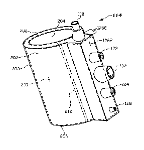
[0035] FIG. ZA illustrates a perspective view of a high-
voltage outer coil 114 in accordance with embodiments provided
herein. As discussed, each coil assembly 106, 108 and 110
includes a high-voltage outer coil 114. The high-voltage
outer coil 114 includes an outer surface 202, an inner surface
204, an upper end surface 206 and a lower end surface 208
(e.g., each outer coil 114 of each coil assembly 106, 108 and
110 has an outer surface, an inner surface, an upper end
surface and a lower end surface).
[0036] A conductive shield 210 (shown in phantom) may
provide shielding to each of the surfaces of high-voltage
outer coil 114 (as described further below). The conductive
shield 210 may be highly electrically conductive so as to
provide a low resistance path to ground for static charge
and/or high voltage levels on the exterior surfaces of high-
voltage outer coil 114. The grounding terminal 128 is
connected to the conductive shield 210 thereby providing a
means of electrically grounding the outer surface of high-
voltage outer coil 114.
[0037] A loop separator region 212 may be included in the
conductive shield 210 across each of the surfaces of high
voltage outer coil 114 on which the conductive shield 210 is
formed. As shown, the loop separator region 212 is formed as
an interruption in the conductive shield 210 (beneath each of
the outer surface 202, the inner surface 204, the upper end
surface 206, and the lower end surface 208 of the high-voltage
outer coil 114). The loop separator region 212 forms a
continuous loop that is devoid of electrically-conductive
material (e.g., an open loop). The inclusion of the loop
12
CA 03102648 2020-12-04
WO 2019/232763
PCT/CN2018/090317
separator region 212 in the conductive shield 210 helps
prevent the creation of loop currents on the surfaces of the
high-voltage outer coil 114.
[0038] In an aspect with broad applicability to
transformers, an improved conductive shield 210 applied to
each of the surfaces of the high-voltage outer coil 114 is
provided.
[0039] Formation of the conductive shield 210 of high-
voltage outer coil 114 is illustrated in FIGS. 2B-2E. FIG. 2B
illustrates a perspective view of a winding 214 that may form
part of the high-voltage outer coil 114. FIG. 2C illustrates a
perspective view of winding 214 having a first insulating
material 216 formed over winding 214. FIGS. 2D and 2E
illustrates a top-side and bottom-side perspective view,
respectively, of winding 214 having conductive shield 210
formed over first insulating material 216.
[0040] With reference to FIG. 2B-2C, in some embodiments,
to form the high-voltage outer coil 114 (FIG. 2A), an outer
surface 218a, an inner surface 218h, an upper end surface 218c
and a lower end surface 218d of winding 214 (shown in FIG. 2B)
may be covered with first insulating material 216 (shown in
FIG. 2C). An outer surface 220a, an inner surface 220b, an
upper end surface 220c and a lower end surface 220d of first
insulating material 216 (shown in FIG. 2C) may be covered with
a conductive shield 210 (shown in FIGS. 2D and 2E). Loop
separator region 212 may be included in conductive shield 210
across each of the surfaces comprising high voltage outer coil
114. As shown, the loop separator region 212 is formed as an
interruption in the conductive shield 210 along each of the
outer surface 220a, the inner surface 220b, the upper end
13
QA 03102648 2020-12-04
WO 2019/232763 PCT/CN2018/090317
surface 220c, and the lower end surface 220d of the first
insulating material 216 of winding 214 of high-voltage outer
coil 114. The loop separator region 212 forms a continuous
loop along each of the surfaces comprising the first
insulating material 216 of high-voltage outer coil 114, and
that is devoid of electrically-conductive material. The
inclusion of the loop separator region 212 in the conductive
shield 210 helps prevent the creation of loop currents on the
surfaces of high-voltage outer coil 114.
[0041] Example conductive shields for high-voltage outer
coil 114 are described below with reference to FIGS. 3A.-3C.
For convenience, only a portion of winding 214 is shown in
FIGS. 3A-3C. It will be understood that conductive shields may
provide shielding for most, if not all, surfaces of the high-
voltage outer coil 114 in some embodiments.
[0042] FIG. aA illustrates a partial cross-sectional side
view of a portion of high-voltage outer coil 114 having a
conductive shield in accordance with embodiments provided
herein. With reference to FIG. 3A, winding 214 of high-voltage
outer coil 114 is covered by the first insulating material 216.
For example, winding 214 may be wound in a cylindrical shape,
forming a winding structure having an outer surface 218a,
inner surface 218b, upper end surface 218c and lower end
surface 218d as shown in FIG. 2B. The first insulating
material 216 may fully cover these surfaces as shown in FIG.
2C. The first insulating material 216 may be an epoxy resin,
polyurethane, polyester, silicone, or the like. Other suitable
insulating materials may be employed. Example resins include
AraduraD HY 926 CH and/or Araldite@ CY 5948 available from
Huntsman Quimica Ltda. of Sao Paulo, Brazil. In some
14
QA 03102648 2020-12-04
WO 2019/232763
PCT/CN2018/090317
embodiments, the resin may be fiberglass reinforced. The
thickness of the first insulating material 216 layer may be
between 6-7 mm although other suitable thickness ranges may be
used.
[0043] A conductive shield 210 is formed over the first
insulating material 216. Specifically, the conductive shield
210 is formed over insulating material 216 on at least a
portion of each surface comprising the high-voltage outer coil
114. For example, as shown in FIGS. 2C-2E, the conductive
shield 210 may be formed over first insulating material 216 on
at least a portion of each of the outer surface 220a, the
inner surface 220b, the upper end surface 220c and the lower
end surface 220d of first insulating material 216 of the high-
voltage outer coil 114.
[0044] In some embodiments, the conductive shield 210 may
be a conductive paint applied to the first insulating material
216. The conductive paint may be comprised of a conductive
metal including one or more of copper, nickel, silver-coated
copper, nickel-silver, and silver. Other suitable conductive
paints may be used. In some embodiments, the conductive paint
may have an electrical resistance between about 0.01 Ohm/sq
in/mil to 1 Ohm/sq in/mil and/or have a thickness of between
about 30 and 500 microns, and in some embodiments between
about 30 and 150 microns, as applied, although other suitable
resistances and/or thickness ranges may be used (wherein "sq
in" is an abbreviation for "square inch" and "mil" is 0.001
inch). The conductive paint may be applied by any suitable
process, such as brushing, rolling, spraying, and dipping.
Moreover, a stencil or mask may be used to form a pattern on
the first insulating material 216, the pattern including a
QA 03102648 2020-12-04
WO 2019/232763
PCT/CN2018/090317
grid pattern, a striped pattern or any other suitable pattern.
In some embodiments, the application of the conductive shield
210 may be done in a manner that ensures its electrical
continuity across each of the surfaces of the high-voltage
outer coil 114 (e.g., each of the outer surface 220a, the
inner surface 220h, the upper end surface 220c and the lower
end surface 220d of first insulating material 216 of the high-
voltage outer coil 114).
[0045] In some embodiments, the conductive shield 210 may
include a loop separator region 212. The loop separator region
212 may be formed by an interruption in the conductive shield
210 on each of the outer surface 220a, the inner surface 220b,
the upper end surface 220c and the lower end surface 220d of
first insulating material 216 of the high-voltage outer coil
114 (FIGS. 2C-2E). In some embodiments, the interruption may
be between 4-6 mm wide, although other suitable width ranges
may be used. The loop separator region 212 forms a continuous
loop that is devoid of any conductive paint (e.g., an open
loop) across all the surfaces comprising the high-voltage
outer coil 114 (extending across each of the outer surface
220a, the inner surface 220b, the upper end surface 220c and
the lower end surface 220d of first insulating material 216 of
the high-voltage outer coil 114 (FIGS. 2C-2E)). The loop
separator region 212 may be provided in one form or another
whether the conductive paint has been applied as a continuous
sheet or as a pattern.
[0046] In some embodiments, a ground connection 310 may be
coupled to the conductive shield 210. For example, in some
embodiments, the ground connection 310 may be a metal plate in
direct contact with the conductive shield 210 or a conductive
16
QA 03102648 2020-12-04
WO 2019/232763
PCT/CN2018/090317
tape formed over or under the conductive shield 210. When the
conductive shield 210 comprises conductive paint, at least a
portion of the ground connection 310 may be placed on top of
or underneath the conductive paint, for example. Other ground
connections may be used. A ground terminal 312 may be attached
to the ground connection 310 to which an external ground lead
or cable may be attached. Ground connection 310 and/or ground
terminal 312 may be formed from any suitable material such as
copper, brass, aluminum or the like. In some embodiments, one
or more of high voltage terminal 118, upper terminal 122,
lower terminal 124, ground terminal 126, and/or tap changer
assembly 132 may be masked during application of the
conductive shield 210.
[0047] A second insulating material 314 may be applied over
the conductive shield 210 and the ground connection 310. As
with the first insulating material 216, the insulating
material may be an epoxy resin, polyurethane, polyester,
silicone, or the like. Other suitable insulating materials
may be employed. Whichever insulating material is employed,
the second insulating material 314 may protect the conductive
shield 210 from humidity, water, pollution, and the like.
[0048] FIG. 3B illustrates a partial cross-sectional side
view of a coil with an alternate example embodiment of a
conductive shield provided herein. With reference to FIG. 3B,
winding 214 of high-voltage outer coil 114 is covered by the
first insulating material 216. For example, a continuous layer
of first insulating material 216 may full cover winding 214.
The first insulating material 216 may cover the outer surface
218a, inner surface 218b, upper end surface 218c and lower end
surface 218 of winding 214 of high-voltage outer coil 114
17
QA 03102648 2020-12-04
WO 2019/232763 PCT/CN2018/090317
(FIGS. 2B-2C). The first insulating material 216 may be an
epoxy resin, polyurethane, polyester, silicone, or the like.
Other suitable insulating materials may be employed. Example
resins include Aradur HY 926 CH and/or Araldite CY 5948
available from Huntsman Quimica Ltda. of Sao Paulo, Brazil. In
some embodiments, the resin may be fiberglass reinforced. The
thickness of the first insulating material 216 may be between
6-7 mm although other suitable thickness ranges may be used.
[0049] In the embodiment of FIG. 3B, conductive shield 210
is formed from a layer of semi-conductive paint 316 and a
layer of conductive paint 317. For example, a layer of semi-
conductive paint 316 may be formed over the first insulating
material 216. The semi-conductive paint 316 may be applied to
the first insulating material 216 over all of the surfaces
comprising the high-voltage outer coil 114. For example, the
semi-conductive paint 316 may be applied over insulating
material 216 on each of the outer surface 220a, the inner
surface 220b, the upper end surface 220c and the lower end
surface 220d of first insulating material 216 of the high-
voltage outer coil 114 (FIG. 2C). The layer of semi-
conductive paint 316 may provide for a uniform electric field
and/or voltage potential across the outer surface 202, the
inner surface 204, the upper end surface 206 and the lower end
surface 208 of the high-voltage outer coil 114 (FIG. 2A).
[0050] Semi-conductive paint 316 may be similar in
composition to conductive paint 317 in that it may be
comprised of a conductive metal including one or more of
copper, nickel, silver-coated copper, nickel-silver, and
silver. Other suitable semi-conductive paint types may be used.
Semi-conductive paint 316 differs from conductive paint 317 in
18
QA 03102648 2020-12-04
WO 2019/232763
PCT/CN2018/090317
that it generally encompasses a higher electrical resistance
range. In some embodiments, the semi-conductive paint 316 may
have an electrical resistance between about 1 kilo-ohm/sq
in/mil to 10 kilo-ohm/sq in/mil and/or a thickness of between
about 10 and 500 microns, and in some embodiments between
about 10 and 50 microns, as applied, although other suitable
electrical resistances and/or thickness ranges may be used.
[0051] After formation of the layer of semi-conductive
paint 316, conductive paint 317 is formed over the layer of
semi-conductive paint 316. For example, the conductive paint
317 may be formed over the semi-conductive paint 316 that was
formed on first insulating material 216, with the conductive
paint 317 covering at least a portion of each of the outer
surface 220a, the inner surface 220b, the upper end surface
220c and the lower end surface 220d of first insulating
material 216 that was covered with semi-conductive paint 316.
Conductive shield 210, which includes conductive paint 317 and
underlying semi-conductive paint 316, is therefore formed on
at least a portion of each of the outer surface 220a, the
inner surface 220b, the upper end surface 220c and the lower
end surface 220d of first insulating material 216 of high-
voltage outer coil 114 (as shown in FIGS. 2C-2E).
[0052] Conductive paint 317 may be comprised of a
conductive metal including one or more of copper, nickel,
silver-coated copper, nickel-silver, and silver. Other
suitable conductive paints may be used. In some embodiments,
the conductive paint 317 may have an electrical resistance
between about 0.01 Ohm/sq in/mil to 1 Ohm/sq in/mil and/or
have a thickness of between about 30 and 500 microns, and in
some embodiments between about 30 and 150 microns, as applied,
19
QA 03102648 2020-12-04
WO 2019/232763 PCT/CN201
8/09031 7
although other suitable resistance and/or thickness ranges may
be used. The semi-conductive paint 316 and/or conductive paint
317 may be applied by any suitable process, such as brushing,
rolling, spraying, and dipping. In some embodiments, a stencil
or mask may be used to form a pattern of conductive paint on
the layer of semi-conductive paint 316 formed over the first
insulating material 216, the pattern including a grid pattern,
a striped pattern or any other suitable pattern. In some
embodiments, the application of the conductive shield 210 may
be done in a manner that ensures its electrical continuity
across each of the surfaces of the high-voltage outer coil 114
(e.g., across each of the outer surface 220a, the inner
surface 220b, the upper end surface 220c and the lower end
surface 220d of first insulating material 216 of the high-
voltage outer coil 114).
[0053] In some embodiments, the conductive shield 210 may
include a loop separator region 212. The loop separator
region 212 is formed as an interruption in the conductive
paint 317 portion of conductive shield 210 on each of the
outer surface 220a, the inner surface 220b, the upper end
surface 220c and the lower end surface 220d of first
insulating material 216 of the high-voltage outer coil 114
(FIGS. 2C-2E). The interruption in the layer of conductive
paint 317 may be between 4-6 mm wide although other suitable
width ranges may be used. The loop separator region 212 forms
a continuous loop that is devoid of any conductive paint 317
across all the surfaces comprising the high-voltage outer coil
114 (extending across each of the outer surface 220a, the
inner surface 220b, the upper end surface 220c and the lower
end surface 220d of first insulating material 216 of the high-
voltage outer coil 114 (FIGS. 2C-2E) and exposing the
CA 03102648 20202-04
WO 2019/232763
PCT/CN2018/090317
underlying semi-conductive paint 316 in the gap region). The
loop separator region 212 may be present in one form or
another whether the conductive paint 317 has been applied as a
continuous layer or as a pattern. In one or more embodiments,
conductive paint 317 may have a resistance that is low enough
to allow the formation of (measurable) current loops on the
surfaces of the high-voltage outer coil 114 if loop separator
region 212 is not employed. Such current loops may cause
heating of and damage to the coil assembly.
[0054] The semi-conductive paint 316 exposed in the loop
separator region 212 in conductive paint 317 helps prevent
leakage of an electric field through the loop separator region
212 during operation of the high-voltage outer coil 114.
Moreover, the higher electrical resistance range of the layer
of the semi-conductive paint 316 helps prevent the formation
of a ground loop within the layer of semi-conductive paint 316
(even though the semi-conductive paint 316 may be present in
the loop separator region 212). In one or more embodiments,
semi-conductive paint 316 may have a resistance that is high
enough to prevent the formation of (measurable) current loops
on the surfaces of the high-voltage outer coil 114.
[0055] In some embodiments, a ground connection 310 may be
coupled to the conductive shield 210. For example, in some
embodiments, the ground connection 310 may be a metal plate in
direct contact with the conductive shield 210 or a conductive
tape formed over or under the conductive shield 210. When the
conductive shield 210 comprises conductive paint, at least a
portion of the ground connection 310 may be placed on top of
or underneath the conductive paint (e.g., on top of semi-
conductive paint 316), for example. Other ground connections
21
QA 03102648 2020-12-04
WO 2019/232763
PCT/CN2018/090317
may be used. A ground terminal 312 may be attached to the
ground connection 310 to which an external ground lead or
cable may be attached. In some embodiments, one or more of
high voltage terminal 118, upper terminal 122, lower terminal
124, ground terminal 128, and/or tap changer assembly 132 may
he masked during application of the conductive shield 210.
[0056] A second insulating material 314 may be applied over
the conductive shield 210 and the ground connection 310. As
with the first insulating material 216, the insulating
material may be an epoxy resin, polyurethane, polyester,
silicone, or the like. Other suitable insulating materials
may be employed. Whichever insulating material is employed,
the second insulating material 314 may protect the conductive
shield 210 from humidity, water, pollution, and the like.
[0057] As mentioned, the combination of the conductive
shield 210 and the ground connection 310 provides for a low
resistance path to ground for static charge and/or high
voltages distributed across the exterior surfaces of the high-
voltage outer coil 114.
[0058] FIG. 3C illustrates a partial cross-sectional side
view of a coil with another alternate example embodiment of a
conductive shield provided herein. With reference to FIG. 3C,
winding 214 of high-voltage outer coil 114 is covered by the
first insulating material 216. For example, a continuous layer
of first insulating material 216 may full cover winding 214.
The first insulating material 216 may cover the outer surface
218a, inner surface 218b, upper end surface 218c and lower end
surface 218d of winding 214 of high-voltage outer coil 114
(FIGS. 28-20). The first insulating material 216 may be an
epoxy resin, polyurethane, polyester, silicone, or the like.
22
QA 03102648 2020-12-04
WO 2019/232763 PCT/CN2018/090317
Other suitable insulating materials may be employed. Example
resins include Aradur HY 926 CH and/or Araldite CY 5948
available from Huntsman Quimica Ltda. of Sao Paulo, Brazil. In
some embodiments, the resin may be fiberglass reinforced. The
thickness of the first insulating material 216 may be between
6-7 mm although other suitable thickness ranges may be used.
[0059] In the embodiment of FIG. 3C, conductive shield 210
is formed from a conductive mesh applied along the first
insulating material 216 and a semi-conductive paint formed
over the conductive mesh. With reference to FIG. 3C, a
conductive mesh 318 is placed over the first insulating
material 216. For example, conductive mesh 318 may be applied
over insulating material 216 on each of the outer surface 220a,
the inner surface 220b, the upper end surface 220c and the
lower end surface 220d of first insulating material 216 of the
high-voltage outer coil 114 (FIG. 20). As mentioned, the first
insulating material 216 may be an epoxy resin, polyurethane,
polyester, silicone, or the like. Other insulating materials
may be employed. In some embodiments, the resin may be
fiberglass reinforced. The thickness of the first insulating
material 216 layer may be between 6-7 mm, although other
suitable thickness ranges may be used.
[0060] Conductive mesh 318 may be comprised of a conductive
material formed into a pattern (e.g., a grid or screen).
Example conductive materials for the conductive mesh 318
include conductive metals such as one or more of copper,
nickel, silver-coated copper, nickel-silver, silver or the
like, although other types of conductive meshes may be used.
In some embodiments, conductive mesh 318 may have an
electrical resistance of between about 0.01 to 1 Ohm/sq cm,
23
CA 031026482024
WO 2019/232763
PCT/CN2018/090317
although other suitable electrical resistance ranges may be
used.
[0061] In some embodiments, semi-conductive paint (not
separately shown) may be used to hold conductive mesh 318 in
place and/or to fill the gaps regions of conductive mesh 318.
The semi-conductive paint applied to the conductive mesh 318
may be comprised of a conductive metal including one or more
of coal powder, copper, nickel, silver-coated copper, nickel-
silver, and silver, although other suitable types of semi-
conductive paint may be used. In some embodiments, the semi-
conductive paint may have an electrical resistance of between
about 1 kilo-ohm/sq in/mil to 10 kilo-ohm/sq in/mil, although
other suitable electrical resistance ranges may be used.
[0062] Once the conductive mesh 318 has been positioned on
the first insulating material 216, semi-conductive paint may
be applied to the conductive mesh 318 by any suitable process,
such as brushing, rolling, spraying, and dipping. The
composite structure of conductive mesh material and semi-
conductive paint serves as conductive shield 210. In some
embodiments, the composite structure may have a thickness of
between about 100 and 500 microns, although other suitable
thickness ranges may be used.
[0063] In some embodiments, the conductive shield 210 may
include a loop separator region 212. The loop separator region
212 may be formed as an interruption in the conductive shield
210 on each of the outer surface 220a, the inner surface 220b,
the upper end surface 220c and the lower end surface 220d of
first insulating material 216 of the high-voltage outer coil
114 (FIGS. 2C-2E). In some embodiments, the interruption may
be between 4-6 mm wide, although other suitable width ranges
24
QA 03102648 2020-12-04
WO 2019/232763 PCT/CN2018/090317
may be used. The loop separator region 212 forms a continuous
loop that is devoid of any conductive mesh across all the
surfaces comprising the high-voltage outer coil 114 (extending
through each of the outer surface 220a, the inner surface 220b,
the upper end surface 220c and the lower end surface 220d of
first insulating material 216 of the high-voltage outer coil
114 (FIGS. 2C-2E)). The loop separator region 212 may be
provided in one form or another whether the conductive mesh
has been applied as a continuous sheet or as a series of mesh
pieces. The loop separator region 212 may include semi-
conductive paint in one or more embodiments.
[0064] In some embodiments, a ground connection 310 may be
coupled to the conductive shield 210. For example, in some
embodiments, the ground connection 310 may be a metal plate in
direct contact with the conductive shield 210 or a conductive
tape formed over or under the conductive shield 210. When the
conductive shield 210 comprises conductive mesh with semi-
conductive paint, at least a portion of the ground connection
310 may be placed on top of or underneath the conductive mesh,
for example. Other ground connections may be used. A ground
terminal 312 may be attached to the ground connection 310 to
which an external ground lead or cable may be attached. In
some embodiments, one or more of high voltage terminal 118,
upper terminal 122, lower terminal 124, ground terminal 128,
and/or tap changer assembly 132 may be masked during
application of the conductive shield 210.
[0065] A second insulating material 314 may be applied over
the conductive shield 210 and the ground connection 310. As
with the first insulating material 216, the insulating
material may be an epoxy resin, polyurethane, polyester,
CA 03102648 2020-12-04
WO 2019/232763 PCT/CN2018/090317
silicone, or the like. Other suitable insulating materials
may be employed. Whichever insulating material is employed,
the second insulating material 314 may protect the conductive
shield 210 from humidity, water, pollution, and the like.
[0066] Now referring to FIG. 4, in some embodiments, a
method 400 of forming a high-voltage outer coil (e.g. high-
voltage outer coil 114) of a dry-type transformer (e.g.,
transformer 100) is provided. The method 400 includes, in 402,
providing a high-voltage outer coil (e.g., winding 214 of FIG.
28) having an outside surface. The outside surface including
an outer surface, an inner surface, an upper end surface and a
lower end surface (e.g., outer surface 218a, inner surface
218b, upper end surface 218c and lower end surface 218d).
[0067] The method 400 further includes, in 404, providing
the outer surfaces of the coil (e.g., winding 214) with a
layer of a first insulating material (e.g., first insulating
material 216 of FIG. 2C). The layer of first insulating
material may fully encapsulate or encase the outer surface,
the inner surface, the upper surface and the lower surface of
the coil. The insulating material, for example, may be an
epoxy resin, polyurethane, polyester, silicone, or the like.
[0068] Further, the method 400 includes, in 406, providing
a conductive shield (e.g., conductive shield 210) over at
least a portion of each of the outer surface, the inner
surface, the upper end surface and the lower end surface of
the coil. The conductive shield may be a conductive paint
(e.g., FIG. ap), a combination of conductive paint overlying
semi-conductive paint (e.g., FIG. 3B), or a composite
structure formed from conductive mesh and semi-conductive
paint (e.g., FIG. 3C). The conductive shield may include a
26
CA 03102648 2020-3.04
W02019/232763 PCT/CN2018/090317
break (e.g., loop separator region 212) which is a continuous
loop-shaped separation in the conductive shield across each of
the surfaces of the coil. This separation may prevent the
formation of loop currents within the conductive shield.
[0069] Moreover, the method 400 includes, in 408, providing
a ground connection (e.g., grounding connection 310) coupled
to the conductive shield. In some embodiments, the ground
connection may be a metal plate in direct contact with the
conductive shield, a conductive tape formed over or under the
conductive shield or the like. A ground terminal may be
attached to the ground connection, and an external ground lead
or cable may be attached thereto.
[0070] Additionally, the method 400 further includes, in
410, providing the coil with a layer of a second insulating
material on the outside surfaces of the coil (e.g., second
insulating material 314). The layer of second insulating
material may fully encapsulate or encase the conductive shield
on the surfaces of the coil. As with the first insulating
material, the second insulating material may be an epoxy resin,
polyurethane, polyester, silicone, or the like.
[0071] The embodiments described with reference to FIGS.
1A-4 describe use of a conductive shield 210 and/or a loop
separator region 212 with a high-voltage outer coil 114. In
some embodiments, a conductive shield 210 (with or without a
loop separator region 212) similarly may be provided for the
low-voltage inner coil 112. Additionally, in some embodiments,
the outer coil 114 may be a low-voltage coil and the inner
coil 112 may be a high-voltage coil. More generally, a coil
assembly may include a first, inner coil and second, outer
coil (e.g., concentrically arranged) or single coil. In some
27
CA 03102648 20202-04
W02019/232763 PCT/CN2018/090317
embodiments, the first, inner coil may be a low-voltage coil
and the second, outer coil may be a high-voltage coil, while
in other embodiments, the first, inner coil may be a high-
voltage coil and the second, outer coil may be a low-voltage
coil. Either or both of the inner and outer coils may have a
conductive shield and/or a loop separator region as described
herein.
[0072] In some embodiments, the conductive shield may be
configured to overlap itself while maintaining a loop
separator region. Such an arrangement may be used, for example,
in very high electric field applications. FIG. 5A illustrates
a partial cross-sectional side view of a portion of the
conductive shield 210 of FIG. aA in which the conductive
shield 210 overlaps itself in accordance with embodiments
provided herein. With reference to FIG. 5A, an insulating
material 502, such as an insulating foil, may be placed over a
first portion 210a of conductive shield 210 so that a second
portion 210b of conductive shield 210 overlaps the first
portion 210a. For example, in the embodiment of FIG. 3A in
which the conductive shield 210 is a conductive paint, the
first portion 210a of conductive shield 210 may be applied,
and the insulating material 502 may be positioned over the
first portion 210a of conductive shield 210 prior to
application of the second portion 210b of the conductive
shield 210. A gap (e.g., loop separator region 212) may be
maintained. In some embodiments, a spacer material or mesh
(not shown) may be employed, in addition to or in place of the
insulating material 502, to allow subsequent insulating
material (e.g., resin) applied to the conductive shield 210 to
enter and insulate between the first portion 210a and second
portion 210b of conductive shield 210. In one or more
28
CA 03102648 2020-12-04
WO 2019/232763
PCT/CN2018/090317
embodiments, the first portion 210a may overlap the second
portion 210b of conductive shield 210 by about 8-12 mm,
although other overlap amounts may be used. Example
insulating materials include polyurethane, polyester, silicone,
and the like.
[0073] A similar overlap in conductive shield 210 may be
employed when conductive shield 210 includes an underlying
semi-conductive paint layer (FIG. 3B) or when conductive
shield 210 includes a conductive mesh (FIG. 3C). For example,
FIG. 53 illustrates a partial cross-sectional side view of a
portion of the conductive shield 210 of FIG. 3B in which the
conductive shield 210 overlaps itself and FIG. 5C illustrates
a partial cross-sectional side view of a portion of the
conductive shield 210 of FIG. 3C in which the conductive
shield 210 overlaps itself in accordance with embodiments
provided herein. In the embodiment of FIG. 53, a first portion
317a of conductive paint 317 overlies the layer of semi-
conductive paint 316 and underlies insulating material 502 and
a second portion 317b of conductive paint 317 while
maintaining a gap (e.g., loop separator region 212). Likewise,
in the embodiment of FIG. 5C, a first portion 210a of
conductive shield 210 underlies insulating material 502 and a
second portion 210b of conductive shield 210 while maintaining
a gap (e.g., loop separator region 212).
[0074] While the
present disclosure is described primarily
with regard to submersible dry-type transformers, it will be
understood that the disclosed conductive shields may also be
employed with other types of transformers or coil assemblies,
such as inductors.
29
CA 03102648 2020-12-04
WO 2019/232763 PCT/CN2018/090317
[0075] The foregoing description discloses only example
embodiments. Modifications of the above-disclosed assemblies
and methods which fall within the scope of this disclosure
will be readily apparent to those of ordinary skill in the art.
For example, although the examples discussed above are
illustrated for dry-type transformers, other embodiments in
accordance with this disclosure may be implemented for other
devices. This disclosure is not intended to limit the
invention to the particular assemblies and/or methods
disclosed, but, to the contrary, the intention is to cover all
modifications, equivalents, and alternatives falling within
the scope of the claims.