Note: Descriptions are shown in the official language in which they were submitted.
CA 03102831 2020-12-04
WO 2019/236510
PCT/US2019/035283
STATIC TRANSFER SWITCH WITH RESONANT TURN-OFF
BACKGROUND
[0001] The present inventions relate generally to static transfer switches,
and
more particularly, to turning off the switches therein.
[0002] A static transfer switch (STS) is a known type of electrical
component that
is used to distribute electric power to sensitive loads. For example, static
transfer
switches are commonly used to supply electric power to data centers or other
industrial plants or facilities where constant, reliable power is necessary.
[0003] A static transfer switch is used to switch between multiple power
sources
to supply a load with electric power. For example, one power source, such as
an
electric grid, may be a primary power source, and a second power source, such
as a
generator, may be a backup power source. Both power sources are supplied to
the
static transfer switch which supplies power to the load. During normal
conditions,
the static transfer switch monitors the primary power source and a backup
power
source, and supplies power from the primary power source to the load. When the
power from the primary power source deteriorates, the static transfer switch
switches
to the backup power source to supply the load. Such switching is designed to
happen quickly enough that the load is not affected by the switch between
power
supply sources.
[0004] In order to achieve the desired switching speed and reliability,
static
transfer switches use "static" switching, meaning that solid-state power
electronics
are used to switch between power sources However, even with the use of solid-
state power electronics, switching speed is a concern with static transfer
switches.
For example, deterioration in the primary power source can happen suddenly,
and it
is important to switch away from a deteriorating primary power source quickly.
That
is, many of the electrical components, for example in a data center. are
particularly
sensitive to power supply fluctuations. Moreover, the timing of the switching
between the two power sources must be seamless. Thus, for example. it is
undesirable for a delay in disconnecting a power source to result in a spike
in power
by temporarily having multiple power sources connected to the load or to allow
a gap
in power by temporarily having no power source connected to the load.
Therefore, it
1
is important in a static transfer switch to be able to disconnect a power
source as quickly as
possible when switching between power sources.
SUMMARY
[0005] A static transfer switch is described that turns off a power
source is less than
half an AC cycle. This allows the static transfer switch to switch between two
power
sources quickly to maintain adequate electric power to sensitive loads. The
circuit includes
two main switches and two resonant switches. At least one of the resonant
switches is
turned on to turn off a main switch.
According to an aspect of the present invention, there is provided a static
transfer switch, comprising:
first and second main switches, the first and second main switches being
arranged
anti-parallel to each other, the first and second main switches being turned
on to conduct
electric power by supplying a first gate signal to each of the first and
second main switches,
the first and second main switches being turned off to stop conducting the
electric power by
reversing voltage across the first and second main switches;
a capacitor and an inductor arranged in parallel with the first and second
main
switches;
first and second resonant switches arranged in series with the capacitor and
the
inductor;
wherein a second gate signal is supplied to at least one of the first and
second
resonant switches to apply a reverse voltage across one of the first and
second main
switches to turn off the one of the first and second main switches.
BRIEF DESCRIPTION OF SEVERAL VIEWS OF THE DRAWINGS
[0006] The invention may be more fully understood by reading the
following
description in conjunction with the drawings, in which:
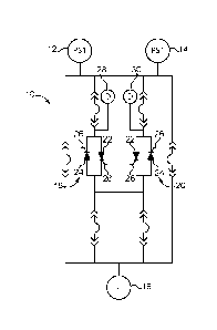
[0007] Figure 1 is a circuit diagram of static transfer switch;
2
Date Recue/Date Received 2021-02-26
[0008] Figure 2 is a circuit diagram of a resonant turn-off circuit;
[0009] Figure 3 is a chart showing one of the thyristors of Figure 2
being turned off;
[0010] Figure 4 is an expanded chart of Figure 3;
[0011] Figure 5 is a circuit diagram of another resonant turn-off
circuit;
[0012] Figure 6 is a showing one of the thyristors of Figure 5 being
turned off;
[0013] Figure 7 is an expanded chart of Figure 6;
DETAILED DESCRIPTION
[0014] Referring now to the figures, and particularly Figure 1, a
circuit diagram is
shown for a static transfer switch 10. As shown, the static transfer switch 10
is supplied
with a first power source 12 and a second power source 14. The output of the
static
transfer switch 10 is connected to a load 16, such as a data center. Switching
between the
power sources 12, 14 is accomplished through the use of corresponding sets
18,20 of first
and second main switches 22, 24. Preferably, the main switches 22, 24 are
thyristors or
gate turn-off thyristors (GTO). The main switches 22, 24 are arranged anti-
parallel to each
other, such that when AC power is supplied to the switches 22, 24 from the
power source
12, 14, and the main switches 22, 24 are turned on, positive polarity half
cycles of the AC
power are conducted by
2a
Date Recue/Date Received 2021-02-26
CA 03102831 2020-12-04
WO 2019/236510
PCT/US2019/035283
the first main switch 22 and negative polarity half cycles of the AC power are
conducted by the second main switch 24.
[0015] The main switches 22, 24 are turned on to conduct electric power by
supplying a first gate 26 signal to the gates 26 of the first and second main
switches
22, 24. Once turned on, each of the main switches 22, 24 typically continues
to
conduct electric power even after the first gate 26 signal is no longer being
supplied
to the gates 26 of the switches 22, 24. In order to turn off the main switches
22, 24
to stop each of the main switches 22, 24 from conducting electric power, the
voltage
applied across the main switch 22, 24 may be reversed. When the power source
12,
14 is an AC power source, a voltage reversal suitable to turn off the main
switches
22, 24 occurs at every half cycle of the AC power source. For example, if the
main
switches 22, 24 are turned on by gate 26 signals (and the gate 26 signal is
immediately removed), a positive polarity first half cycle will conduct
through the first
main switch 22. Then, when the AC cycle reaches the zero crossing, the first
main
switch 22 will turn off due to the reversal of polarity. The negative polarity
second
half cycle then conducts through the second main switch 24. Once the AC cycle
again reaches the zero crossing, the second main switch 24 turns off due to
the
reversal of polarity.
[0016] In order to prevent the main switches 22, 24 from naturally turning
off at
each zero crossing of the AC power source, a constant or constantly pulsed
first gate
26 signal may be supplied to the gates 26 of one set 18, 20 of main switches
22. 24
during the time that electric power is desired from the power source 12, 14
connected to the set 18, 20 of switches 22, 24. Thus, when electric power is
no
longer desired from the first power source 12, the first gate 26 signal is
removed
from the first set 18 of main switches 22, 24, and the first gate 26 signal is
applied to
the second set 20 of main switches 22, 24. As a result, the main switches 22,
24 in
the first set 18 naturally turn off during the next two AC half cycles, and
the main
switches 22, 24 in the second set 20 turn on to conduct electric power from
the
second power source 14 to the load 16.
[0017] In order to determine when to switch between power sources 12, 14,
first
detectors 28, 30 may be provided to monitor the electric performance of the
first and
second power sources 12, 14. Thus, when the first detector 28 for the first
power
source 12 senses a deterioration of performance in the first power source 12,
the
first set 18 of main switches 22, 24 are turned off by removing the first gate
26 signal
3
CA 03102831 2020-12-04
WO 2019/236510
PCT/US2019/035283
and the second set 20 of main switches 22, 24 are turned on to supply power
from
the second power source 14. Since it is desirable to only supply electric
power to
the load 16 from one power source 12, 14 at a time, it may be necessary to
wait to
turn on the second set 20 of main switches 22, 24 until the AC power of the
first
power source 12 cross zero once or twice to ensure that both switches 22, 24
in the
first set 18 have been turned off. Thus, switching time may require one half
or one
complete AC cycle. It is understood that where the power sources 12, 14 have
multiple phases, each phase of each power source 12, 14 will be controlled by
one
set 18, 20 of the main switches 22, 24. Thus, where three phase power is used
with
two power sources 12, 14, a total of six sets 18, 20 of main switches 22, 24
would be
used.
[0018] Turning to Figure 2, a circuit diagram is shown for reversing the
voltage
across at least one of the main switches 22, 24 before an AC polarity reversal
would
otherwise turn off the switch 22. 24 after the gate 26 signal has been stopped
Thus,
the switch 22, 24 can be turned off quickly without having to wait for the AC
power to
reach a zero crossing. As shown, the circuit is provided with at least one
capacitor
32, 34 and an inductor 36. The capacitors 32, 34 and inductor 36 are arranged
parallel with the first and second main switches 22, 24. First and second
resonant
switches 38, 40 are also provided which are arranged in series with the
capacitors
32, 34 and inductor 36 and arranged in parallel with main switches 22, 24.
[0019] When it is desired to turn off the main switches 22, 24, the first
gate 26
signal is removed from the gates 26 of the main switches 22, 24 as described
above.
A second gate 42 signal is then also supplied to the gate 42 of at least one
of the
resonant switches 38, 40 to apply a reverse voltage across the conducting main
switch 22, 24 to turn off the conducting main switch 22, 24 before the AC
polarity
change would naturally turn off the conducting main switch 22, 24. For
example, if
the AC power source 12 is supplying a positive polarity half cycle when it is
desired
to turn off the main switches 22, 24, the first main switch 22 will be
conducting
electrical power to the load 16 when the first gate 26 signal is removed.
Since the
voltage is reversed relative to the second main switch 24, the second main
switch 24
will not be conducting when the first gate 26 signal is removed and will
remain off
once the AC cycle reverses again since the first gate 26 signal has been
removed.
Thus, no extra steps are needed to turn off the second main switch 24.
4
CA 03102831 2020-12-04
WO 2019/236510
PCT/US2019/035283
[00201 Continuing with the example, when the second gate 42 signal is
supplied
to the first resonant switch 38, the charge in the first capacitor 32 is
released and a
resonant frequency is generated between the first capacitor 32 and the
inductor 36.
The resonant frequency is much higher than the frequency of the AC power
source 12 and causes a voltage reversal across the first main switch 22 to
turn off
the first main switch 22 well before the AC power source 12 would turn off the
first
main switch 22 itself by crossing zero. Preferably, a second detector 44 is
provided
to monitor the polarity of the power source 12 supplied to the main switches
22, 24.
Thus, if the polarity is positive, the second gate 42 signal will be supplied
to the first
resonant switch 38 to turn off the first main switch 22, and if the polarity
is negative,
the second gate 42 signal will be supplied to the second resonant switch 40 to
turn
off the second main switch 24. It is possible that the first 28, 30 and second
44
detectors may be combined.
(0021] Although thyristors or GTOs are preferred in a static transfer
switch 10 for
the main switches 22, 24 because of the performance requirements of the main
switches 22, 24. The resonant switches 38, 40 may not need to satisfy the same
performance requirements since the resonant switches 38, 40 are only used
intermittently. Therefore, the resonant switches 38, 40 may be thyristors,
gate turn-
off thyristors (GTO), insulated-gate bipolar transistors (IGBT), or metal-
oxide-
semiconductor field-effect transistors (MOSFET). It may also be possible for
the
resonant switches 38, 40 to have lower capacity ratings than the main switches
22,
24.
[0022] Preferably, power supplies 46, 48 are connected to the capacitors
32, 34
to pre-charge the capacitors 32, 34 and provide a maintenance charge
thereafter.
As shown in Figure 2, where two capacitors 32. 34 are used with one being in
series
with each of the resonant switches 38, 40, it may be desirable to have two
power
supplies 46, 48 with each one connected to one of the capacitors 32, 34.
Because
each of capacitors 32, 34 is used to turn off a different main switch 22, 24,
opposite
charges may be applied to each of the capacitors 32, 34 to provide the
appropriate
voltage reversal needed to turn off each of the main switches 22, 24. It may
also be
possible to combine the power supplies 46, 48 with two DC outputs.
[0023] A resistor 50 may also be arranged in parallel with the capacitor
32, 34
and inductor 36. Preferably, the resistor 50 is a metal-oxide varistor 50. The
resistor 50 reduces load on the circuit by absorbing the resonant current flow
after a
CA 03102831 2020-12-04
WO 2019/236510
PCT/US2019/035283
main switch 22, 24 has been turned off by the corresponding resonant switch
38, 40,
capacitor 32, 34, and inductor 36.
[0024] Turning to Figures 3 and 4, a chart is shown of a resonant switch
38, 40
turning off one of the main switches 22, 24. Figure 3 shows a longer time
frame of
the event, while Figure 4 enlarges the actual switching event. As shown,
current 52
through the main switch 22, 24 follows an AC cycle. In this example, it is
decided to
turn off the main switch 22, 24 at about the peak of the AC cycle. Thus,
without the
resonant switch 38. 40 circuit to turn off the main switch 22, 24 early, the
main switch
22, 24 would not turn off naturally due to the AC cycle reversal for about
twice as
long. As further shown, when the resonant switch 38, 40 is turned on, the
resonant
current 54 is released which causes a sudden reversal 56 in the voltage 58
across
the main switch 22, 24. As explained above, this causes the main switch 22, 24
to
turn off and stop conducting electric power. This is seen in Figures 3 and 4
where
the main switch current 52 suddenly drops 60 to zero. The resonant current 54
lasts
for a relatively short time before it is dissipated 62 through the varistor 50
when the
varistor current 64 increases. After the main switch 22, 24 is turned off, a
temporary
voltage spike 66 occurs across the switch 22, 24. Thereafter, the voltage 58
across
the switch 22, 24 follows 68 the AC cycle of the power source 12.
[0025] Turning to Figure 5, it may also be possible to use a single
capacitor 70 in
the circuit instead of two capacitors 32, 34 as used in Figure 2. In this
case, a single
power supply 72 to charge the capacitor 70 will be used. It may be desirable
for the
power supply 72 to alternate the charge of the capacitor 70 corresponding to
the
polarity of the power source 12.
[0026] Figures 6 and 7 are charts representing a resonant switch 38, 40 of
Figure 5 turning off the main switch 22, 24. When the resonant switch 38, 40
is
turned on, and initial spike 74, 76 in the main switch current 52 and the
resonant
current 54 may occur. Thereafter, the resonant current 54 causes a voltage
reversal 56 across the main switch 22, 24 to turn off the main switch 22, 24.
The
resonant current 54 is dissipated through the varistor 50 as the current 64
through
the varistor 50 increases. After the main switch 22, 24 is turned off, a
temporary
voltage spike 66 occurs across the main switch 22, 24. Thereafter, the voltage
58
across the switch 22, 24 follows 68 the AC cycle of the power source 12.
[0027] While preferred embodiments of the inventions have been described,
it
should be understood that the inventions are not so limited, and modifications
may
6
CA 03102831 2020-12-04
WO 2019/236510
PCT/US2019/035283
be made without departing from the inventions herein. While each embodiment
described herein may refer only to certain features and may not specifically
refer to
every feature described with respect to other embodiments, it should be
recognized
that the features described herein are interchangeable unless described
otherwise;
even where no reference is made to a specific feature. It should also be
understood
that the advantages described above are not necessarily the only advantages of
the
inventions, and it is not necessarily expected that all of the described
advantages will
be achieved with every embodiment of the inventions. The scope of the
inventions is
defined by the appended claims, and all devices and methods that come within
the
meaning of the claims, either literally or by equivalence; are intended to be
embraced therein.