Note: Descriptions are shown in the official language in which they were submitted.
CA 03103295 2020-12-09
WO 2020/055732
PCT/US2019/050178
FLOW CELLS AND METHODS RELATED TO SAME
CROSS-REFERENCE TO RELATED APPLICATIONS
[0001] This
Patent Application claims priority to U.S. Provisional Patent Application No.
62/731,785, filed September 14, 2018, and entitled Flow Cells and Methods
Related to Same.
The entire contents of the aforementioned application is hereby incorporated
herein by reference.
BACKGROUND
[0001] Various protocols in biological or chemical research involve performing
a large number
of controlled reactions on local support surfaces or within predefined
reaction chambers. The
designated reactions may then be observed or detected and subsequent analysis
may help identify
or reveal properties of substances involved in the reaction. For example, in
some multiplex
assays, an unknown analyte having an identifiable label (e.g., fluorescent
label) may be exposed
to thousands of known probes under controlled conditions. Each known probe may
be deposited
into a corresponding well of a microplate. Observing any chemical reactions
that occur between
the known probes and the unknown analyte within the wells may help identify or
reveal
properties of the analyte. Other examples of such protocols include known DNA
sequencing
processes, such as sequencing-by-synthesis (SBS) or cyclic-array sequencing.
[0002] In some conventional fluorescent-detection protocols, an optical system
is used to direct
an excitation light onto fluorescently-labeled analytes and to also detect the
fluorescent signals
that may be emitted from the analytes. However, such optical systems can be
relatively
expensive and involve a relatively large benchtop footprint. For example, such
optical systems
may include an arrangement of lenses, filters, and light sources.
[0003] In other proposed detection systems, the controlled reactions occur on
local support
surfaces or within predefined reaction chambers of a flow cell that does not
involve a large
optical assembly to detect the fluorescent emissions. The flow cell includes
an electronic solid-
state light detector device or imager (e.g., a complementary metal-oxide-
semiconductor (CMOS)
light detector device or a charged-coupled device (CCD) light detector device)
positioned
adjacent (e.g., beneath) the support surfaces/chambers to detect light
emissions from the
reactions. However, such proposed solid-state imaging systems may have some
limitations. For
example, flow cells of such systems may be designed as a single use consumable
item.
1
CA 03103295 2020-12-09
WO 2020/055732 PCT/US2019/050178
Accordingly, it may be beneficial for the flow cell to be a small and
inexpensive device. In a
relatively small flow cell, it may be beneficial to utilize as much of the
biosensor active area of
the light detection device as possible and/or provide as large as a biosensor
active area as
possible.
[0004] Many current flow cell designs do not allow for full utilization of the
biosensor active
area as a lid portion of the flow cells is coupled to the active area, thereby
rendering such area
inaccessible to a reagent solution (e.g., a solution with fluorescently-
labeled molecules) and/or
preventing the area from including reaction sites (e.g., including analytes).
Further, the
biosensor active area is often provided by a single sensor, and relatively
large sensors with
relatively large biosensor active areas are costly. Many current flow cell
designs also provide for
only a limited number of wiring configurations to the light detection devices.
BRIEF DESCRIPTION
[0005] In one aspect of the present disclosure, a flow cell is provided. The
flow cell includes a
support frame comprising a top side, a back side and at least one cavity
extending from the top
side toward the bottom side. The flow cell also includes at least one light
detection device
disposed within the at least one cavity comprising an active area and a top
surface. The flow cell
further includes a support material disposed within the at least one cavity
between the support
frame and the periphery of the at least one light detection device coupling
the support frame and
the at least one light detection device together. The flow cell also includes
a lid extending over
the at least one light detection device and coupled to the top side of the
support frame about the
periphery of the at least one light detection device. The lid and at least the
top surface of the at
least one light detection device form a flow channel therebetween.
[0006] In some examples, the support frame further comprises at least one
electrically
conductive via extending from the top side to the bottom side. In some such
examples, the at
least one light detection device comprises at least one solid-state light
detection device including
a base wafer portion, a plurality of light sensors, device circuitry
electrically coupled to the light
sensors to transmit data signals based on photons detected by the light
sensors, and a plurality of
light guides associated with the plurality of light sensors. In some such
examples, the device
circuitry of the at least one solid-state light detection device is
electrically coupled to the at least
one electrically conductive via at the top side of the support frame.
2
CA 03103295 2020-12-09
WO 2020/055732 PCT/US2019/050178
[0007] In some examples, the lid is indirectly coupled to the top side of the
support frame. In
some examples, the at least one cavity comprises a cavity with a plurality of
light detection
devices disposed therein. In some such examples, the plurality of light
detection devices
comprises distinct light detection devices that are spaced from each other,
and the support
material further extends between adjacent light detection devices. In some
other such examples,
the plurality of light detection devices comprises at least two integral light
detection devices, and
the support material extends between the support frame and the periphery of
the at least two
integral light detection devices.
[0008] In some examples, the at least one light detection device comprises a
plurality of light
detection devices. In some such examples, the at least one cavity comprises a
plurality of
cavities, and each light detection device of the plurality of light detection
devices is disposed in a
differing cavity of the support frame. In some examples, the at least one
light detection device
comprises at least one solid-state light detection device including a base
wafer portion, a
plurality of light sensors, device circuitry electrically coupled to the light
sensors to transmit data
signals based on photons detected by the light sensors, and a plurality of
light guides associated
with the plurality of light sensors. In some such examples, the at least one
cavity extends
through the support frame from the top side to the bottom side, the device
circuitry comprises
vias extending through the base wafer portion, and the flow cell further
comprises electrical
contacts that are at least partially disposed along the back side of the
support frame and
electrically coupled to the vias. In some other such examples, the at least
one light detection
device further comprises a reaction structure disposed over the plurality of
light guides that
forms the top surface thereof, and the reaction structure comprises a
plurality of nanowells
positioned within the active area.
[0009] In some examples, the at least one cavity extends only partially
through the support
frame from the top side toward the bottom side. In some examples, the at least
one light
detection device comprises at least one complementary metal-oxide
semiconductor (CMOS)
light sensor.
[0010] In some examples, the flow channel extends over the entirety of the
active area of the at
least one light detection device.
[0011] In another aspect of the present disclosure, a method is provided. The
method includes
attaching a top surface of a support frame and a planar support surface of a
substrate, the support
3
CA 03103295 2020-12-09
WO 2020/055732 PCT/US2019/050178
frame comprising at least one cavity extending from the top side to a bottom
side thereof The
method further includes positioning at least one light detection device within
the at least one
cavity such that a top side thereof is positioned on the planar support
surface of the substrate and
an edge portion of the cavity extends between the support frame and the
periphery of the at least
one light detection device, the at least one light detection device comprising
an active area and a
top surface. The method also includes filling the edge portion of the cavity
with a support
material to couple the support frame and the at least one light detection
device together. The
method further includes detaching the support frame and the substrate. The
method also includes
attaching a lid to the top side of the support frame about the periphery of
the at least one light
detection device to form a flow cell, the lid extending over the at least one
light detection device
and forming a flow channel between the lid and at least the top surface of the
at least one light
detection device.
[0012] In some examples, the at least one light detection device comprises at
least one solid-
state light detection device including a base wafer portion forming a back
side, a plurality of
light sensors, device circuitry electrically coupled to the light sensors
coupled to transmit data
signals based on photons detected by the light sensors, and a plurality of
light guides associated
with the plurality of light sensors, and the support frame further comprises
at least one
electrically conductive via extending from the top side to the bottom side,
and the method further
comprises electrically coupling the device circuitry of the at least one solid-
state light detection
device to the at least one electrically conductive via at the top side of the
support frame.
[0013] In some examples, the at least one light detection device comprises at
least one solid-
state light detection device including a base wafer portion forming a back
side, a plurality of
light sensors, device circuitry electrically coupled to the light sensors
coupled to transmit data
signals based on photons detected by the light sensors, and a plurality of
light guides associated
with the plurality of light sensors, the device circuitry comprises vias
extending through the base
wafer portion to the back side thereof, and the method further comprises
electrically coupling
contacts that are at least partially disposed along the back side of the
support frame to the vias at
the back side of the base wafer portion.
[0014] In some examples, the method further comprises forming a reaction
structure on the at
least one light detection device prior to attaching the lid, the reaction
structure forming the top
surface of the at least one light detection device and comprising a plurality
of nanowells
4
CA 03103295 2020-12-09
WO 2020/055732 PCT/US2019/050178
positioned within the active area. In some such examples, detaching the
support frame and the
substrate exposes a recessed top side of the support material that extends
below and between the
top side of the support frame and a top portion of the at least one light
detection device, the
reaction structure extends over the recessed top side of the support material
and the top side of
the top side of the support frame, and the reaction structure forms a planar
top surface from
which the plurality of nanowells extend.
[0015] In some examples, the method further comprises obtaining the at least
one light
detection device, and the obtaining the at least one light detection device
comprises dicing at
least one complementary metal-oxide semiconductor (CMOS) light sensor from a
plurality of
integral CMOS light sensors.
[0016] In some examples, the flow channel extends over the entirety of the
active area of the at
least one light detection device.
[0017] In another aspect of the present disclosure, another method is
provided. The method
includes depositing a first support material on a bottom portion of at least
one cavity of a support
frame, the at least one cavity extending only partially through the support
frame from a top side
thereof toward a bottom side thereof. The method further includes positioning
at least one light
detection device within the at least one cavity and over the deposited first
support material such
that an edge portion of the at least one cavity extends between the support
frame and the
periphery of the at least one light detection device, the at least one light
detection device
comprising an active area and a top surface. The method also includes filling
the edge portion of
the cavity with a second support material. The method further includes
attaching a lid to the top
side of the support frame about the periphery of the at least one light
detection device to form a
flow cell, the lid extending over the at least one light detection device and
forming a flow
channel between the lid and at least the top surface of the at least one light
detection device.
[0018] In some examples, the flow channel extends over the entirety of the
active area of the at
least one light detection device.
[0019] It should be appreciated that all combinations of the foregoing aspects
and additional
concepts discussed in greater detail below (provided such concepts are not
mutually inconsistent)
are contemplated as being part of the inventive subject matter and to achieve
the advantages
disclosed herein.
CA 03103295 2020-12-09
WO 2020/055732 PCT/US2019/050178
[0020] These and other objects, features and advantages of this disclosure
will become apparent
from the following detailed description of the various aspects of the
disclosure taken in
conjunction with the accompanying drawings.
DRAWINGS
[0021] These and other features, aspects, and advantages of the present
disclosure will become
better understood when the following detailed description is read with
reference to the
accompanying drawings, which are not necessarily drawn to scale and in which
like reference
numerals represent like aspects throughout the drawings, wherein:
[0022] FIG. 1 illustrates, in one example, a cross-section of a light
detection device, in
accordance with one or more aspects of the present disclosure.
[0023] FIG. 2 illustrates, in one example, a cross-section another light
detection device, in
accordance with one or more aspects of the present disclosure.
[0024] FIG. 3 illustrates, in one example, a support structure comprised of a
support frame and
a substrate for forming a flow cell, in accordance with one or more aspects of
the present
disclosure.
[0025] FIG. 4 illustrates, in one example, positioning a light detection
device within a cavity of
the support structure of FIG. 3, in accordance with one or more aspects of the
present disclosure.
[0026] FIG. 5 illustrates, in one example, a cross-section of a light
detection device positioned
within a cavity of the support structure of FIG. 3, in accordance with one or
more aspects of the
present disclosure.
[0027] FIG. 6 illustrates, in one example, a cross-section of a light
detection device positioned
within a cavity of another support structure, in accordance with one or more
aspects of the
present disclosure.
[0028] FIG. 7 illustrates, in one example, a cross-section of a light
detection device positioned
within a cavity of another support structure, in accordance with one or more
aspects of the
present disclosure.
[0029] FIG. 8 illustrates, in one example, a cross-section of a light
detection device positioned
within a cavity of another support structure, in accordance with one or more
aspects of the
present disclosure.
6
CA 03103295 2020-12-09
WO 2020/055732 PCT/US2019/050178
[0030] FIG. 9 illustrates, in one example, filling a cavity extending about
the periphery of the
light detection device positioned within the cavity of the support structure
of FIG. 4 with filling
material, in accordance with one or more aspects of the present disclosure.
[0031] FIG. 10 illustrates, in one example, removal of the substrate from the
support frame of
the support structure of FIG. 4, in accordance with one or more aspects of the
present disclosure.
[0032] FIG. 11A illustrates, in one example, a cross-section of a plurality of
light detection
devices coupled within a plurality of cavities of the support frame of FIG. 4
with the substrate
removed, in accordance with one or more aspects of the present disclosure.
[0033] FIG. 11B illustrates, in one example, a top view of the plurality of
light detection
devices coupled within the cavities support frame of FIG. 11A, in accordance
with one or more
aspects of the present disclosure.
[0034] FIG. 12A illustrates, in one example, a cross-section of a plurality of
light detection
devices coupled within a cavity of a support frame with a substrate removed,
in accordance with
one or more aspects of the present disclosure.
[0035] FIG. 12B illustrates, in one example, a top view of the plurality of
light detection
devices coupled within the cavity of the support frame of FIG. 12A, in
accordance with one or
more aspects of the present disclosure.
[0036] FIG. 13A illustrates, in one example, a cross-section of a plurality of
light detection
devices coupled within another cavity of a support frame with a substrate
removed, in
accordance with one or more aspects of the present disclosure.
[0037] FIG. 13B illustrates, in one example, a top view of the plurality of
light detection
devices coupled within the cavity of the support frame of FIG. 13A, in
accordance with one or
more aspects of the present disclosure.
[0038] FIG. 14 illustrates, in one example, a cross-section of a plurality of
light detection
devices coupled within cavities of another support frame in accordance with
one or more aspects
of the present disclosure.
[0039] FIG. 15A illustrates, in one example, a cross-section of a light
detection device and
filling material within a cavity of a support frame, in accordance with one or
more aspects of the
present disclosure.
7
CA 03103295 2020-12-09
WO 2020/055732 PCT/US2019/050178
[0040] FIG. 15B illustrates, in one example, a cross-section of the light
detection device and
filling material within the cavity of the support frame of FIG. 15A with a
reaction structure
positioned thereon, in accordance with one or more aspects of the present
disclosure.
[0041] FIG. 16A illustrates, in one example, a cross-section of an
intermediate flow cell device
including a plurality of light detection devices coupled within a plurality of
cavities of a support
frame, in accordance with one or more aspects of the present disclosure.
[0042] FIGS. 16B-16D illustrate, in one example, formation of backside
contacts on the
intermediate flow cell device of FIG. 16A.
[0043] FIG. 17A illustrates, in one example, a cross-section of another
intermediate flow cell
device including a plurality of light detection devices coupled within a
plurality of cavities of a
support frame, in accordance with one or more aspects of the present
disclosure.
[0044] FIGS. 17B and 17C illustrate, in one example, formation of backside
contacts on the
intermediate flow cell device of FIG. 17A.
[0045] FIG. 18A illustrates, in one example, a cross-section of another
intermediate flow cell
device including a plurality of light detection devices coupled within a
plurality of cavities of a
support frame, in accordance with one or more aspects of the present
disclosure.
[0046] FIGS. 18B and 18C illustrate, in one example, formation of backside
contacts on the
intermediate flow cell device of FIG. 18A.
[0047] FIG. 19A illustrates, in one example, a cross-section of another
intermediate flow cell
device including a plurality of light detection devices coupled within a
plurality of cavities of a
support frame, in accordance with one or more aspects of the present
disclosure.
[0048] FIG. 19B and 19C illustrate, in one example, formation of backside
contacts on the
intermediate flow cell device of FIG. 19A.
[0049] FIG. 20 illustrates, in one example, a plurality of flow cells formed
via the intermediate
flow cell device of FIG. 19C, in accordance with one or more aspects of the
present disclosure.
[0050] FIG. 21 illustrates, in one example, a flow channel and active area of
a light detection
device of a flow cell of FIG. 20, in accordance with one or more aspects of
the present
disclosure.
[0051] FIG. 22 illustrates, in one example, a plurality of distinct flow cells
that may be formed
from the plurality of flow cells of FIG. 20, in accordance with one or more
aspects of the present
disclosure.
8
CA 03103295 2020-12-09
WO 2020/055732 PCT/US2019/050178
DETAILED DESCRIPTION
[0052] Aspects of the present disclosure and certain examples, features,
advantages, and details
thereof, are explained more fully below with reference to the non-limiting
examples illustrated in
the accompanying drawings. Descriptions of well-known materials, fabrication
tools, processing
techniques, etc., are omitted so as not to unnecessarily obscure the relevant
details. It should be
understood, however, that the detailed description and the specific examples,
while indicating
aspects of the disclosure, are given by way of illustration only, and are not
by way of limitation.
Various substitutions, modifications, additions, and/or arrangements, within
the spirit and/or
scope of the underlying inventive concepts will be apparent to those skilled
in the art from this
disclosure.
[0053] Approximating language, as used herein throughout disclosure, may be
applied to
modify any quantitative representation that could permissibly vary without
resulting in a change
in the basic function to which it is related. Accordingly, a value modified by
a term or terms,
such as "about" or "substantially," is not limited to the precise value
specified. For example,
these terms can refer to less than or equal to 5%, such as less than or equal
to 2%, such as less
than or equal to 1%, such as less than or equal to 0.5%, such as less than
or equal to 0.2%,
such as less than or equal to 0.1%, such as less than or equal to 0.05%. In
some instances, the
approximating language may correspond to the precision of an instrument for
measuring the
value.
[0054] Terminology used herein is for the purpose of describing particular
examples only and is
not intended to be limiting. As used herein, the singular forms "a", "an" and
"the" are intended
to include the plural forms as well, unless the context clearly indicates
otherwise. Furthermore,
references to "one example" are not intended to be interpreted as excluding
the existence of
additional examples that also incorporate the recited features. Moreover,
unless explicitly stated
to the contrary, the terms "comprising" (and any form of "comprise," such as
"comprises" and
"comprising"), "have" (and any form of "have," such as "has" and "having"),
"include" (and any
form of "include," such as "includes" and "including"), and "contain" (and any
form of
"contain," such as "contains" and "containing") are used as open-ended linking
verbs. As a
result, any examples that "comprises," "has," "includes" or "contains" one or
more step or
element possesses such one or more step or element, but is not limited to
possessing only such
one or more step or element. As used herein, the terms "may" and "may be"
indicate a
9
CA 03103295 2020-12-09
WO 2020/055732 PCT/US2019/050178
possibility of an occurrence within a set of circumstances; a possession of a
specified property,
characteristic or function; and/or qualify another verb by expressing one or
more of an ability,
capability, or possibility associated with the qualified verb. Accordingly,
usage of "may" and
"may be" indicates that a modified term is apparently appropriate, capable, or
suitable for an
indicated capacity, function, or usage, while taking into account that in some
circumstances the
modified term may sometimes not be appropriate, capable or suitable. For
example, in some
circumstances, an event or capacity can be expected, while in other
circumstances the event or
capacity cannot occur ¨ this distinction is captured by the terms "may" and
"may be."
[0055] As used herein and unless otherwise indicated, the term "entirety" (and
any other form
of "entire") means at least a substantial portion, such as at least 95% or at
least 99%. The term
"entirety" (and any other form of "entire"), as used herein, is thereby not
limited to 100%, unless
otherwise indicated. As used herein, the term "layer" is not limited to a
single continuous body
of material unless otherwise noted. A "layer" may include multiple sub-layers
that may be the
same or differing materials, and/or may include coatings, adhesives, and the
like. Furthermore,
one or more of the layers of the flow cells discoed herein (or sub-layers) may
be modified (e.g.,
etched, deposited with material, etc.) to provide the features described
herein.
[0056] Flow cells described herein may be used in various biological or
chemical processes and
systems for academic or commercial analysis. More specifically, the flow cells
described herein
may be used in various processes and systems where it is desired to detect an
event, property,
quality, or characteristic that is indicative of a designated reaction. For
example, flow cells
described herein may include or be integrated with light detection devices,
biosensors, and their
components, as well as bioassay systems that operate with biosensors.
[0057] The flow cells may be configured to facilitate a plurality of
designated reactions that
may be detected individually or collectively. The flow cells may be configured
to perform
numerous cycles in which the plurality of designated reactions occurs in
parallel. For example,
the flow cells may be used to sequence a dense array of DNA features through
iterative cycles of
enzymatic manipulation and light or image detection/acquisition. As such, the
flow cells may be
coupled in communication with one or more microfluidic channel that delivers
reagents or other
reaction components in a reaction solution to a reaction site of the flow
cells. The reaction sites
may be provided or spaced apart in a predetermined manner, such as in a
uniform or repeating
pattern. Alternatively, the reaction sites may be randomly distributed. Each
of the reaction sites
CA 03103295 2020-12-09
WO 2020/055732 PCT/US2019/050178
may be associated with one or more light guides and one or more light sensors
that detect light
from the associated reaction site. In some flow cells, the reaction sites may
be located in
reaction recesses or chambers, which may at least partially compartmentalize
the designated
reactions therein.
[0058] As used herein, a "designated reaction" includes a change in at least
one of a chemical,
electrical, physical, or optical property (or quality) of a chemical or
biological substance of
interest, such as an analyte-of-interest. In particular flow cells, a
designated reaction is a positive
binding event, such as incorporation of a fluorescently labeled biomolecule
with an analyte-of-
interest, for example. More generally, a designated reaction may be a chemical
transformation,
chemical change, or chemical interaction. A designated reaction may also be a
change in
electrical properties. In particular flow cells, a designated reaction
includes the incorporation of
a fluorescently-labeled molecule with an analyte. The analyte may be an
oligonucleotide and the
fluorescently-labeled molecule may be a nucleotide. A designated reaction may
be detected
when an excitation light is directed toward the oligonucleotide having the
labeled nucleotide, and
the fluorophore emits a detectable fluorescent signal. In alternative flow
cells, the detected
fluorescence is a result of chemiluminescence or bioluminescence. A designated
reaction may
also increase fluorescence (or Forster) resonance energy transfer (FRET), for
example, by
bringing a donor fluorophore in proximity to an acceptor fluorophore, decrease
FRET by
separating donor and acceptor fluorophores, increase fluorescence by
separating a quencher from
a fluorophore, or decrease fluorescence by co-locating a quencher and
fluorophore.
[0059] As used herein, a "reaction solution," "reaction component" or
"reactant" includes any
substance that may be used to obtain at least one designated reaction. For
example, potential
reaction components include reagents, enzymes, samples, other biomolecules,
and buffer
solutions, for example. The reaction components may be delivered to a reaction
site in the flow
cells disclosed herein in a solution and/or immobilized at a reaction site.
The reaction
components may interact directly or indirectly with another substance, such as
an analyte-of-
interest immobilized at a reaction site of the flow cell.
[0060] As used herein, the term "reaction site" is a localized region where at
least one
designated reaction may occur. A reaction site may include support surfaces of
a reaction
structure or substrate where a substance may be immobilized thereon. For
example, a reaction
site may include a surface of a reaction structure (which may be positioned in
a channel of a flow
11
CA 03103295 2020-12-09
WO 2020/055732 PCT/US2019/050178
cell) that has a reaction component thereon, such as a colony of nucleic acids
thereon. In some
flow cells, the nucleic acids in the colony have the same sequence, being for
example, clonal
copies of a single stranded or double stranded template. However, in some flow
cells a reaction
site may contain only a single nucleic acid molecule, for example, in a single
stranded or double
stranded form.
[0061] A plurality of reaction sites may be randomly distributed along the
reaction structure of
the flow cells, or may be arranged in a predetermined manner (e.g., side-by-
side in a matrix, such
as in microarrays). A reaction site can also include a reaction chamber or
recess that at least
partially defines a spatial region or volume configured to compartmentalize
the designated
reaction. As used herein, the term "reaction chamber" or "reaction recess"
includes a defined
spatial region of the support structure (which is often in fluid communication
with a flow
channel). A reaction recess may be at least partially separated from the
surrounding environment
or other spatial regions. For example, a plurality of reaction recesses may be
separated from
each other by shared walls. As a more specific example, the reaction recesses
may be nanowells
formed by an indent, pit, well, groove, cavity or depression defined by
interior surfaces of a
detection surface and have an opening or aperture (i.e., be open-sided) so
that the nanowells can
be in fluid communication with a flow channel.
[0062] In some flow cells, the reaction recesses of the reaction structure of
the flow cells are
sized and shaped relative to solids (including semi-solids) so that the solids
may be inserted,
fully or partially, therein. For example, the reaction recesses may be sized
and shaped to
accommodate a capture bead. The capture bead may have clonally amplified DNA
or other
substances thereon. Alternatively, the reaction recesses may be sized and
shaped to receive an
approximate number of beads or solid substrates. As another example, the
reaction recesses may
be filled with a porous gel or substance that is configured to control
diffusion or filter fluids that
may flow into the reaction recesses.
[0063] Light sensors (e.g., photodiodes) of one or more light detection device
of the flow cells
may be associated with corresponding reaction sites. A light sensor that is
associated with a
reaction site detects light emissions from the associated reaction site via at
least one light guide
when a designated reaction has occurred at the associated reaction site. In
some flow cells, a
plurality of light sensors (e.g., several pixels of a light detection or
camera device) may be
associated with a single reaction site. In other flow cells, a single light
sensor (e.g. a single
12
CA 03103295 2020-12-09
WO 2020/055732 PCT/US2019/050178
pixel) may be associated with a single reaction site or with a group of
reaction sites. The light
sensor, the reaction site, and other features of the flow cells may be
configured so that at least
some of the light is directly detected by the light sensor without being
reflected.
[0064] As used herein, a "biological or chemical substance" includes
biomolecules, samples-of-
interest, analytes-of-interest, and other chemical compound(s). A biological
or chemical
substance may be used to detect, identify, or analyze other chemical
compound(s), or function as
intermediaries to study or analyze other chemical compound(s). In particular
flow cells, the
biological or chemical substances include a biomolecule. As used herein, a
"biomolecule"
includes at least one of a biopolymer, nucleoside, nucleic acid,
polynucleotide, oligonucleotide,
protein, enzyme, polypeptide, antibody, antigen, ligand, receptor,
polysaccharide, carbohydrate,
polyphosphate, cell, tissue, organism, or fragment thereof or any other
biologically active
chemical compound(s) such as analogs or mimetics of the aforementioned
species. In a further
example, a biological or chemical substance or a biomolecule includes an
enzyme or reagent
used in a coupled reaction to detect the product of another reaction such as
an enzyme or reagent,
such as an enzyme or reagent used to detect pyrophosphate in a pyrosequencing
reaction.
[0065] Biomolecules, samples, and biological or chemical substances may be
naturally
occurring or synthetic and may be suspended in a solution or mixture within a
reaction recess or
region. Biomolecules, samples, and biological or chemical substances may also
be bound to a
solid phase or gel material. Biomolecules, samples, and biological or chemical
substances may
also include a pharmaceutical composition. In some cases, biomolecules,
samples, and
biological or chemical substances of interest may be referred to as targets,
probes, or analytes.
[0066] As used herein, a "flow cell" includes a device that includes a lid
extending over a
reaction structure that cooperatively form a flow channel therebetween that is
in communication
with a plurality of reaction sites of the reaction structure, and includes at
least one light detection
device that is configured to detect designated reactions that occur at or
proximate to the reaction
sites. A flow cell may include a solid-state light detection or "imaging"
device (e.g., CCD or
CMOS light detection device). As one specific example, a flow cell may be
configured to
fluidically and electrically couple to a cartridge with an integrated pump,
which may be
configured to fluidically and/or electrically couple to a bioassay system. A
cartridge and/or
bioassay system may deliver a reaction solution to reaction sites of a flow
cell according to a
predetermined protocol (e.g., sequencing-by-synthesis), and perform a
plurality of imaging
13
CA 03103295 2020-12-09
WO 2020/055732 PCT/US2019/050178
events. For example, a cartridge and/or bioassay system may direct one or more
reaction
solutions through the flow channel of the flow cell, and thereby along the
reaction sites. At least
one of the reaction solutions may include four types of nucleotides having the
same or different
fluorescent labels. The nucleotides may bind to the reaction sites of the flow
cell, such as to
corresponding oligonucleotides at the reaction sites. The cartridge and/or
bioassay system may
then illuminate the reaction sites using an excitation light source (e.g.,
solid-state light sources,
such as light-emitting diodes (LEDs)). The excitation light may have a
predetermined
wavelength or wavelengths, including a range of wavelengths. The fluorescent
labels excited by
the incident excitation light may provide emission signals (e.g., light of a
wavelength or
wavelengths that differ from the excitation light and, potentially, each
other) that may be
detected by the light sensors of the flow cell.
[0067] As used herein, the term "immobilized," when used with respect to a
biomolecule or
biological or chemical substance, includes substantially attaching the
biomolecule or biological
or chemical substance at a molecular level to a surface, such as to a
detection surface of a
reaction structure over the light detection device of the flow cell. For
example, a biomolecule or
biological or chemical substance may be immobilized to a detection surface of
the reaction
structure of the flow cell using adsorption techniques including non-covalent
interactions (e.g.,
electrostatic forces, van der Waals, and dehydration of hydrophobic
interfaces) and covalent
binding techniques where functional groups or linkers facilitate attaching the
biomolecules to the
detection surface. Immobilizing biomolecules or biological or chemical
substances to the
detection surface of the reaction structure of the flow cell may be based upon
the properties of
the surface, the liquid medium carrying the biomolecule or biological or
chemical substance, and
the properties of the biomolecules or biological or chemical substances
themselves. In some
cases, the detection surface may be functionalized (e.g., chemically or
physically modified) to
facilitate immobilizing the biomolecules (or biological or chemical
substances) thereto.
[0068] In some examples, nucleic acids can be immobilized to the reaction
structure of the flow
cell, such as to surfaces of reaction recesses or nanowells thereof. Natural
nucleotides and
enzymes that are configured to interact with the natural nucleotides maybe
utilized. Natural
nucleotides include, for example, ribonucleotides or deoxyribonucleotides.
Natural nucleotides
can be in the mono-, di-, or tri-phosphate form and can have a base selected
from adenine (A),
Thymine (T), uracil (U), guanine (G) or cytosine (C). It will be understood,
however, that non-
14
CA 03103295 2020-12-09
WO 2020/055732 PCT/US2019/050178
natural nucleotides, modified nucleotides or analogs of the aforementioned
nucleotides can be
utilized.
[0069] As noted above, a biomolecule or biological or chemical substance may
be immobilized
at a reaction site in a nanowell of a reaction structure of the flow cell.
Such a biomolecule or
biological substance may be physically held or immobilized within the reaction
recesses through
an interference fit, adhesion, covalent bond, or entrapment. Items or solids
may be disposed
within the reaction recesses, such as include polymer beads, pellets, agarose
gel, powders,
quantum dots, or other solids that may be compressed and/or held within the
nanowell. In
certain implementations, the nanowells may be coated or filled with a hydrogel
layer capable of
covalently binding DNA oligonucleotides. A nucleic acid superstructure, such
as a DNA ball,
can be disposed in or at a nanowell, for example, by attachment to an interior
surface of the
nanowells or by residence in a liquid within the nanowells. A DNA ball or
other nucleic acid
superstructure can be performed and then disposed in or at a nanowell.
Alternatively, a DNA
ball can be synthesized in situ at a nanowell. A substance that is immobilized
in a nanowell can
be in a solid, liquid, or gaseous state.
[0070] The disclosed flow cells may be configured for biological or chemical
analysis to obtain
any information or data that relates thereto. Particular flow cells may
comprise part of a nucleic
acid sequencing system (or sequencer) configured for various applications,
including but not
limited to de novo sequencing, resequencing of whole genomes or target genomic
regions, and
metagenomics. The sequencing system may be configured to perform DNA or RNA
analysis.
The flow cells may be configured to perform a large number of parallel
reactions on the active
surface thereof to obtain information relating to the reactions.
[0071] The flow cells may include one or more flow channel that directs a
solution to or toward
reaction sites on the active area/surface of the reaction structure over one
or more light detection
devices, as explained further below. In use, the flow cells may thereby be in
fluid
communication with a fluid storage system (not shown) that may store various
reaction
components or reactants that are used to conduct the designated reactions in
the flow cell, for
example. The fluid storage system may also store fluids for washing or
cleaning the or more
flow channel of the flow cell and/or for diluting the reactants. For example,
the fluid storage
system may include various reservoirs to store samples, reagents, enzymes,
other biomolecules,
CA 03103295 2020-12-09
WO 2020/055732 PCT/US2019/050178
buffer solutions, aqueous, and non-polar solutions, and the like. Furthermore,
the fluid storage
system may also include waste reservoirs for receiving waste products from the
flow cell.
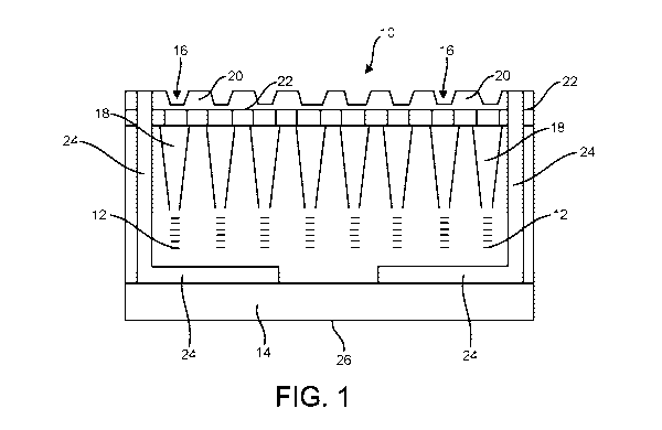
[0072] FIG. 1 illustrates one example of a light detection device 10 that may
be utilized in the
flow cells of the present disclosure. The light detection device 10 may
comprise a plurality of
stacked layers, such as a base layer or wafer 14 and a plurality of dielectric
layers and metal-
dielectric layers extending thereover. As shown in FIG. 1, the light detection
device 10 includes
a sensor array of light sensors 12 and a guide array of light guides 18. The
light detection device
may also include a reaction structure 20 extending along a top portion 22 of
the light
detection device 10, including over openings of the light guides 18. The light
detection device
10 may be configured such that each light sensor 12 corresponds or aligns with
a single light
guide 18 and/or a single reaction recess 16 (e.g., nanowell) of a reaction
structure 20 positioned
over a top surface 22 of the light detection device 10, such that it receives
photons only
therefrom. However, in other examples, a single light sensor 12 may receive
photons through
more than one light guide 18 and/or from more than one reaction recess 16. A
single light sensor
12 may thereby form one pixel or more than one pixel. As shown in FIG. 1, the
reaction recesses
16 may be defined by, for example, an indent or change in depth (or thickness)
in the top surface
of the reaction structure 20.
[0073] As shown in FIG. 1, the array of light guides 18 and reaction recesses
16 of the reaction
structure 20 (and potentially light sensors 12) may be provided in a defined
repeating pattern
such that at least some of the recesses 16 and/or light guides 18 (and
potentially light sensors 12)
are equally spaced from one another in a defined positional pattern. In other
examples, the
reaction recesses 16 and/or light guides 18 (and potentially light sensors 12)
may be provided in
a random pattern, and/or at least some of the reaction recesses 16 and/or
light guides 18 (and
potentially light sensors 12) may be variably spaced from each other. The
interstitial areas
between the array of reaction recesses 16 may be substantially flat surfaces.
As explained further
below, the array of reaction recesses 16 of the reaction structure 20 may have
at least one
corresponding reaction site provided therein (e.g., immobilized on a surface
thereof).
[0074] The area of the light detection device 10 which is light sensitive is
referred to as the
active area of the device 10. The active area of the light detection device 10
thereby includes the
area containing the light guides 18, which direct light to the light sensors
12. As noted above,
the top surface 22 of the light detection device 10 may include a reaction
structure 20 with an
16
CA 03103295 2020-12-09
WO 2020/055732 PCT/US2019/050178
array of reaction recesses 16 positioned thereover for containing at least one
corresponding
reaction site thereon/therein that are available/accessible for reagent
delivery and reaction (e.g.,
responsive to an analyte in a reaction fluid) and illumination during
operation of the flow cells.
As shown in FIG. 1, the reaction structure 20 may extend over the entirety
(e.g., at least 95%, or
at least 99%, or 100%) of the active area of the light detection device 10. In
such configurations,
the top or detector surface of the reaction structure 20 may thereby define
the active surface of
the light detection device 10 over which a reaction solution may flow and
reside and interact
with the reaction sites formed on/in the reaction recesses 16. The active
surface of the light
detection device 10 may comprise the surfaces of the recesses 16 and
interstitial areas extending
between and about the recesses 16.
100751 The exposed top surfaces of the reaction structure 20 (i.e., the
exposed top surfaces of
the reaction recesses 16 and/or the interstitial areas extending therebetween
and thereabout) may
comprise smooth planar/flat surfaces. In particular examples, the exposed top
surfaces of the
interstitial areas and/or reaction recesses 16 of the exposed top surface of
the reaction structure
20 may be smooth planar/flat surfaces that prevent reaction solution or any
other biological or
chemical substances from being trapped or remaining thereon and/or prevent pad
hopping errors.
For example, the top exposed surfaces of the reaction structure 20 may include
a surface
roughness micrometric range, such as a surface roughness of less than or equal
to 201.tm, or less
than or equal to 11.tm. In some examples, reaction structure 20 may include a
surface roughness
of less than or equal to 100nm, or less than or equal to lOnm.
[0076] The reaction structure 20 may comprise one or more layers. In one
example, the
reaction structure 20 includes a plurality of overlapping layers. The reaction
structure 20 may
include one or more layers that are configured to allow excitation light
signals and/or emitted
light signals from the reaction sites in the reaction recesses 16 (after
treatment with reaction
solution) to pass therethrough, into an opening of one or more corresponding
light guide 18, and
potentially to one or more corresponding light sensor 12 (depending upon the
configuration of
the light guides 18, for example). As another example, the reaction structure
20 may include one
more layer that prevents crosstalk or "sharing" of emitted light from a
particular reaction site in a
reaction recess 16 from propagating or passing to a non-corresponding sensor
12. The reaction
structure 20 may provide a solid surface that permits chemicals, biomolecules
or other analytes-
of-interest to be immobilized thereon. For example, each of the reaction sites
on the reaction
17
CA 03103295 2020-12-09
WO 2020/055732 PCT/US2019/050178
recesses 16 may include a cluster of biomolecules that are immobilized on the
exposed outer
surface thereof. Thus, the reaction structure 20 may comprise a material that
permits the reaction
sites to be immobilized to the reaction recesses 16. The reaction structure 20
may be physically
or chemically modified to facilitate immobilizing the biomolecules to form the
reaction sites
and/or to facilitate detection of the light emissions therefrom. Examples of
layers which may
form the reaction structure 20 include at least one SiN layer and at least one
Ta0 layer.
However, the reaction structure 20 may comprise differing layers (e.g.,
different layers, fewer
layers, and/or additional layers) and/or differing materials.
[0077] The light guides 18 may comprise a filter material configured to filter
the excitation light
or a range of wavelengths including that of the excitation light, and permit
the light
emissions from at least one reaction site of at least one corresponding
reaction recess 16 (or a
range of wavelengths including that of the light emissions) to propagate
therethrough and toward
at least one corresponding light sensor 12. The light guides 18 may be, for
example, an
absorption filter (e.g., an organic absorption filter) such that the filter
material absorbs a certain
wavelength (or range of wavelengths) and allows at least one predetermined
wavelength (or
range of wavelengths) to pass therethrough. Each of the light guides 18 of the
array may include
substantially the same filter material, or differing light guides 18 may
include differing filter
material. Each light guide 18 may thereby be configured relative to
surrounding material of the
device 10 (e.g., the dielectric material) to form a light-guiding structure.
For example, the light
guides 18 may have a refractive index of at least about 2Ø In certain
configurations, the light
guides 18 may be configured such that the optical density (OD) or absorbance
of the excitation
light is at least about 4 OD.
[0078] As shown in FIG. 1, the light detection device 10 may include circuitry
24 that transmits
or conducts signals when light emissions (e.g., photons) are detected by the
light sensors 12. As
discussed above, the light emissions may be emitted from/by the at least one
reaction site
associated with a reaction recess 16 of the reaction structure 20, and
directed or passed to an
associated light sensor 12 by at least one light guide 18. The circuitry 24
may include
interconnected conductive elements (e.g., conductors, traces, vias,
interconnects, etc.) that are
capable of conducting electrical current, such as the transmission of data
signals that are based
on detected photons. For example, the circuitry 24 may be similar to or
include a microcircuit
arrangement. The light detection device 10 may comprise at least one
integrated circuit having
18
CA 03103295 2020-12-09
WO 2020/055732 PCT/US2019/050178
an array of the light sensors 12 electrically coupled to the circuitry 24. The
circuitry 24 within
the light detection device 10 may be configured for at least one of signal
amplification,
digitization, storage, and processing. The circuitry 24 may collect (and
potentially analyze) the
light emissions detected by the sensors 12 and generate data signals for
communicating detection
data to a bioassay system. The circuitry 24 may also perform additional analog
and/or digital
signal processing in the light detection device 10.
[0079] As shown in FIG. 1, the device circuity 24 of the light detection
device 10 may extend
adjacent to, or only potentially partially through, the base portion 14. The
base portion 14 may
thereby be cavity of an electrically conductive via or other portion of the
device circuity 24 that
extends therethrough. The back side 26 of the base portion 14, which may form
an exposed back
side surface 26 of the light detection device 10, may be cavity of the device
circuity 24. Stated
differently, the device circuity 24 may be positioned fully above the back
side 26 of the base
portion 14 within the light detection device 10 such that the device circuity
24 is inaccessible at
the back side 26 of the base portion 14 and/or the device 10 itself. However,
as shown in FIG. 1,
the device circuity 24 may extend to a top side of the light detection device
10. For example, the
device circuity 24 may extend through the light detection device 10 to, and
potentially through,
the reaction structure 20. The top side of the light detection device 10,
which may be formed by
the exposed top surface of the reaction structure 20 (if present), may thereby
include the device
circuity 24, as shown in FIG. 1. Stated differently, the device circuity 24
may be exposed and
accessible at a top side of the light detection device 10, which may be a top
side surface of the
reaction structure 20 (if present), as shown in FIG. 1.
[0080] The light detection device may be manufactured using integrated circuit
manufacturing
processes, such as processes used to manufacture charged-coupled devices
circuits (CCD) or
complementary-metal-oxide semiconductor (CMOS) devices or circuits. The light
detection
device may thereby include, for example, one or more semiconductor materials,
and may take
the form of, for example, a CMOS light detection device (e.g., a CMOS image
sensor) or a CCD
image sensor, another type of image sensor. In the present example, the light
detection device 10
is a CMOS type image sensor as shown in FIG. 1, but other types of sensors may
be used. For
example, as shown in FIG. 1, the light detection device 10 may be
semiconductor based, and
comprise a plurality of stacked layers including the device base portion 14,
which may be a
silicon layer or wafer for example.
19
CA 03103295 2020-12-09
WO 2020/055732 PCT/US2019/050178
[0081] When configured as a CMOS-type light detection device 10, the
"complementary"
aspect refers to the inclusion of both n-type and p-type metal-oxide
semiconductor field effect
transistors (MOSFETs) in integrated circuits (ICs) fabricated using CMOS
technology. Each
MOSFET has a metal gate with a gate dielectric, such as an oxide (hence, the
"Metal-Oxide" part
of the name) and a semiconductor material below the gate (corresponds to
"Semiconductor" in
the name). When the light detection device 10 is configured as shown in FIG.
1, the light
sensors 12 may be electrically coupled to the circuitry 24 through the gates,
for example.
[0082] As a semiconductor based light detection device 10, at least some of
the circuitry 24
may be provided within device or substrate layers, through/into which the
lights guides 118 may
each extend. Each of the substrate layers may include interconnected
conductive elements that
forms at least part of the device circuitry 24, with dielectric material
surrounding or adjacent to
the conductive elements of the circuitry. The conductive elements of the
circuitry 24 may
thereby be embedded within dielectric material. The lights guides 18 may also
extend through
the dielectric material and may be spaced from the circuitry. Various metallic
elements and/or
dielectric materials may be used, such as those suitable for integrated
circuit manufacturing (e.g.,
CMOS manufacturing). For example, the conductive elements/circuity 24 may be
metallic
elements, such as W (tungsten) elements, Cu (copper) elements, Al (aluminum)
elements, or a
combination thereof, but it is understood that other materials and
configurations may be used.
The dielectric material may be a low-k material and/or a silicon-containing
material, such as
5i02, but it is understood that other dielectric materials and configurations
may be used.
[0083] The light detection device 10 may be an integrated circuit die. For
example, the light
detection device 10 may be manufactured as part of a large batch of a
plurality of light detection
devices 10 provided on a single base portion (e.g., a wafer) of electronic-
grade silicon (EGS) or
other semiconductor (such as GaAs). The plurality of as-manufactured devices
are thereby
integral and formed/arranged adjacent and positioned very close to each other.
The wafer is cut
(i.e., diced) into many pieces, each containing at least one distinct light
detection device 10. As
shown in FIG. 1, a single distinct light detection device 10 may be formed
(i.e., diced) from the
plurality of integral as-manufactured devices of the wafer. Alternatively, a
plurality of integral
adjacent light detection devices 10 may be formed (i.e., diced) from the
plurality of integral as-
manufactured devices of the wafer.
CA 03103295 2020-12-09
WO 2020/055732 PCT/US2019/050178
[0084] FIG. 1 illustrates another example of a light detection device 110 that
may be utilized in
the flow cells of the present disclosure. Light detection device 110 of FIG. 2
is similar to light
detection device 10 of FIG. 1, and therefore like reference numerals preceded
with "1" are used
to indicate like components, aspects, functions, processes or functions, and
the description above
directed to thereto equally applies, and is not repeated for brevity and
clarity purposes. As
shown in FIG. 2, light detection device 110 differs from light detection
device 10 in that light
detection device 110 does not include a reaction structure (forming reaction
recesses and
interstitial areas extending therebetween and thereabout) positioned over the
top surface 122
thereof Rather, the as-manufactured or diced light detection device 110 may
not include a
reaction structure. A reaction structure may be positioned on the top surface
122 of the diced
light detection device 110, such as after processing of the light detection
device 110 as explained
further below.
100851 Light detection device 110 also differs from light detection device 10
in that the circuitry
124 includes vias 128 that extend entirely through the base wafer portion 114,
as shown in FIG.
2. The vias 128 are thereby exposed and accessible at the back side 126 of the
base wafer
portion 114 and the device 110 itself As also shown in FIG. 2, the back side
126 of the base
wafer portion 114 (and the device 110 itself) includes one or more spacer
portions 130 extending
from the back side 126 of the base wafer portion 114. The at least one spacer
portion 130 may
be spaced from, positioned adjacent to, or only partially overlap the vias 128
on the back side
126 of the base wafer portion 114. In this way, the at least one spacer
portion 130 may be
positioned on the back side 126 of the base wafer portion 114 such that at
least a portion of each
via 128 is exposed and available at the back side 126 of the base wafer
portion 114 and the
device 110 itself. As shown in FIG. 2, the light detection device 110 may
include at least two
spacer portions 130 extending along opposing lateral sides of the back side
126 of the base wafer
portion 114. The at least one spacer portion 130 may provide structural
support or rigidly to the
base wafer portions 114, and thereby the device 10 itself (which may have been
compromised or
weakened by the vias 128). In some light detection devices 110, the at least
one spacer portion
130 may be electrically insulative or non-conductive (or a semiconductor) so
as to not interfere
with the operation of the sensors 112 and/or circuitry 124, for example.
Example materials
forming the at least one spacer portion 130 include, but are not limited to,
glass, fused silica,
21
CA 03103295 2020-12-09
WO 2020/055732 PCT/US2019/050178
quartz, silicon, fiberglass, plastic, epoxy, ceramic, a dielectric composite
material, paper or a
combination thereof.
[0086] As shown in FIGS. 3-5, a support structure 32 including a support frame
34 and a
support substrate 44 may be utilized to form a flow cell of the present
disclosure. The support
frame 34 may define a top surface 36, a bottom surface 38, and at least one
cavity 40 (e.g., a void
or aperture) extending through the frame 34 between the top and bottom
surfaces 36, 38. The
support structure 32 may include any number of cavities 44. As shown in FIGS.
3 and 4, the
support frame 34 may include an array of a plurality of distinct spaced
cavities 40. The array of
cavities 40 may be spaced from each other such that a portion of the support
frame 34 extends
entirely about each cavity 40, and thereby between adjacent cavities 40. The
array of cavities 40
may be defined in a repeating (potentially uniform) pattern such that the
cavities 40 are evenly or
consistently spaced apart. Alternatively, the array of cavities 40 may be
randomly distributed
such that at least some of the cavities 40 are unevenly spaced apart. As shown
in FIG. 5, each
cavity 40 may be formed by inner side walls 50 of the support frame 34 that
extend between the
top and bottom surfaces 36, 38. In some configurations, the inner side walls
50 of the support
frame 34 defining the cavities 40 may extend perpendicularly between the top
and bottom
surfaces 36, 38 such that the size of the cavities 40 may define the same size
or shape at the top
surface 36 and the bottom surface 38.
[0087] Each cavity 40 may be sized and shape to include one or more light
detection device,
such as the light detection device 110 of FIG. 2 described above as shown in
FIGS. 4 and 5.
However, as explained further below, one or more light detection devices of a
differing
configuration may be utilized within the cavities 40 of the support frame 34,
such as, but not
limited to, light detection device 10 of FIG. 1 described above. Further, at
least one light
detection device of a first configuration may be utilized with one or more
first cavities 40 of the
support frame 34, and at least one light detection device of a second
configuration may be
utilized with one or more second cavities 40 of the support frame 34.
[0088] The support frame 34 may substantially planar. For example, the top
surface 36 and/or
the bottom surface 38 of the support frame 34 may be planar and parallel. In
some
configurations, the top surface 36 and/or the bottom surface 38 may
substantially smooth, such
as including a submicron-scale surface roughness. In some configurations, the
top surface 36
and/or the bottom surface 38 may include a surface roughness of less than or
equal to 50nm or
22
CA 03103295 2020-12-09
WO 2020/055732 PCT/US2019/050178
less than or equal to lOnm. In some examples, the top surface 36 and/or bottom
surface 38 may
include a surface roughness of within the range of 1-2nm. As explained further
below, the top
surface 36 of the support frame 34 may cooperate with the detector surface of
a reaction structure
of a light detection device (e.g., the active surface of the device) to form a
flow path of the flow
cell for the delivery of the reagent solution, or a reaction structure, one or
more other layers,
and/or a lid may be positioned over the top surface 36 of the support frame 34
and the top
portion 122 of the light detection device. As such, the flatness/smoothness of
the top surface 36
of the support frame 34 (and the top surface of the reaction structure) may be
configured to
enable reagent fluidic flow without entrainment or entrapment of the fluid(s).
[0089] The support frame 34, and potentially the substrate 44, may be
relatively rigid so as to
securely hold and couple with the light detection devices 110 within the
cavities 40 and prevent
damaging distortion/deformation of the light detection devices 110 during
manufacturing,
handling and/or use of the flow cells of the present disclosure. In some
configurations, the
support frame 34 (and potentially the substrate 44) includes a young's modulus
of at least
50GPa, or at least 70GPA. In some configurations, the support frame 34 (and
potentially the
substrate 44) includes a coefficient of thermal expansion (CTE) of at least
about 20 per degree
Celsius, or at least about 30 per degree Celsius. For example, the support
frame 34 may
comprise a boro-aluminosilicate glass (e.g., Corning Eagle XG glass)
including a young's
modulus of within the range of 70-80 GPa and a CTE within the range of 30-35
per degree
Celsius, or comprised of silicon including a young's modulus within the range
of 160-170 GPa
and a CTE within the range of 35-40 per degree Celsius.
[0090] The support frame 34 may come into contact with the reagent solution
and/or other
material/solutions during formation of the reaction sites on the reaction
structure positioned over
the top portion 122 of the light detection device 110, during
illumination/detection and/or
preparation and/or cleaning of the flow cells of the present disclosure. The
support frame 34
may comprise one or more materials that are unreactive to sequencing reagents,
such as a
sequencing reagent utilized for DNA grafting, clustering, cleaving,
incorporating and/or reading.
For example, a sequencing solution may be an aqueous solution and/or may be
comprised of an
oil.
[0091] The support frame 34 may be subject to a chemical mechanical polishing
(CMP) process
during the formation of one or more flow cells therefrom, as explained further
below. The
23
CA 03103295 2020-12-09
WO 2020/055732 PCT/US2019/050178
support frame 34 may comprise one or more materials that are unreactive to CMP
slurries and
mixtures that come into contact with the support frame 34 during the formation
of one or more
flow cells therefrom. For example, a CMP slurry or mixture may comprise
abrasive particles
and a base liquid. In some examples, the base liquid may comprise water (e.g.,
deionized water)
and/or an oil. In some examples, the abrasive particles may comprise an oxide,
such as silicon
dioxide, cerium oxide and/or aluminum oxide, for example.
[0092] The support frame 34 may electrically insulate the at least one light
detection device 110
positioned within each cavity 40, such as to not interfere with the light
sensing operation thereof
At least a portion of the thickness/cross-section of portions of the support
frame 34
surrounding/forming the cavities 40 (extending between the top and bottom
surfaces 36, 38) may
comprise an electrically insulative (i.e., non-conductive) material (or a
semiconductor material).
For example, at least a portion of the thickness/cross-section of portions of
the support frame 34
surrounding/forming the cavities 40 extending from the top surface 36, or a
medial portion
spaced between the top and bottom surfaces 36, 38, may comprise an
electrically insulative (i.e.,
electrically non-conductive) material (or semiconductor material). In some
configurations, the
support frame 34 may comprise only the electrically insulative material.
Example electrically
insulative materials that may form at least a portion of the support frame
include silicon, glass
(e.g., quartz, fused silica, fiberglass, borosilicate glass (e.g., alkaline
earth boro-aluminosilicate
glass, such as Corning Eagle XG glass), floated borosilicate glass (e.g.,
Borofloat 33 glass),
or other low autofluorescence glasses), ceramic, polymers (e.g., plastic,
epoxy, silicon charged
epoxy or UV curable epoxy or adhesives), dielectric composite materials, paper
or a combination
thereof
[0093] However, as explained further below, portions of the support frame 34
may comprise an
electrically conductive material, such as a metal material. For example, as
explained further
below, the support frame 34 may include electrically conductive vias extending
through the
thickness/cross-section of portions of the support frame 34 proximate to
(e.g., adjacent to) the
cavities 40 extending between the top and bottom surfaces 36, 38 (and exposed
at the top and
bottom surfaces 36, 38). In some configurations, a portion of the
thickness/cross-section of
portions of the support frame 34 surrounding/forming the cavities 40 extending
from the top
surface 36 and/or the bottom surface 34 may comprise an electrically
conductive material (which
may comprise a portion of the vias).
24
CA 03103295 2020-12-09
WO 2020/055732 PCT/US2019/050178
[0094] The support frame 34 may include a plurality of visual
indications/markings 45, as
shown in FIG. 4. The visual indications 45 can be utilized to reference the
position and/or
orientation of the support frame 34 as a whole and/or portions thereof or
components coupled
thereto (such as the cavities 40 and one or more light detection device 110
positioned within the
cavities 40, as explained further below, for example). In this way, the visual
indications 45 can
be utilized as alignment marks during processing of the support frame 34 (and
components
coupled thereto, as explained further below) into one or more intermediate
flow cell devices
and/or flow cell devices (as explained further below). For example, the visual
indications 45
may be utilized for alignment during lidding and/or dicing operations to form
one or more
intermediate flow cell devices and/or flow cell devices.
[0095] The visual indications 45 may comprise any material that visually
differs from the
support frame 34, such as with respect to a human eye and/or an imaging device
(e.g., a digital
camera). In some examples, the visual indications 45 may comprise a pigment,
paint, dye,
luminescent material, metal, oxide or a combination thereof. The visual
indications 45 may
comprise one or more materials that are unreactive to sequencing reagents
and/or CM' slurries.
[0096] The visual indications 45 may be provided on the bottom surface 38 (as
shown in FIG.
4) of the support frame 34, on the top surface 36 of the support frame 34,
embedded at least
partially within the thickness of the support frame 34 between the top and
bottom surfaces 36, 38
of the support frame 34, or a combination thereof. The visual indications 45
may be formed on
the support frame 34 via any process. In some examples, the visual indications
45 may formed
on the support frame 34 via a printing process, such as a spraying process or
a lithography
process.
[0097] As shown in FIGS. 4 and 5, the support structure 32 may include the top
surface 36 of
the support frame 34 coupled to the top surface 46 of the substrate or carrier
44. The support
frame 34 and the substrate 44 may be removably coupled or fixedly coupled. In
some support
structures 32, the substrate 44 may be comprised of the same or similar
material as the material
of the support frame 34. In some other support structures 32, the substrate 44
may be comprised
of a differing material than the material as the support frame 34. The top
surface 46 of the
substrate 44 may be substantially smooth and planar such that the top surface
36 of the support
frame 34 and the top surface 46 of the substrate 44 are parallel, and
potentially substantially
CA 03103295 2020-12-09
WO 2020/055732 PCT/US2019/050178
coplanar as shown in FIG. 5. In some configurations, the top surface 46 of the
substrate 44 may
define the same or similar surface smoothness as the top surface 36 of the
support frame 34.
[0098] As also shown in FIGS. 4 and 5, with the top surface 36 of the support
frame 34 coupled
to the top surface 46 of the substrate 44, the at least one diced light
detection device 110 may be
positioned within a cavity 40 "facedown" such that the top surface 122 of the
at least one light
detection device 110 is positioned on or adjacent to the top surface 46 of the
substrate 44. In this
way, the top surface 122 of the at least one light detection device may be
substantially aligned
(e.g., co-planar) with the top surface 36 of the support frame 34. Similarly,
if the at least one
diced light detection device 110 includes a reaction structure provided over
the top surface 122
(e.g., as with light detection device 10 of FIG. 1), the top surface of the
detector/active surface of
the reaction structure may be positioned on or adjacent to the top surface 46
of the substrate 44
and the interstitial portions may be substantially aligned (e.g., co-planar)
with the top surface 36
of the support frame 34.
[0099] As shown in FIG. 5, the support frame 34 may be thinner than the at
least one light
detection device 110 such that the back side 126 thereof extends past the
bottom surface 38
support frame 34. In some other support frame 34 configurations, the bottom
surface 38 support
frame 34 may be even with or below the back side 126 of the at least one light
detection device
110. The at least one light detection device 110 may define a smaller
corresponding size than the
cavity 40. The diced at least one light detection device 110 may thereby be
positioned within a
cavity 40 of the support structure 32 such that the periphery of the at least
one light detection
device 110 is spaced from the inner side walls 50 of the support frame 34, as
shown in FIG. 5.
For example, a portion of the cavity 40 may extend about the periphery of the
at least one light
detection device 110 to form a trench or edge cavity portion 52 that extends
between the inner
side walls 50 of the cavity 40 of the support frame 34 and the periphery of
the at least one light
detection device 110.
[0100] The at least one light detection device 110 may freely lie directly on
the top surface 46
of the substrate 44 in the cavity 40. In some such arrangements, the at least
one light detection
device 110 may be mechanically held in the cavity 40 via a tool or support
member.
[0101] Another example of a support structure 232 according to the present
disclosure is shown
in FIG. 6. Support structure 232 of FIG. 6 is similar to support structure 32
of FIGS. 3-5, and
therefore like reference numerals preceded with "2" are used to indicate like
components,
26
CA 03103295 2020-12-09
WO 2020/055732 PCT/US2019/050178
aspects, functions, processes or functions, and the description above directed
to thereto equally
applies, and is not repeated for brevity and clarity purposes. As shown in
FIG. 6, the support
structure 232 differs from support structure 32 with the inclusion of an
interposer member or
layer 248 that chemically couples/bonds the top portion 122 of the at least
one light detection
device 210 to the top surface 246 of the substrate 244 within the cavity 244.
The interposer layer
248 may be any temporary or removable bonding material (e.g., via one or more
chemical,
mechanical and/or irradiation process). In one example, the interposer layer
248 may comprise a
polymer material (e.g., one or more cyclic olefin copolymer), which may be
provided within a
solvent-cast bonding material composition. For example, the interposer layer
248 may comprise
a BrewerBond temporary bonding material sold by Brewer Science, Inc., such as
BrewerBond 220 or BrewerBond 305. In another example, the interposer layer
248 may
comprise a high UV absorbance release layer and/or an adhesive layer, such as
a JSR ELPAC
TA series temporary bonding material sold by the JSR Corporation. The
interposer layer 248
may be formed by spin coating, spray coating, dye slot coating or lamination,
for example, onto
the top surface 246 of the substrate 244.
[0102] The interposer layer 248 may comprise one or more layers of material
that extends over
the top surface 246 of the substrate 244 within the cavity 240. The top
portion 122 of the at least
one light detection device 110 may thereby lie on a top surface 247 of the
interposer layer 248
within the cavity 244. The interposer layer 248 may also extend between the
top surface 246 of
the substrate 244 and the top surface 236 of the support frame 234, as shown
in FIG. 6. The top
side 236 of the support frame may thereby extend over the top surface 247 of
the interposer layer
248, and the interposer layer 248 may extend over the top side 246 of the
substrate 244.
[0103] Another example of a support structure 332 according to the present
disclosure is shown
in FIG. 7. Support structure 332 of FIG. 7 is similar to support structure 32
of FIGS. 3-5 and
support structure 232 of FIG. 6, and therefore like reference numerals
preceded with "3" are used
to indicate like components, aspects, functions, processes or functions, and
the description above
directed to thereto equally applies, and is not repeated for brevity and
clarity purposes. As
shown in FIG. 7, the support structure 332 differs from support structure 32
and support structure
232 with the inclusion of a spacer member/layer 349 that spaces the top
surface 346 of the
substrate 344 from the top portion 122 of the at least one light detection
device 110. The spacer
layer 349 may only extend between top surface 346 of the substrate 344 and the
top surface 336
27
CA 03103295 2020-12-09
WO 2020/055732 PCT/US2019/050178
of the support frame 334, and thereby not extend through the cavity 340. In
this way, the spacer
layer 349 raises the top surface 336 of the support frame 334 from the top
surface 346 of the
substrate 344, on which the top portion 122 of the at least one light
detection device 110 overlies.
In this way, the spacer layer 349 spaces the top portion 122 of the at least
one light detection
device 110 past (i.e., above) the top surface 336 of the support frame 334 in
a direction extending
from the back side 126 to the top portion 122 of the at least one light
detection device 110. The
spacer layer 349 may comprise the same or similar material as the interposer
layer 248. The
spacer layer 349 may be formed by spin coating, spray coating, dye slot
coating or lamination,
for example, onto the top surface 346 of the substrate 344. Although the
support structure 332 of
FIG. 7 is shown as not including an interposer layer (e.g., the interposer
layer 248 of the support
structure 232 of FIG. 6), the support structure 332 may include an interposer
extending over the
top surface 336 of the substrate 344 between the substrate 344 and the support
frame 334 and
across the cavity 340.
[0104] Another example of a support structure 432 according to the present
disclosure is shown
in FIG. 8. Support structure 432 of FIG. 8 is similar to support structure 32
of FIGS. 3-5,
support structure 232 of FIG. 6 and support structure 332 of FIG. 7, and
therefore like reference
numerals preceded with "4" are used to indicate like components, aspects,
functions, processes
or functions, and the description above directed to thereto equally applies,
and is not repeated for
brevity and clarity purposes. As shown in FIG. 8, the support structure 432
differs from support
structure 32, the support structure 232 and the support structure 332 in the
configuration of the
side walls 450 of the cavities 440.
[0105] As shown in FIG. 8, each cavity 440 may be formed by inner side walls
450 of the
support frame 434 that extend between the top and bottom surfaces 436, 438.
The inner side
walls 450 of the support frame 434 defining the cavities 440 may extend
inwardly toward the
interior of the cavities 440 as they extend from the bottom surface 438 to the
top surface 436
such that the size of the cavities 440 is smaller or narrower at the top
surface 436 as compared to
the bottom surface 438 (i.e., the opening of each cavity 440 at the bottom
surface 438 is larger
than the opening thereto at the top surface 436). It is noted that the side
walls 450 may extend
very close to, but still be spaced from, the periphery of the at least one
light detection device 110
at the top surface 436. Correspondingly, the edge cavity portion 452 of the
cavity 440 that
28
CA 03103295 2020-12-09
WO 2020/055732 PCT/US2019/050178
extends between the inner side walls 450 and the periphery of the at least one
light detection
device 110 may narrow as it extends from the bottom surface 438 to the top
surface 436.
[0106] The shape or configuration of the inner side walls 450 may be formed by
any
configuration of the support frame 434 and/or manufacturing or processing
technique. For
example, the support frame 434 may comprise a plurality of support frame
layers with differing
sized openings such that when stack together, the openings form the cavities
40. As another
example, the shape or configuration of the inner side walls 450 may be formed
by etching or
otherwise shaping or forming the support frame 434.
[0107] In one example, the inner side walls 450 may extend linearly on an
angle from the top
surface 436 to the bottom surface 434 (i.e., are planar) inwardly toward the
interior of the
cavities 440, as shown in FIG. 8. In other examples, the inner side walls 450
may not extend
linearly (i.e., planar). For example, the inner side walls 450 may extend
rectilinearly,
curvilinearly or a combination thereof from the bottom surface 438 to the top
surface 436 such
that the size of the cavities 440 is smaller or narrower at the top surface
436 as compared to the
bottom surface 438. In one such example, a portion of the inner side walls 450
of the support
frame 434 defining the cavities 440 may extend perpendicularly from the bottom
surface 438
toward the top surface 436 along a portion of the thickness of the support
frame 534, and another
portion may extend linearly at an angle (i.e., angles planes) inwardly toward
the interior of the
cavities 540 therefrom to the top surface 436.
[0108] FIGS. 9-11B illustrates coupling a single distinct light detection
device 110 within each
cavity 40 of the support frame 34 of the support structure 32 of FIGS. 3-5 via
support/filler
material 60. As shown in FIG. 9, the support material 60 may be introduced
into the edge cavity
portion 52 between the side walls 50 of the support frame 34 and the periphery
of the light
detection device 110 from the exposed side thereof adjacent the bottom surface
38 of the support
frame 34. The support material 60 may securely couple the support frame 34 and
the light
detection device 110 together. Specifically, as shown in FIGS. 11A and 11B,
the support
material 60 may extend about the periphery of the lateral sides of the of the
light detection device
110 positioned within the cavity 40. The support material 60 may thereby
extend between, and
couple together, the periphery of the lateral sides of the of the light
detection device 110
positioned within the cavity 40 and the side walls 50 of the cavity 40. In
some examples, after
the support material 60 is deposited within each cavity 40, the bottom surface
38 of the support
29
CA 03103295 2020-12-09
WO 2020/055732 PCT/US2019/050178
frame 34, the support material 60 and/or the light detection device(s) 110
within each cavity 40
may be subjected to one or more CM' operations. For example, the support
material 60 and/or
the light detection device(s) 110 within at least one cavity 40 may extend
higher than (i.e.,
above) at least a proximate portion of the bottom surface 38 of the support
frame 34, and the one
or more CM' operations may remove a portion of the support material 60 and/or
the light
detection device(s) 110 to planarize the bottom surface 38 of the support
frame 34, the support
material 60 and the light detection device(s) 110.
[0109] The support material 60 may be any material that is able to flow into
or otherwise be
introduced into the edge cavity portions 52 (such as in a first state, e.g., a
liquid or powdered
state), and securely couple the support frame 34 and the light detection
devices 110 within the
cavities 40 together (such as in a second state, e.g., a hardened or cured
state). The support
material 60 may be electrically insulative or non-conductive (or a
semiconductor) so as to not
interfere with the operation of the light detection devices 110 (e.g., the
operation of the sensors
112 and/or circuitry 124). The support material 60 may come into contact with
the reagent
solution and/or other material/solutions during formation of the reaction
structure, formation of
the reaction sites on the reaction structure, illumination/detection and/or
preparation and/or
cleaning of the flow cells of the present disclosure. As such, the support
material 60 may
comprise one or more materials that are unreactive to sequencing reagents,
such as a sequencing
reagent utilized for DNA grafting, clustering, cleaving, incorporating and/or
reading. For
example, a sequencing reagent may include water and/or an oil. Example
materials of the
support material 60 include silicon, glass (e.g., quartz, fused silica,
fiberglass, borosilicate glass
(e.g., alkaline earth boro-aluminosilicate glass, such as Corning Eagle XG
glass), floated
borosilicate glass (e.g., Borofloat 33 glass), or other low autofluorescence
glasses), ceramics,
polymers (e.g., plastic, epoxy, silicon charged epoxy or UV curable epoxy or
adhesives),
dielectric composite materials or a combination thereof
[0110] As shown in FIGS. 10-11B, after the support material 60 fills the edge
cavity portion 52
and fixedly couples the support frame 34 and the at least one light detection
device 110 with at
least one cavity 40, the remainder of the support structure 32 may be removed
therefrom. For
example, the substrate 44, and any interposer and/or spacer layers/members
associated therewith,
may be removed from the top surface 36 of the support frame 34, the top
portion 122 of the light
detection device 110, and a top surface of the support material 60, as shown
in FIG. 10. The
CA 03103295 2020-12-09
WO 2020/055732 PCT/US2019/050178
isolated support frame 34, at least one light detection device 110 positioned
within at least one
cavity 40, and the deposited support material 60 may comprise an intermediate
flow cell device
62, as shown in FIGS. 11A and 11B. The intermediate flow cell device 62 can be
further
processed into one or more flow cells, as explained further below. As noted
above, although the
light detection devices 110 of FIG. 2 are illustrated in the array of cavities
40 of the support
frame 34 of the intermediate flow cell device 62 of FIGS. 9-11B, light
detection devices of other
configurations, such as the light detection device 10 of FIG. 1, may similarly
or equally be
utilized within at least one cavity 40 of the support frame 34.
[0111] The mode or method of removal of the intermediate flow cell device 62
from the other
portion(s) of the support structure 32 may be related to, at least in part,
the material of the
support frame 34 and the substrate 44 (and/or any interposer and/or spacer
layers/members
associated therewith) and/or the mode of attachment of thereof In some
configurations, the
intermediate flow cell device 62 may be de-bonded from the remainder of the
support structure
32. In some configurations, the substrate 44, and any interposer and/or spacer
layers/members
associated therewith if present, may be chemically and/or mechanically etched
from the
intermediate flow cell device 62. In some configurations, the substrate 44,
and any interposer
and/or spacer layers/members associated therewith if present, may be removed
from the
intermediate flow cell device 62 via air blowing, blade insertion, vacuum
debonding or
mechanical lifting with or without pre-processing (such as edge trimming or
laser patterning), for
example.
[0112] As shown in FIGS. 9-11B, in some configurations a single distinct light
detection device
110 may be positioned within at least one cavity 40 of the support frame 34.
As described above
and as shown in FIGS. 9-11B, in such a configuration the support material 60
may be disposed
within the edge cavity portion 52 between the side walls 50 of the support
frame 34 and the
periphery of the single distinct light detection device 110 within a
respective cavity 40 to couple
the support frame 34 and the single distinct light detection device 110
together.
[0113] As shown in FIGS. 12A and 12B, in some other intermediate flow cell
device 662
configurations a plurality of spaced distinct light detection devices 110A,
110B, 110C may be
positioned within at least one cavity 640 of a support frame 634. It is noted
that although three
light detection devices 110A, 110B, 110C are used herein to illustrate
utilization of a plurality of
light detection devices, any number of light detection devices may equally be
employed (e.g.,
31
CA 03103295 2020-12-09
WO 2020/055732 PCT/US2019/050178
two light detection devices, three light detection devices, four light
detection devices, five light
detection devices, etc.). Intermediate flow cell device 662 of FIGS. 12A and
12B is similar to
intermediate flow cell device 62 of FIGS. 11A and 11B, and therefore like
reference numerals
preceded with "6" as opposed to "1" are used to indicate like components,
aspects, functions,
processes or functions, and the description above directed to thereto equally
applies, and is not
repeated for brevity and clarity purposes.
[0114] As shown in FIG. 12A and 12B, in such a configuration of the
intermediate flow cell
device 662 the support material 660 may be disposed within the edge cavity
portion 652 between
the side walls 650 of the support frame 634 and the peripheral sides of the
plurality of spaced
distinct light detection devices 110A, 110B, 110C adjacent and/or facing
thereto to couple the
support frame 634 and the light detection devices 110A, 110B, 110C together.
Further, as shown
in FIGS. 12A and 12B, the distinct light detection devices 110A, 110B, 110C
may be spaced
from each other such that an interstitial or inter-device portion 653 of the
cavity 640 is positioned
between adjacent distinct light detection devices 110A, 110B, 110C. The
support material 660
may be disposed within the interstice portion 652 between adjacent distinct
light detection
devices 110A, 110B, 110C to couple the devices 110A, 110B, 110C together and
to the support
frame 634. In this way, the support material 660 may extend about the
periphery of the spaced
distinct light detection devices 110A, 110B, 110C positioned within the cavity
640.
[0115] As shown in FIGS. 13A and 13B, in some other intermediate flow cell
device 762
configurations a plurality of integral, coupled or non-spaced distinct light
detection devices
110A, 110B, 110C may be positioned within at least one cavity 740 of a support
frame 734.
Intermediate flow cell device 762 of FIGS. 13A and 13B is similar to
intermediate flow cell
device 62 of FIGS. 11A and 11B and intermediate flow cell device 662 of FIGS.
12A and 12B,
and therefore like reference numerals preceded with "7" as opposed to "1" or
"6," respectively,
are used to indicate like components, aspects, functions, processes or
functions, and the
description above directed to thereto equally applies, and is not repeated for
brevity and clarity
purposes.
[0116] As shown in FIG. 13A and 13B, in such a configuration of the
intermediate flow cell
device 762 the support material 760 may be disposed within the edge cavity
portion 752 between
the side walls 750 of the support frame 734 and the exposed peripheral sides
of the plurality of
integral, coupled or non-spaced distinct light detection devices 110A, 110B,
110C adjacent
32
CA 03103295 2020-12-09
WO 2020/055732 PCT/US2019/050178
and/or facing thereto to couple the support frame 734 and the light detection
devices 110A,
110B, 110C together. As the plurality of light detection devices 110A, 110B,
110C are integral,
coupled or non-spaced, the cavity 740 does not extend between adjacent devices
110A, 110B,
110C (and therefore the support material 760 does not extend between adjacent
devices 110A,
110B, 110C). As discussed above, the plurality of distinct light detection
devices 110A, 110B,
110C may be manufactured as a portion of a wafer of a plurality of integral or
coupled distinct
light detection devices 110A, 110B, 110C. The wafer of devices may be diced
into single
distinct light detection devices (as shown in FIGS. 10-12B) and/or a plurality
of integral or
coupled distinct light detection devices (comprised of any number of
individual distinct devices)
(as shown in FIGS. 13A and 13B).
[0117] FIG. 14 illustrates an intermediate flow cell device 862 formed via a
frame 834 and at
least one light detection device 10 within one or more cavities 840 thereof
but without a base
substrate or any associated interposer and/or spacer layers. Intermediate flow
cell device 862 of
FIG. 14 is similar to intermediate flow cell device 62 of FIGS. 11A and 11B,
intermediate flow
cell device 662 of FIGS. 12A and 12B and intermediate flow cell device 762 of
FIGS. 13A and
13B, and therefore like reference numerals preceded with "8" are used to
indicate like
components, aspects, functions, processes or functions, and the description
above directed to
thereto equally applies, and is not repeated for brevity and clarity purposes.
Although only a
single light detection device 110 is illustrated in each cavity 840 in FIGS.
15A and 15B, as
discussed above a cavity 840 may include a plurality of spaced light detection
devices 110, and
the support material 860 may extend between adjacent spaced light detection
devices 110.
Further, although the light detection devices 10 of the FIG. 1 as shown in
each cavity 840, as
discussed above other light detection devices 10 may be equally utilized, such
as the light
detection device 110 of FIG. 2.
[0118] Intermediate flow cell device 862 differs from intermediate flow cell
device 62,
intermediate flow cell device 662 and intermediate flow cell device 762 in the
configuration of
the cavities 840 of support frame 834 and support material 860. As shown in
FIG. 14, the
cavities 840 extend only partially through the thickness of the support frame
840. The cavities
840 extend from the top surface 836 and toward the bottom surface 838 of the
support frame 840
through a portion of thereof. A bottom portion 841 of the support frame 841
thereby extends
33
CA 03103295 2020-12-09
WO 2020/055732 PCT/US2019/050178
between a bottom surface 843 of the cavities 840 and the bottom surface 838 of
the support
frame 840, as shown in FIG. 14.
[0119] As also shown in FIG. 14, a bottom layer or portion 863 of the support
material 860 may
extend over the bottom surface 843 of the cavities 840, and at least one light
detection device 10
may be positioned thereon. In this way, the bottom portion 863 of the support
material 860 may
extend between the bottom surface 26 of the at least one light detection
device 10 and the bottom
surface 843 of the respective cavity 840.
[0120] In some examples, the support material 860 may initially be provided
over the bottom
surface 843 of the cavities 840 to form the bottom portion 863 thereof, and at
least one light
detection device 10 placed thereon such that the bottom portion 863 of the
support material 860
couples or otherwise holds the at least one light detection device 10 in place
within the respective
cavity 840 for further processing. For example, after placement of at least
one light detection
device 10 over/on the bottom portion 863 of the support material 860 (e.g.,
the bottom surface 26
of the of at least one light detection device 10 positioned on an exposed top
surface of the bottom
portion 863 of the support material 860), additional support material 860 may
be introduced into
the edge cavity portion 852 between the side walls 850 of the support frame
834 and the
periphery of the at least one light detection device 10 and over the exposed
portions of the
(previously-formed) bottom portion 863 of the support material 860. In some
other examples,
the bottom portion 863 of the support material 860 may not be present, and at
least one light
detection device 10 may be positioned directly on the bottom surface 838 of
the support frame
840 (or another layer or material may be positioned therebetween).
[0121] As shown in FIGS. 15A and 15B, after formation of an intermediate flow
cell device
962, a top surface 961 of the support material 960 within the cavities 940 may
be exposed.
Intermediate flow cell device 962 of FIGS. 15A and 15B is similar to
intermediate flow cell
device 62 of FIGS. 11A and 11B, intermediate flow cell device 662 of FIGS. 12A
and 12B,
intermediate flow cell device 762 of FIGS. 13A and 13B and intermediate flow
cell device 862
of FIG. 14, and therefore like reference numerals preceded with "9" are used
to indicate like
components, aspects, functions, processes or functions, and the description
above directed to
thereto equally applies, and is not repeated for brevity and clarity purposes.
For example,
intermediate flow cell device 962 may be formed via removal or separation of a
support substrate
and any associated interposer and spacer layers from the top surface 936 of
the support frame
34
CA 03103295 2020-12-09
WO 2020/055732 PCT/US2019/050178
934, the top surface 961 of the support material 960 and the top surface 122
of the light detection
devices 110. Alternatively, the intermediate flow cell device 962 may be
formed without a
support substrate, such as if the cavities 840 extend only partially through
the support frame 834.
[0122] As shown in FIGS. 15A and 15B, at least a portion of the exposed top
surface 961 of the
support material 960 may extend below and between the top surface/side 936 of
the support
frame 931 and the adjacent top portion 122 of the at least one light detection
device 110
positioned within the respective cavity 940. Although only a single light
detection device 110 is
illustrated in FIGS. 15A and 15B, as discussed above a cavity 940 may include
a plurality of
spaced light detection devices 110, and the support material 960 may extend
between adjacent
spaced light detection devices 110. In such an example, the top surface 961 of
such portions of
the support material 960 may extend below and between the top portions 122 of
the adjacent
light detection devices 110. The top surface 961 of the support material 960
positioned
throughout a respective cavity 940 may thereby comprise a recessed top side
surface portion that
is positioned below the top side 936 of the support frame 931 and the top
portion 122 of the at
least one light detection device 110 positioned within a respective cavity
940.
[0123] In some such intermediate flow cell devices 962, the top portion 122 of
the at least one
light detection device 110 positioned within a respective cavity 940 may not
include a reaction
structure extending thereover, as shown in FIG. 15A. As shown in FIG. 15B, in
some such
intermediate flow cell devices 962 a reaction structure 120 may be positioned
over the top
portion 122 of the at least one light detection device 110 and the top side
961 of the support
material 960 within a respective cavity 940 that fills in any recessed
portions thereof to form a
planar top surface from which the plurality of nanowells 16 extend.
[0124] It is noted that the reaction structure 120 can be positioned on the
top portion 122 of the
at least one light detection device 110 over the entirety of the active area
of the at least one light
detection device 110. The planar top surface of the reaction structure 120 may
thereby comprise
the top surface of the portion of the reaction structure 120 positioned over
the support material
960 within the respective cavity 940, and the top surface of the interstitial
areas of the reaction
structure 120 may be positioned over the at least one light detection device
110 within a
respective cavity 940. The top surface of the portion of the reaction
structure 120 positioned
over the support material 960 within a respective cavity 940, and the top
surface of the interstitial
CA 03103295 2020-12-09
WO 2020/055732 PCT/US2019/050178
areas of the reaction structure 120 positioned over the at least one light
detection device 110
within a respective cavity 940, may thereby be coplanar.
[0125] As also shown in FIG. 15B, the reaction structure 120 may further
extend over the top
surface 936 of the support frame 934. The planar top surface of the reaction
structure 120 may
thereby also extend over at least the top surface 936 of the support frame 934
about a respective
cavity 940. The top surface of the portion of the reaction structure 120
positioned over the
support material 960 within a respective cavity 40, the top surface of the
portion of the reaction
structure 120 positioned over the top surface 936 of the support frame 934
about the respective
cavity 940, and the top surface of the interstitial areas of the reaction
structure 120 positioned
over the at least one light detection device 110 within the respective cavity
940, may thereby be
coplanar.
[0126] Layer-fabricating processes that may be used to form the reaction
structure 120 include
photolithography, etching (e.g., reactive-ion etching), sputtering,
evaporation, casting (e.g., spin
coating), chemical vapor deposition, electrodeposition, epitaxy, thermal
oxidation, physical
vapor deposition, and the like. In some examples, the reaction structure 120
may be formed
using a shadow technique. In some examples, the reaction structure 12 may be
formed using
nanolithography, such as nanoimprint lithography (NIL). In one example, the
reaction structure
120 may be formed, at least in part, via one or more layers of an ultraviolet
light (UV) curable
resin positioned over the top surface 936 of the support frame 934, the top
portion 122 of the at
least one light detection device 110, and the top side 961 of the support
material 960 within a
respective cavity 940 via one or more NIL-related processes.
[0127] In one example, the reaction structure 120 may comprise at least one
layer positioned
over at least the top portion 122 of the light detection device 110 that is
configured to have an
array of the reaction recesses 16 (e.g., nanowells) (as discussed above with
respect to FIG. 1). In
another example, the at least one layer of the reaction structure 120 may
include pre-formed
reaction recesses 16. Optionally, the at least one layer of the reaction
structure 120 may be
etched to remove portions thereof to form at least a portion of the reaction
recesses 16.
[0128] In one other example, the reaction structure 120 with the reaction
recesses 16 may be
formed by shaping the at least one layer of the reaction structure 120. For
example, an NIL
material may be deposited at least over the top portion 122 of the light
detection device 110. The
NIL material may comprise a material that is capable of being imprinted using
an NIL technique.
36
CA 03103295 2020-12-09
WO 2020/055732 PCT/US2019/050178
For example, the NIL material may comprise a polymer. The NIL material may
then be
imprinted or stamped with a mold (also called template) having a pattern of
features that form
the reaction recesses 16 in the NIL layer. In some configurations, the mold is
transparent to
allow UV or visible light to propagate therethrough. In such configurations,
the NIL material
may comprise a photocurable polymer that is cured by the UV or visible light
while the mold is
pressed into the NIL material. Accordingly, the NIL material may cure (e.g.,
harden) to form the
reaction recesses 16. This process may be identical or similar to step-and-
flash imprint
lithography (SFIL). In other configurations, the NIL material may be cured by
application of
thermal energy and/or pressure.
[0129] FIGS. 16A-16D illustrate an example process of forming a plurality of
backside
electrical contacts 1072 on the back side of an intermediate flow cell device
1062 that can
transmit or conduct the data signals from the circuitry 124 of the at least
one light detection
devices 110 (based on photons detected by the light sensors 116 thereof)
within a respective
cavity 1040, such as to transmit the data signals to a biosensor and/or
bioassay system when a
flow cell formed via the intermediate flow cell device 1062 is utilized
therewith. While the
intermediate flow cell device 1062 is shown with the configuration of
intermediate flow cell
device 62 of FIGS. 11A and 11B, the intermediate flow cell device 1062 may
configured
differently, such as the configurations of intermediate flow cell device 662
of FIGS. 12A and
12B or intermediate flow cell device 762 of FIGS. 13A and 13B, and therefore
like reference
numerals preceded with "10" are used to indicate like components, aspects,
functions, processes
or functions, and the description above directed to thereto equally applies,
and is not repeated for
brevity and clarity purposes. It is noted that the backside contacts 1072 on
the back side of an
intermediate flow cell device 1062 are coupled to backside vias 128 of the at
least one light
detection device 110 within a respective cavity 1040. Therefore, the while the
intermediate flow
cell device 1062 is shown utilizing light detection devices 110 of FIG. 2,
other light detection
device configurations that include backside vias 128 may be equally utilized.
[0130] As shown in FIGS. 16A and 16B, a non-electrically conductive substrate
or material
1070 is positioned on a back side of the intermediate flow cell device 1062.
As also shown in
FIGS. 16A and 16B, the back side 1074 of the substrate 1070 includes the
plurality of exposed
electrically conductive backside contacts 1072 coupled thereto. The backside
contacts 1072 may
be at least partially embedded within the back side 1074 of the substrate
1070. A backside
37
CA 03103295 2020-12-09
WO 2020/055732 PCT/US2019/050178
contact 1072 (potentially a separate and distinct backside contract 1072) may
be provided for
each backside via 128 (i.e., an exclusively associated via 128) of each light
detection device 110
within each cavity 1040. As shown in FIG. 16B, adjacent backside contacts 1072
may be spaced
from each other, and a portion of the substrate 1070 may extend therebetween.
[0131] The substrate 1070 may comprise any electrically non-conductive
material or
semiconductor material, such as a polymer (e.g., an epoxy), silicon, glass,
ceramic or a
combination thereof. The backside contacts 1072 may comprise any electrically
conductive
material, such as a metal (e.g., copper). In some examples, the substrate 1070
and the backside
contacts 1072 may comprise a printed circuit board.
[0132] As shown in FIG. 16B, the substrate 1070 and/or the backside contacts
1072 may
comprise through-holes 1076 that at least partially align (e.g., overlap) the
back side 126 of the at
least one light detection device 110 within each cavity 1040 of the support
frame 1034. The
through-holes 1076 thereby at least partially align (e.g., overlap) with the
opening/space between
the spacers 130 (if provided) and the vias 128 extending through the base
wafer portion 114 at
the back side 126 of the at least one light detection device 110 within each
cavity 1040.
[0133] As shown in FIG. 16C, an electrically conductive wires or other
structures 1080 may be
coupled between the vias 128 of the at least one light detection device 110
within each cavity
1040 and the adjacent or associated backside contacts 1072. The wires 1080 may
comprise any
electrically conductive material, such as a metal (e.g., copper). The wires
1080 can transmit the
data signals from the vias 128 of the circuitry 124 of the at least one light
detection device 110 to
the backside contacts 1072. Each wire 1080 may thereby extend from a
respective contact 1072
on the backside of the intermediate flow cell device 1062, into and through an
adjacent or
associated through-hole 1076, and to a respective via 128 of a light detection
device 110 within a
cavity 1040 of the support frame 1034, as shown in FIG. 16C. In some examples,
the wires 1080
may be spaced inwardly from the inner side walls of the through-holes 1076.
[0134] With the wires 1080 coupled between respective vias 128 and backside
contacts 1072,
the wires 1080 may be covered, enclosed/encased within insulative portions
1082, as shown in
FIG. 16D. The insulative portions 1082 may comprise an electrically insulative
material so as to
electrically insulate the wires 1080. As shown in FIG. 16D, the insulative
portions 1082 may
cover the portion (or entirety) of the back side 126 of the at least one light
detection device 110
within each cavity 1040 that is exposed to a through-hole 1076. For example,
the insulative
38
CA 03103295 2020-12-09
WO 2020/055732 PCT/US2019/050178
portion 1082 may extend over and fill the space between the spacers 130 (if
provided) of each
light detection device 110 with a respective cavity 1040.
[0135] Each insulative portion 1082 may also fill the through-hole 1076, and
extend over only a
portion of the backside contacts 1072 associated with each cavity 1040 so as
to form exposed
portions of the backside contacts 1072. For example, an insulative portion
1082 may extend
only over the portions the backside contacts 1072 that couple with respective
wires 1080 (and
encase the wires 1080), such as portions of the backside contacts 1072 that
are proximate (e.g.,
adjacent) to a respective through-hole 1076. The portions of the backside
contacts 1072 that are
void of an insulative portion 1082 (e.g., portions that are distal to a
respective through-hole
1076) may thereby be left exposed. The exposed portions of the backside
contacts 1072 can be
coupled to another structure or device to transmit the data signals from the
at least one light
detection device 110 thereto. It is noted that after the insulative portions
1082 are formed, the
intermediate flow cell device 1062 may be diced to form one or more flow cells
therefrom, as
explained further below. For example, the intermediate flow cell device 1062
may be diced prior
or subsequent to formation of reaction structures on the light detection
devices 110 (if not
already formed), formation of reaction sites on the reaction structures of the
light detection
devices 110, and/or lidding, for example
[0136] FIGS. 17A-17C illustrate another process of forming a plurality of
backside electrical
contacts 1172 on the back side of an intermediate flow cell device 1162 that
can transmit or
conduct the data signals from the circuitry 124 of the at least one light
detection devices 110
(based on photons detected by the light sensors 116 thereof) within a
respective cavity 1140,
such as transmit the data signals to a biosensor and/or bioassay system when a
flow cell formed
via the intermediate flow cell device 1162 is utilized therewith. The process
of forming the
plurality of backside electrical contacts 1172 and the intermediate flow cell
device 1162 of FIGS.
17A-17C is similar to the process and intermediate flow cell device 1062 of
FIGS. 16A-16D, and
therefore like reference numerals preceded with "11" are used to indicate like
components,
aspects, functions, processes or functions, and the description above directed
to thereto equally
applies, and is not repeated for brevity and clarity purposes.
[0137] As shown in FIG. 17A, the electrically conductive backside contacts
1172 are provided
at the bottom side 1138 of the support frame 1134. For example, the backside
contacts 1172
may be at least partially embedded into the bottom side 1138 of the support
frame 1134, as
39
CA 03103295 2020-12-09
WO 2020/055732 PCT/US2019/050178
shown in FIG. 17A. As shown in FIG. 17A, adjacent backside contacts 1172 may
be spaced
from each other, and a portion of the support frame 1134 may extend
therebetween. In some
examples, the backside contacts 1172 may comprise a bottom portion of the
cavities 1140 of the
support frame 1134 (i.e., for a portion of the side walls 1150 of the support
frame 1134 that form
the cavities 1140). In one examples, the backside contacts 1172 and the
support frame 1134 may
comprise a printed circuit board. As shown in FIG. 17B, the wires 1190 may
extend from a
respected via 128 of a light detection device 110, past the back side 122
thereof, and to a
proximate (e.g., adjacent) backside contact 1172. After the wires are coupled
to the vias 128 and
the backside contacts 1172, the entirety of the back side 122 light detection
devices 110 and a
portion of the backside contacts 1172 that the wires 1180 are coupled to are
covered by the
insulative portions 1182, as shown in FIG. 17C. The wires 1180 are also fully
encased by the
insulative portions 1182. The insulative portions 1182 only cover a portion of
the backside
contacts 1172 to leave an exposed portion thereof for mating with another
structure or device to
transmit the data signals from the at least one light detection device 110
thereto. It is noted that
after the insulative portions 1182 are formed, the intermediate flow cell
device 1162 may be
diced to form one or more flow cells therefrom, as explained further below.
For example, the
intermediate flow cell device 1162 may be diced prior or subsequent to
formation of reaction
structures on the light detection devices 110 (if not already formed),
formation of reaction sites
on the reaction structures of the light detection devices 110, and/or lidding,
for example
[0138] FIGS. 18A-18C illustrate another process of forming a plurality of
backside electrical
contacts 1272 on the back side of an intermediate flow cell device 1262 that
can transmit or
conduct the data signals from the circuitry 124 of the at least one light
detection devices 110
(based on photons detected by the light sensors 116 thereof) within a
respective cavity 1240,
such as transmit the data signals to a biosensor and/or bioassay system when a
flow cell formed
via the intermediate flow cell device 1262 is utilized therewith. The process
of forming the
plurality of backside electrical contacts 1272 and the intermediate flow cell
device 1262 of FIGS.
18A-18C is similar to the process and intermediate flow cell device 1062 of
FIGS. 16A-16D and
the process and intermediate flow cell device 1162 of FIGS. 17A-17C, and
therefore like
reference numerals preceded with "12" are used to indicate like components,
aspects, functions,
processes or functions, and the description above directed to thereto equally
applies, and is not
repeated for brevity and clarity purposes.
CA 03103295 2020-12-09
WO 2020/055732 PCT/US2019/050178
[0139] As shown in FIG. 18A, the intermediate flow cell device 1262 may
include at least one
light detection device 110 within each cavity 1240 that is void of spacers on
the back side 126.
However, in alternative examples, the at least one light detection device 110
within one or more
cavities 1240 may include spacers on the back side 126 (as shown in FIG. 2).
As shown in FIG.
18A, the vias 128 of the electrical circuity 124 of the light detection
devices 110 may be exposed
at the back side 126. In one example, as shown in FIG. 18A, the exposed ends
of the vias 128 at
the back side 126 of the light detection devices 110 may be substantially
aligned (e.g., co-planar)
with the back side 1238 of the support frame 1234 and/or the back side.
[0140] As shown in FIG. 18B, a plurality of electrically conductive
intercontacts 1278 can be
positioned over the back side of the intermediate flow cell devices 1262. The
intercontacts 1278
may comprise any electrically conductive material, such as a metal (e.g.,
copper), so as to
transmit the data signals from an associated light detection device 110. Each
intercontact 1278 is
electrically coupled to the exposed end surface of a respective via 128 at the
back side 126 of a
light detection device 110, and extends over the back side 1265 of the filling
material 1260
within the channel 1252 adjacent to the light detection device 110, and a
portion of the back side
1238 of the support frame 1234. As shown in FIG. 18B, adjacent intercontacts
1278 on the back
side 1238 of the support frame 1234 may be spaced from each other, and a
portion of the support
frame 1234 may extend therebetween. Similarly, adjacent intercontacts 1278 on
the back side
126 of a light detection device 110 may be spaced from each other.
[0141] With the intercontacts 1278 positioned on the back side 1238 of the
support frame 1234,
the back side 1265 of the filling material 1260 and the back side 126 of the
light detection
devices 110 such that they are electrically coupled to the vias 128 of the
light detection devices
110, the plurality of backside contacts 1272 may be positioned over (e.g., on)
portions of the
intercontacts 1278 such that they are electrically coupled, as shown in FIG.
18C. In some
examples, the backside contacts 1272 may be positioned on portions of the
intercontacts 1278
that are positioned (fully or partially) over the support frame 1234 and/or
the filling material
1260, as shown in FIG. 18C.
[0142] As also shown in FIG. 18C, the insulative material 1282 may also be
positioned over the
intercontacts 1278. The insulative material 1282 may extend over the exposed
surface areas of
the intercontacts 1278. The insulative material 1282 may also extend over the
back side 126 of
the light detection devices 110 and over the bottom side 1238 of the support
frame 1238 between
41
CA 03103295 2020-12-09
WO 2020/055732 PCT/US2019/050178
adjacent intercontacts 1278 and backside contacts 1272. In this way, the
insulative material 1282
may cover or encase the back side of the intermediate flow cell device 1262
but for the backside
contacts 1272. The exposed portions of the backside contacts 1272 are thereby
able to mate with
another structure or device to transmit the data signals from least one light
detection devices 110
thereto. It is noted that after the insulative material 1282 and backside
contacts 1272 are formed,
the intermediate flow cell device 1262 may be diced to form one or more flow
cells therefrom, as
explained further below. For example, the intermediate flow cell device 1262
may be diced prior
or subsequent to formation of reaction structures on the light detection
devices 110 (if not
already formed), formation of reaction sites on the reaction structures of the
light detection
devices 110, and/or lidding, for example.
[0143] FIGS. 19A-19C illustrate a process of forming a plurality of backside
electrical contacts
1372/1398 on the backside of an intermediate flow cell device 1362 that can
transmit or conduct
the data signals from the circuitry 24 of the at least one light detection
device 10 (based on
photons detected by the light sensors 16 thereof) within a respective cavity
1340, such as to
transmit the data signals to a biosensor and/or bioassay system when a flow
cell formed via the
intermediate flow cell device 1362 is utilized therewith. The process of
forming the plurality of
backside electrical contacts 1372 and the intermediate flow cell device 1362
of FIGS. 19A-19C
is similar to the process and intermediate flow cell device 1062 of FIGS. 16A-
16D, the process
and intermediate flow cell device 1162 of FIGS. 17A-17C and the process and
intermediate flow
cell device 1262 of FIGS. 18A-18C, and therefore like reference numerals
preceded with "13"
are used to indicate like components, aspects, functions, processes or
functions, and the
description above directed to thereto equally applies, and is not repeated for
brevity and clarity
purposes. Further, although the light detection devices 10 of the FIG. 1 are
shown in each cavity
1340, as discussed above other light detection devices may be equally
utilized, such as the light
detection device 110 of FIG. 2. It is noted that light detection devices that
are void of vias
extending through the base wafer portion 14 thereof may be advantageous for
use with the
support frame 1362 and formation of the intermediate flow cell device 1362.
[0144] As shown in FIG. 19A, the intermediate flow cell device 1362 includes a
support frame
1224 with a plurality of electrically conductive vias 1384 extending
therethrough from the top
surface 1336 to the bottom surface 1338. The vias 1384 may comprise any
electrically
conductive material, such as a metal (e.g., copper), so as to transmit the
data signals from an
42
CA 03103295 2020-12-09
WO 2020/055732 PCT/US2019/050178
associated light detection device 110. The portions of the vias 1384 at the
bottom side 1338 of
the support frame 1334 (i.e., at the backside of the intermediate flow cell
device 1362) are
exposed and form backside electrical contact portions 1372, as shown in FIG.
19A. Similarly, as
also shown in FIG. 19A, the portions of the vias 1384 at the top side 1336 of
the support frame
1334 (i.e., at the frontside of the intermediate flow cell device 1362) are
exposed and form
frontside electrical contact portions 1373. The backside electrical contact
portions 1372 and/or
the frontside electrical contact portions 1373 may be enlarged (e.g., define a
greater cross-
sectional area) than a medial portion of the vias 1384 extending therebetween,
as shown in FIG.
19A.
[0145] Adjacent vias 1384 of the support frame 1334 may be spaced from each
other, and a
portion of the support frame 1334 may extend therebetween. For example,
adjacent frontside
electrical contact portions 1373 may be spaced from one another, and a portion
of the support
frame 1334 at the top side 1336 of the support frame 1334 may extend
therebetween, as shown in
FIG. 19A. Similarly, adjacent backside electrical contact portions 1372 may be
spaced from one
another, and a portion of the support frame 1334 at the bottom side 1338 of
the support frame
1334 may extend therebetween.
[0146] As shown in FIG. 19B, a plurality of electrically conductive
intercontacts 1386 may be
positioned on the frontside of the intermediate flow cell device 1362 to
electrically couple the
device circuity 24 of the at least one light detection device 10 within each
cavity 1340 of the
support frame 1334 with the frontside electrical contact portions 1386 of the
vias 1384 of the
support frame 1334. Each intercontacts 138 may extend over the portion of the
top side 22 of a
light detection device 10 that includes an exposed portion of the circuity 24,
the top side of the
support material 1360 adjacent to the light detection device 10 within the
edge cavity portion
1352, and the exposed top surface of the frontside electrical contact portions
137 of the vias
1384. The intercontacts 138 may thereby electrically couple the device
circuity 24 of the at least
one light detection device 10 within a cavity 1340 to the vias 1384 extending
through the support
frame 1334 so that data signals from the at least one light detection device
10 are transmitted
(i.e., conducted) therethrough and to the backside electrical contact portions
1373.
[0147] As shown in FIG. 19C, insulative material portions 1382 may be
positioned over the
intercontacts 1386. The insulative material 1382 may extend at least over the
exposed surface
areas of the intercontacts 1386. The insulative material 1382 may also extend
over the top side
43
CA 03103295 2020-12-09
WO 2020/055732 PCT/US2019/050178
1336 of the support frame 1334 between adjacent intercontacts 1386. In this
way, the insulative
material 1382 may cover or encase at least a portion of the electrically
conductive components or
portions of the intermediate flow cell device 1262 at the top side thereof.
The insulative material
1382 may comprise an exposed top surface 1383 that is substantially planar
and/or smooth, as
shown in FIG. 19C. For example, the top surfaces 1383 of the insulative
material 1382 may
include/define a submicron-scale surface roughness. In some such examples, the
top surfaces
1383 of the insulative material 1382 may include/define a surface roughness
less than or equal to
50mn, or less than or equal to lOnm. In one example, the top surfaces 1383 of
the insulative
material 1382 may include or define a surface roughness within the range of 1-
2nm.
[0148] The exposed portions of the backside contacts 1372 can mate with
another structure or
device to transmit the data signals from the respective light detection
devices 10. For example,
as shown in FIG. 19C, electrically conductive leads or balls 1398 (e.g.,
partial spheres) or may
be positioned over (e.g., on) the exposed surfaces of the backside electrical
contact portions 1373
of the vias 1384 to transmit or conduct the signals of the at least one light
detection devices 10
within the cavities 1340, such as to a biosensor and/or bioassay system. The
balls 1398 may
comprise any electrically conductive material, such as a metal solder. Each
ball 1398 may
extend over the exposed surface of a respective backside electrical contact
portions 1373, over
the exposed bottom surface of the support material 1360 adjacent to the
respective backside
electrical contact portions 1373, and a portion of the back side 26 of the
light detection device 10
associated with the respective backside electrical contact portions 1373, as
shown in FIG. 19C.
The balls 1398 may comprise a ball grid arrangement (BGA) type surface mount
packaging
configuration of the intermediate flow cell device 1362 (and, ultimately, one
or more flow cells
formed thereby).
[0149] At least one flow cell may be formed from an intermediate flow cell
device disclosed
herein by, for example, forming a reaction structure on the light detection
devices, forming
reaction sites on the reaction structures of the light detection devices,
lidding of the light
detection devices and/or dicing the intermediate flow cell device. Further, at
least one flow cell
may be formed via the intermediate flow cell by dicing the intermediate flow
cell into one or
more discrete cells that includes at least one light detection device, a lid
extending thereover, and
a flow channel formed between the light detection device and the lid. As noted
above, the
44
CA 03103295 2020-12-09
WO 2020/055732 PCT/US2019/050178
support frame 1334 may include visual indications to aid in alignment during
the lidding and/or
dicing operations, for example.
[0150] In some examples, one or more flow cells may be formed via an
intermediate flow cell
prior to formation of the backside contacts electrically coupled to the at
least one light detection
device thereof For example, at least one flow cell 1302 may be formed from the
intermediate
flow cell device 1362 of FIG. 19A, the intermediate flow cell device 1062 of
FIG. 16A, the
intermediate flow cell device 1162 of FIG. 17A, the intermediate flow cell
device 1262 of FIG.
18A or the intermediate flow cell device 1362 of FIG. 19B or 19C. In some
other examples, one
or more flow cells may be formed via an intermediate flow cell subsequent to
the formation of
the backside contacts electrically coupled to the at least one light detection
device thereof. For
example, at least one flow cell 1302 may be formed from the intermediate flow
cell device 1062
of FIG. 16D, the intermediate flow cell device 1162 of FIG. 17C, the
intermediate flow cell
device 1262 of FIG. 18C or the intermediate flow cell device 1362 of FIG. 19C.
[0151] FIG. 20 illustrates one or more flow cells 1302 formed from the
intermediate flow cell
device 1362 of FIG. 19C. Although the intermediate flow cell device 1362 of
FIG. 19B is
illustrated as forming the one or more flow cells 1302 of FIG. 20, the
intermediate flow cell
device 1062 of FIGS. 16A or 16D, the intermediate flow cell device 1162 of
FIGS. 17A or 17C,
the intermediate flow cell device 1262 of FIGS. 18A, 18B or 18C or the
intermediate flow cell
device 1362 of FIGS. 19A or 19B, for example, may equally be employed.
[0152] As shown in FIG. 20, a lid/cover 1396 may extend over the front/top
side of the
intermediate flow cell device 1362. For example, a bottom surface 1397 of the
lid 1396 may be
adhered to the exposed top surface of the intermediate flow cell device 1362,
such as to the top
surface 1383 of the insulative material 1382, as shown in FIG. 20. In this
way, the lid 1396 may
extend over the top portion 20 of the at least one light detection 10
positioned within each cavity
1340, which may include the reaction structure with a detector surface as
described above.
[0153] As shown in FIG. 20, the bottom surface 1397 of the lid 1396 may be
spaced above the
top portion 22 of the at least one light detection 10 positioned within each
cavity 1340 such that a
flow channel 1390 is formed therebetween. Each flow channel 1390 is configured
(e.g., sized
and shaped) to direct a fluid, such as the reaction solution, along the
detector surface of the
reaction structure 20 of the associated at least one light detection device
10. As shown in FIG.
20, the lateral sides of the flow channels 1390 may be defined by the
insulative material 1382
CA 03103295 2020-12-09
WO 2020/055732 PCT/US2019/050178
and/or the frontside electrical contact portions 1386. The area of the flow
channels 1390
may substantially align/overlap with the at least one light detection device
10 of each respective
cavity 1340. For example, the area of the flow channels 1390 may be
substantially aligned and
congruent/consistent with the active area of the at least one light detection
device 10 of each
respective cavity 1340, as shown in FIG. 20. In some other examples, the area
of the flow
channels 1390 may substantially align with the and extend beyond the active
area of the at least
one light detection device 10 of each respective cavity 1340, as shown in FIG.
21. As noted
above, the support frame 1334 may include visual indications to aid in
alignment of the
positioning of the lid 1396.
[0154] In some examples, the flow channels 1390 may include a height
(extending between the
bottom surface 1397 of the lid 1396 and the top portion 22 of the at least one
light detection 10
(e.g., a detector surface thereof) within the range of about 50-40011m, or
more within the range of
about 80-2001.tm, for example. In one example, the height of the flow channels
1390 is about
1001.tm. The overall thickness of lid 1362 can be, for example, from about
3001.tm to about
10001.tm.
[0155] In some other examples, the lid 1396 may be indirectly coupled to the
top surfaces of the
at least one light detection 10, the support material 1360 and/or the support
frame 1334 via an
intervening layer/portion other than the insulative material 1382 and/or the
frontside electrical
contact portions 1386, which may or may not at least partially define the
lateral sides of the flow
channels 1390. In other examples, the lid 1362 may be directly coupled to the
top surfaces of the
at least one light detection 10, the support material 1360 and/or the support
frame 1334 (e.g.,
insulative material thereof or a via 1384 thereof, such as bonded directly
thereto via a low
autofluorescence adhesive. In such an example, the lid 1362 may include side
wall portions that
that space the bottom surface 1397 of the lid 1396 extending over the at least
one light detection
above the top portion 22 of the at least one light detection 10. The side wall
portions of such
a lid 1362 may define the lateral sides of the flow channels 1390.
[0156] As also shown in FIG. 20, the lid 1362 may include at least one port
1362 that is
configured to fluidically engage a flow channel 1390 and, potentially, other
ports (not shown).
For example, the other ports may be from a cartridge or a workstation that
comprise the reaction
solution or another biological or chemical substance. In some examples, the
lid 1362 may
include at least two ports 1392 associated within each flow channel 1390 as
inlet and outlet ports
46
CA 03103295 2020-12-09
WO 2020/055732 PCT/US2019/050178
to the flow channel 1390. In some examples, the diameter of at least two ports
1392 may be
about 750[tm. The at least one port 1362 allows for the for the flow of a
reagent fluid or solution
to flow into, and potentially through, the associated flow channel 1390. As
explained above,
chemical reactions may take place between the reagent solution and the
reaction sites on the
detector surface of the reaction structure 20 on the top portion 22 in a flow
channel 1390. When
illuminated through the lid 1362, the light detection device 10 of the flow
cell 1302 is able to
sense the chemical reactions that take place in the flow channel 1390 and
produce signals in
response thereto. As explained above, the signals may be conducted through the
circuitry 24 of
the light detection deice 10 and to the backside contacts 1372 (and ball
contacts 1398, if
provided). The lid 1362 may thereby comprise a material that is transparent to
the excitation
light propagating from an exterior of flow cells 1302 and toward/into the flow
channels 1390. It
is noted that excitation light may approach the lid 1362 from any angle, and
along the same or
different angles. In some examples, the lid 1362 may comprise a material that
is optically
transparent to at least the excitation light and has low or no
autofluorescence, such as, but not
limited to, cyclic olefin copolymer (COC).
[0157] As shown in FIG. 20, the reaction structure 20 may be positioned on the
top portion 22
of each light detection 10 prior or subsequent to the attachment of the lid
1362 to the
intermediate flow cell device 1362. As explained above and further below, the
detector surface
of the reaction structure 20 on the top portion 22 of each light detection 10
may extend over the
entire active area of each respective light detection device 10. As discussed
above, the detector
surface of the reaction structure 20 may include nanowells 16 that extend into
the reaction
structure 20 and planar interstitial surface areas extending between and about
the nanowells 16.
[0158] The detector surface of each light detection device 10 may be
functionalized (e.g.,
chemically or physically modified in a suitable manner for conducting the
designated reactions).
For example, the detector surface may be functionalized and may include at
least one reaction
site on/within the nanowells 16 having one or more biomolecules immobilized
thereto. The
reaction sites may include biological or chemical substances that are
configured to initiate a
reaction and/or form a reaction product that generates or emits light signals
in response to the
excitation light. In particular examples, the reaction sites may include
clusters or colonies of
biomolecules (e.g., oligonucleotides) that are immobilized on the detector
surface within the
nanowells 16. For example, the reactions sites may generate light emissions in
response to
47
CA 03103295 2020-12-09
WO 2020/055732 PCT/US2019/050178
incident excitation light after treatment with the reaction solution. The
excitation light may be
emitted or produced from any illumination system or source (not shown), which
may or may not
be part of the flow cell 1302. In some examples, the illumination system may
emit the excitation
light at a certain wavelength or wavelengths that excites the biological or
chemical substance(s)
of the reaction sites (e.g., a reaction initiated by the reaction solution
and/or reaction product
formed by the reaction solution at the reactions sites 114).
[0159] Initially, the reaction sites of the nanowells 16 of the reaction
structure 20 of the light
detection devices 10 may not include a designated reaction. As discussed
above, a reaction
site may include biological or chemical substances immobilized to the detector
surface on the
base and/or side surfaces of the nanowells 16. In particular examples, the
reaction sites are
located proximate to an opening of at least one corresponding light guide 18
so that designated or
predefined light emissions emitted from the reaction sites after a designated
reaction has
occurred via treatment with the reaction solution propagate through the
reaction structure 20,
through the at least one corresponding light guide 18, and to at least one
corresponding light
sensor 12.
[0160] The biological or chemical substances of a single reaction site may be
similar or
identical (e.g., a colony of analytes (e.g., oligonucleotides) that have a
common sequence).
However, in other examples, a single reaction site and/or nanowell 16 may
include differing
biological or chemical substances. Before a designated reaction, the reaction
sites may include at
least one analyte (e.g., an analyte-of-interest). For example, the analyte may
be an
oligonucleotide or a colony thereof (e.g., an oligonucleotide-of-interest).
The oligonucleotides
may have an effectively common sequence and bind with a predefined or
particular fluorescently
labeled biomolecule, such as a fluorescently-labeled nucleotide.
[0161] However, prior to the designated reaction, the fluorophores of the
fluorescently labeled
biomolecule are not incorporated or bonded to the biological or chemical
substances (e.g., an
oligonucleotides) at the reaction sites 114. To achieve the designated
reaction (i.e., to
incorporate a fluorescently labeled biomolecule with the biological or
chemical substances of the
reaction sites 114), the flow cell 1303 may provide a flow of the reaction
solution into the flow
channel 1390, and thereby to the reaction structure 20. The reaction solution
may be any
solution. In some examples, the reaction solution may include a liquid. For
example, the
reaction solution may be an aqueous solution. In one implementation, the
reaction solution
48
CA 03103295 2020-12-09
WO 2020/055732 PCT/US2019/050178
contains one or more nucleotide types, at least some of which are
fluorescently-labeled, and the
reaction solution also contains one or more biomolecules, such as polymerase
enzymes, which
incorporate nucleotides into a growing oligonucleotide at the reaction site,
thereby labeling the
oligonucleotide with a fluorescently-labeled nucleotide. In this
implementation, a flow cell 1302
may provide a wash solution to remove any free nucleotides that did not
incorporate into
oligonucleotides. The reaction sites can then be illuminated with an
excitation light, causing
fluorescence in those reaction sites where a fluorescently-labeled nucleotide
was incorporated.
Reaction sites that did not incorporate a fluorescently-labeled nucleotide do
not emit light upon
incident excitation light.
[0162] As illustrated in FIGS. 20 and 21, because the lid 1390 is coupled
(directly or indirectly)
to the area of the support frame 1334 and/or the support material 1360
associated with each
cavity 1340, the area of each flow channel 1390 is configured to extend
entirely over the detector
surface of the reaction structure 20 such that each flow channel 1390 spans
across the entirety
(e.g., at least 95%, or at least 99%, or 100%)of the active area 1306 of the
at least one light
detection device 10 of a respective cavity 1340. As the flow channels 1390
align with or extend
past the active area 1306 of the at least one light detection device 10 of
each respective cavity
1340 or a plurality of respective cavities 1340, the flow cell 1302 may
thereby include about
100% of the active area 1306 of the at least one light detection device 10
within each respective
cavity 1340 available or accessible for reagent delivery and illumination. In
one example, the
die size of a light detection device 10 of a respective cavity 1340 if may be
about 8 mm by 9
mm, and the active area 1306 thereof may be about 7 mm by 8 mm. However, the
die size
and/or active area 1306 of a light detection device 10 can range for example,
up to about 25 mm
by 25 mm. As noted above, each flow channel 1390 can be aligned with the
active area 1306 of
the at least one light detection device 10 of each respective cavity 1340 or
extend past the active
area 1306 of the at least one light detection device 10 (and the at least one
light detection device
itself) of each respective cavity 1340 or a plurality of cavities 1340. As
such, the area of a
flow channel 1390 may be larger than that of the active area 1306 of the at
least one light
detection device 10 of each respective cavity 1340 or a plurality of
respective cavities 1340.
[0163] A plurality of flow cells 1302 may be formed from an intermediate flow
cell device
disclosed herein. For example, FIGS. 20 and 22 illustrate formation of one or
more discrete flow
cells 1302 that may be formed from the intermediate flow cell device 1362. As
shown in FIG.
49
CA 03103295 2020-12-09
WO 2020/055732 PCT/US2019/050178
20, the intermediate flow cell device 1362 may be diced at dicing lines 1304
to desperate
portions of the intermediate flow cell device 1362 into one or more separate
and distinct flow
cells. It is noted that the intermediate flow cell device 1362 may be diced
subsequent or prior to
coupling the lid 1396 to the intermediate flow cell device 1362. Similarly,
the intermediate flow
cell device 1362 may be diced subsequent or prior to formation of the reaction
structure 20
and/or reaction sites on/in the nanowells 16 thereof on the top surface of the
light detection
devices 10. As another example, the intermediate flow cell device 1362 may be
diced
subsequent or prior to formation of flow cell backside electrical contacts,
such as the ball
contacts 1398. As noted above, the support frame 1334 may include visual
indications to aid in
alignment during the dicing of the intermediate flow cell device 1362.
[0164] As shown in FIG. 22, the intermediate flow cell device 1362 may be
diced to form a
plurality of separate and distinct flow cells 1302A, 1302B, 1302C. It is noted
that although three
flow cells 1302A, 1302B, 1302C are used herein to illustrate formation of flow
cells from an
intermediate flow cell device, any number of flow cells may equally be formed
(e.g., one flow
cell, two flow cells, three flow cells, four flow cells, five flow cells,
etc.). The diced flow cells
1302A, 1302B, 1302C may include the same number and/or configuration of light
detection
devices 10/cavities 1340, or may include a differing number and/or
configuration of light
detection devices 10/cavities 1340. For example, a first diced flow cell 1302A
formed from the
intermediate flow cell device 1362 may include a single cavity 1340 (with a
flow channel 1390
positioned over the entirety (e.g., at least 95%, or at least 99%, or 100%) of
the active area
thereof) that includes a first number of light detection devices (e.g., one or
a plurality light
detection devices) of a first configuration (e.g., light detection device 10
or light detection device
110), as shown in FIG. 22. A second diced flow cell 1302B may also be formed
from the
intermediate flow cell device 1362 that may include a pair of cavities 1340
(with flow channels
1390 positioned over the entirety (e.g., at least 95%, or at least 99%, or
100%) of the active areas
thereof) that include a second number of light detection devices (e.g., one or
a plurality light
detection devices) of a second configuration(s) (e.g., light detection device
10 and/or light
detection device 110). The second number and/or second configuration of the
light detection
devices of the second diced flow cell 1302B may be the same or different than
that of the first
diced flow cell 1302A. As also shown in FIG. 22, a third diced flow cell 1302C
may also be
formed from the intermediate flow cell device 1362 that may include three or
more cavities 1340
CA 03103295 2020-12-09
WO 2020/055732 PCT/US2019/050178
(with flow channels 1390 positioned over the entirety (e.g., at least 95%, or
at least 99%, or
100%) of the active areas thereof) that include a third number of light
detection devices (e.g., one
or a plurality light detection devices) of a third configuration(s) (e.g.,
light detection device 10
and/or light detection device 110). The third number and/or third
configuration of the light
detection devices of the third diced flow cell 1302C may be the same or
different than that of the
first diced flow cell 1302A and the second diced flow cell 1302B. In this way,
the sensing
throughput of a distinct flow cell 1302A, 1302B, 1302C formed from the
intermediate flow cell
device 1362 may be determined or configured by the number and/or configuration
of the cavities
1340 (and thus the number and/or configuration of the at least one light
detection device 10
thereof) that is/are diced from the intermediate flow cell device 1362 to form
the distinct flow
cell distinct flow cell 1302A, 1302B, 1302C.
[0165] It is to be understood that the above description is intended to be
illustrative, and not
restrictive. For example, the above-described examples (and/or aspects
thereof) may be used in
combination with each other. In addition, many modifications may be made to
adapt a particular
situation or material to the teachings of the various examples without
departing from their scope.
While dimensions and types of materials may be described herein, they are
intended to define
parameters of some of the various examples, and they are by no means limiting
to all examples
and are merely exemplary. Many other examples will be apparent to those of
skill in the art
upon reviewing the above description. The scope of the various examples
should, therefore, be
determined with reference to the appended claims, along with the full scope of
equivalents to
which such claims are entitled.
[0166] In the appended claims, the terms "including" and "in which" are used
as the plain-
English equivalents of the respective terms "comprising" and "wherein."
Moreover, in the
following claims, the terms "first," "second," and "third," etc. are used
merely as referee labels,
and are not intended to impose numerical, structural or other requirements on
their objects.
Forms of term "based on" herein encompass relationships where an element is
partially based on
as well as relationships where an element is entirely based on. Forms of the
term "defined"
encompass relationships where an element is partially defined as well as
relationships where an
element is entirely defined. Further, the limitations of the following claims
are not written in
means-plus-function format and are not intended to be interpreted based on 35
U.S.C. 112,
sixth paragraph, unless and until such claim limitations expressly use the
phrase "means for"
51
CA 03103295 2020-12-09
WO 2020/055732 PCT/US2019/050178
followed by a statement of function cavity of further structure. It is to be
understood that not
necessarily all such objects or advantages described above may be achieved in
accordance with
any particular example. Thus, for example, those skilled in the art will
recognize that the devices,
systems and methods described herein may be embodied or carried out in a
manner that achieves
or optimizes one advantage or group of advantages as taught herein without
necessarily
achieving other objects or advantages as may be taught or suggested herein.
[0167] While the disclosure has been described in detail in connection with
only a limited
number of examples, it should be readily understood that the disclosure is not
limited to such
disclosed examples. Rather, this disclosure can be modified to incorporate any
number of
variations, alterations, substitutions or equivalent arrangements not
heretofore described, but
which are commensurate with the spirit and scope of the disclosure.
Additionally, while various
examples have been described, it is to be understood that aspects of the
disclosure may include
only one example or some of the described examples. Also, while some
disclosure are described
as having a certain number of elements, it will be understood that the
examples can be practiced
with less than or greater than the certain number of elements.
[0168] It should be appreciated that all combinations of the foregoing
concepts and additional
concepts discussed in greater detail below (provided such concepts are not
mutually inconsistent)
are contemplated as being part of the inventive subject matter disclosed
herein. In particular, all
combinations of claimed subject matter appearing at the end of this disclosure
are contemplated
as being part of the inventive subject matter disclosed herein.
*****
52