Note: Descriptions are shown in the official language in which they were submitted.
DEFECT-MITIGATION LAYERS IN ELECTROCHROMIC DEVICES
BACKGROUND
This is a divisional application of Canadian Patent Application Serial No.
2899607
filed on February 7, 2014.
Electrochromism is a phenomenon in which a material exhibits a reversible
electrochemically-mediated change in an optical property when placed in a
different
electronic state, typically by being subjected to a voltage change. The
optical property is
typically one or more of color, transmittance, absorbance, and reflectance.
Electrochromic
materials may be incorporated into, for example, windows and mirrors. The
color,
transmittance, absorbance, and/or reflectance of such windows and mirrors may
be changed
by inducing a change in the electrochromic material. However, advances in
electrochromic
technology, apparatus, and related methods of making and/or using them, are
needed
because conventional electrochromic windows suffer from, for example, high
defectivity and
low versatility.
It should be understood that the expression "the invention" and the like used
herein
may refer to subject matter claimed in either the parent or the divisional
applications.
SUMMARY
Disclosed herein is an electrochromic device design and process for producing
electrochromic devices. In some embodiments, the devices and methods employ
the
addition of a defect-mitigating insulating layer which prevents electronically
conducting
layers and/or electrochromic ally active layers from contacting layers of the
opposite polarity
and creating a short circuit in regions where defects form. In some
embodiments, an
encapsulating layer is provided to encapsulate particles and prevent them from
ejecting from
the device stack and risking a short circuit when subsequent layers are
deposited. In certain
embodiments, the insulating layer has an electronic resistivity of between
about 1 and 5x101
Ohm-cm. In certain embodiments, the insulating layer contains one or more of
the
following metal oxides: cerium oxide, titanium oxide, aluminum oxide, zinc
oxide, tin oxide,
silicon aluminum oxide, tungsten oxide, nickel tungsten oxide, tantalum oxide,
and oxidized
indium tin oxide. In certain embodiments, the insulating layer contains a
nitride, carbide,
oxynitride, or oxycarbide such as nitride, carbide, oxynitride, or oxycarbide
analogs of the
listed oxides. As
1
Date Recue/Date Received 2020-12-23
WO 2014/124303 PCT/US2014/015374
an example, the insulating layer includes one or more of the following metal
nitrides:
titanium nitride, aluminum nitride, silicon nitride, and tungsten nitride. The
insulating layer
may also contain a mixture or other combination of oxide and nitride materials
(e.g., a silicon
oxynitride).
One aspect of this disclosure concerns electrochromic devices characterized by
the
following features: (a) a substrate; (b) a first electrode layer disposed on
the substrate, the
first electrode layer comprising a first transparent electronically conductive
material; (c) an
electrochromic stack comprising an electrochromic layer of electrochromic
material and a
counter electrode layer of counter electrode material; (d) a second electrode
layer disposed on
the electrochromic stack, the second electrode layer comprising a second
transparent
electronically conductive material; and (e) a defect-mitigating insulating
layer comprising a
substantially transparent and electronically insulating material. The
insulating material is
disposed at (i) a location between an intermediate position within the
electrochromic layer
and the position of the electrode layer to which the electrochromic layer is
in most direct
electrical communication or (ii) a location between an intermediate position
within the
counter electrode layer and the position of the electrode layer to which the
counter electrode
layer is in the most direct electrical communication. In some implementations,
the
electrochromic stack has a graded composition.
In certain embodiments, the electrochromic material is a cathodically coloring
electrochromic material and the counter electrode material is an anodically
coloring
electrochromic material. The electrochromic layer is adjacent to the first
electrode layer and
the counter electrode layer is adjacent to the second electrode layer. The
electrochromic
material may be a tungsten oxide. The counter electrode material may be a
nickel tungsten
oxide. The electrochromic stack may also include an ion conducting layer
interposed
between the electrochromic layer and the counter electrode layer.
In such embodiments, the defect-mitigating insulating layer may be located at
various
positions in the device. For example, the insulating layer may be disposed at
a location
between an intermediate position within the counter electrode layer and the
position of the
second electrode layer. In some cases, the insulating layer is disposed at an
intermediate
position within the counter electrode layer. In some cases, the defect-
mitigating insulating
layer is disposed between the counter electrode layer and the second electrode
layer, in
contact with the second electrode layer.
In certain embodiments, the electrochromic material is a cathodically coloring
electrochromic material and the counter electrode material is an anodically
coloring
2
Date Recue/Date Received 2020-12-23
WO 2014/124303
PCT/US2014/015374
electrochromic material, and the electrochromic layer is adjacent to the
second electrode
layer, and the counter electrode layer is adjacent to the first electrode
layer. In some such
embodiments, the defect-mitigating insulating layer is disposed at a location
between an
intermediate position within the electrochromic layer and the position of the
second electrode
layer. In other embodiments, the defect-mitigating insulating layer is
disposed at an
intermediate position within the electrochromic layer. In still other
embodiments, the defect-
mitigating insulating layer is disposed between the electrochromic layer and
the second
electrode layer, in contact with the second electrode layer.
In some implementations, the elcctrochromic stack does not contain a
separately
deposited ion conductor layer. In some implementations, the number of visible
short-related
pinhole defects in the electrochromic device is no greater than about 0.005
per square
centimeter. In some cases, the electrochromic stack is entirely solid state
and inorganic.
The electrochromic device may additionally include a second defect-mitigating
insulating layer proximate the first electrode layer. In such devices, both
defect-mitigating
insulating layers may be disposed between the first and second electrode
layers.
In some implementations, the substrate contains only glass or other structural
member. In such cases, the first electrode directly contacts the substrate. In
other
implementations, the device includes one or more layers between the substrate
and the first
electrode layer. For example, one of the layers between the substrate and the
first electrode
layer may be a diffusion barrier layer.
In some embodiments, the electrochromic layer contains two sub-layers each
containing tungsten oxide, and one sub-layer has a greater concentration of
oxygen than the
other sub-layer. As an example, the counter electrode layer in such
embodiments is a nickel
tungsten oxide.
The defect-mitigating insulating layer may be made from various materials and
have
various properties. In some embodiments, the defect-mitigating insulating
layer is a metal
oxide, a metal nitride, a metal carbide, a metal oxynitri de, or a metal
oxycarbi de. For
example, the defect-mitigating insulating layer may be a metal oxide selected
from the group
consisting of aluminum oxide, titanium oxide, tantalum oxide, cerium oxide,
zinc oxide, tin
oxide, silicon aluminum oxide, tungsten oxide, nickel tungsten oxide, and
oxidized indium tin
oxide. Alternatively, the defect-mitigating insulating layer may be a metal
nitride selected
from the group consisting of titanium nitride, aluminum nitride, silicon
nitride, tantalum
nitride, and tungsten nitride. Still further, the defect-mitigating insulating
layer may be a
metal carbide selected from the group consisting of titanium carbide, aluminum
carbide,
3
Date Recue/Date Received 2020-12-23
WO 2014/124303 PCT/US2014/015374
silicon carbide, tantalum carbide, and tungsten carbide. In some devices, the
defect-
mitigating insulating layer contains two distinct electronically insulating
materials. For
example, the defect-mitigating insulating layer may include particles of a
polishing
compound.
The defect-mitigating insulating layer may be between about 5 nm and 500 nm in
thickness. In certain embodiments, the insulating layer has an electronic
resistivity of
between about 1 ohm-cm and 1015 ohm-cm. In certain embodiments, the defect-
mitigating
insulation layer is ionically conductive.
Another aspect of the disclosure concerns methods of fabricating an
electrochromic
device characterized by the following operations: (a) forming an
electrochromic stack on a
first electrode layer disposed on a substrate, wherein the electrochromic
stack includes an
electrochromic layer of electrochromic material and a counter electrode layer
of counter
electrode material, and wherein the first electrode layer contains a first
transparent
electronically conductive material; (b) forming a defect-mitigating insulating
layer within,
beneath, or on the electrochromic stack, wherein the defect-mitigating
insulating layer
includes a substantially transparent and electronically insulating material;
and (c) forming a
second electrode layer over the electrochromic stack, the second electrode
layer comprising a
second transparent electronically conductive material. The defect-mitigating
insulating layer
is disposed at (i) a location between an intermediate position within the
electrochromic layer
and the position of the electrode layer to which the electrochromic layer is
in most direct
electrical communication or (ii) a location between an intermediate position
within the
counter electrode layer and the position of the electrode layer to which the
counter electrode
layer is in the most direct electrical communication.
In some implementations, the electrochromic layer contains a cathodically
coloring
electrochromic material and is formed before the counter electrode layer in
the
electrochromic stack. In some such implementations, the defect-mitigating
insulating layer is
formed between the electrochromic layer and the first electrode layer, in
contact with the first
electrode layer. In other implementations, the defect-mitigating insulating
layer is formed
between the counter electrode layer and the second electrode layer, in contact
with the second
electrode layer. In other cases, the defect-mitigating insulating layer is
formed within the
counter electrode layer. In still other implementations, the defect-mitigating
insulating layer
is formed within the electrochromic layer. In some such implementations, the
process
additionally includes forming or polishing a second defect-mitigating
insulating layer
between the first electrode layer and the electrochromic layer.
4
Date Recue/Date Received 2020-12-23
WO 2014/124303 PCT/US2014/015374
In some embodiments, the electrochromic layer contains a cathodically coloring
electrochromic material and is formed after the counter electrode layer in the
electrochromic
stack. In some such embodiments, the process additionally includes forming or
polishing a
second defect-mitigating insulating layer between the first electrode layer
and the counter
electrode layer. In some such embodiments, the defect-mitigating insulating
layer is formed
between the electrochromic layer and the second electrode layer, in contact
with the second
electrode layer. In other embodiments, the defect-mitigating insulating layer
is formed within
the electrochromic layer. In still other embodiments, the defect-mitigating
insulating layer is
formed within the counter electrode layer. In still other embodiments, the
defect-mitigating
insulating layer is formed between the counter electrode layer and the first
electrode layer, in
contact with the first electrode layer.
In certain embodiments, the operation of forming the electrochromic stack is
performed without depositing an ion conducting layer. In certain embodiments,
the
electrochromic stack is entirely solid state and inorganic. For example, the
electrochromic
material may be a tungsten oxide. In some processes, the counter electrode
material is a
nickel tungsten oxide. In some methods, forming the electrochromic stack
includes forming
an electrochromic layer having two sub-layers each comprising tungsten oxide,
but with
different levels of oxygen.
The methods may deposit defect-mitigating insulating layers of various types.
In some
embodiments, the defect-mitigating insulating layer is a metal oxide, a metal
nitride, a metal
carbide, a metal oxynitride, or a metal oxycarbide. For example, the defect-
mitigating
insulating layer may be a metal oxide selected from the group consisting of
aluminum oxide,
titanium oxide, tantalum oxide, cerium oxide, zinc oxide, tin oxide, silicon
aluminum oxide,
tungsten oxide, nickel tungsten oxide, and oxidized indium tin oxide.
Alternatively, the
defect-mitigating insulating layer may be a metal nitride selected from the
group consisting
of titanium nitride, aluminum nitride, silicon nitride, tantalum nitride, and
tungsten nitride.
Still further, the defect-mitigating insulating layer may be a metal carbide
selected from the
group consisting of titanium carbide, aluminum carbide, silicon carbide,
tantalum carbide,
and tungsten carbide. In some devices, the defect-mitigating insulating layer
contains two
distinct electronically insulating materials. For example, the defect-
mitigating insulating layer
may include particles of a polishing compound. In some cases, the insulating
layer has an
electronic resistivity of between about 1 ohm-cm and 1015 ohm-cm.
Forming the defect-mitigating insulating layer may include forming two
distinct
electronically insulating materials. For example, forming the defect-
mitigating insulating
5
Date Recue/Date Received 2020-12-23
WO 2014/124303 PCT/US2014/015374
layer may include polishing an insulating layer on the substrate as provided
to the process,
where one of the electronically insulating materials contains particles of a
polishing
compound. In some such examples, the insulating layer on the substrate
contains titanium
dioxide. In some embodiments, forming the defect-mitigating insulating layer
involves
polishing the first electrode layer on the substrate, and the electronically
insulating material
of the defect-mitigating insulating layer contains particles of a polishing
compound.
In some methods, one or more layers are disposed between the substrate and the
first
electrode layer. For example, one of the layers between the substrate and the
first electrode
layer may be a diffusion barrier layer.
In certain embodiments, the methods additionally include forming a second
defect-
mitigating insulating layer. Both defect-mitigating insulating layers may be
disposed between
the first and second electrode layers.
In various implementations, the methods additionally include depositing
lithium on at
least a portion of the electrochromic stack. In some cases, depositing lithium
is performed
prior to forming the defect-mitigating insulating layer.
Another aspect of the disclosure concerns electrochromic devices characterized
by the
following elements: (a) a substrate; (b) a first electrode layer disposed on
the substrate, the
first electrode layer comprising a first transparent electronically conductive
material; (c) an
electrochromic stack comprising an electrochromic layer of electrochromic
material and a
counter electrode layer of counter electrode material, wherein the first
electrode layer is
between the substrate and the electrochromic stack; (d) a second electrode
layer disposed on
the electrochromic stack such that the electrochromic stack is disposed
between the first
electrode layer and the second electrode layer, the second electrode layer
comprising a
second transparent electronically conductive material; and (e) a defect-
mitigating insulating
layer that is substantially transparent and electronically insulating, wherein
the defect-
mitigating insulating layer is disposed between the first electrode layer and
the
electrochromic stack. In various implementations, the electrochromic devices
contain a
second defect-mitigating insulating layer, which second defect-mitigating
insulating layer is
disposed on or in the electrochromic stack.
In devices of this aspect of the disclosure, the defect-mitigating insulating
layer may
be made from various materials and have various properties. In some
embodiments, the
defect-mitigating insulating layer is a metal oxide, a metal nitride, a metal
carbide, a metal
oxynitride, or a metal oxycarbide. For example, the defect-mitigating
insulating layer may be
a metal oxide selected from the group consisting of aluminum oxide, titanium
oxide, tantalum
6
Date Recue/Date Received 2020-12-23
WO 2014/124303
PCT/US2014/015374
oxide, cerium oxide, zinc oxide, tin oxide, silicon aluminum oxide, tungsten
oxide, nickel
tungsten oxide, and oxidized indium tin oxide. Alternatively, the defect-
mitigating insulating
layer may be a metal nitride selected from the group consisting of titanium
nitride, aluminum
nitride, silicon nitride, tantalum nitride, and tungsten nitride. Still
further, the defect-
mitigating insulating layer may be a metal carbide selected from the group
consisting of
titanium carbide, aluminum carbide, silicon carbide, tantalum carbide, and
tungsten carbide.
In some devices, the defect-mitigating insulating layer contains two distinct
electronically
insulating materials. For example, the defect-mitigating insulating layer may
include particles
of a polishing compound. In various embodiments of this aspect, the defect-
mitigating
.. insulating layer is between about 5 nm and 100 nm thick.
In some cases, the defect-mitigating insulating layer contains titanium oxide
or tin
oxide. In some cases, the defect-mitigating insulating layer contains
particles of a polishing
compound. In some cases, the defect-mitigating insulating layer contains two
distinct
electronically insulating materials.
A further aspect of the disclosure concerns electrochromic devices
characterized by
the following elements: (a) a substrate; (b) a first electrode layer disposed
on the substrate,
the first electrode layer comprising a first transparent electronically
conductive material; (c)
an electrochromic stack comprising an electrochromic layer of electrochromic
material and a
counter electrode layer of counter electrode material, wherein the first
electrode layer is
between the substrate and the electrochromic stack; (d) a second electrode
layer disposed on
the electrochromic stack such that the electrochromic stack is disposed
between the first
electrode layer and the second electrode layer, the second electrode layer
comprising a
second transparent electronically conductive material; and (e) a defect-
mitigating insulating
layer that is substantially transparent and electronically insulating, wherein
the defect-
mitigating insulating layer is disposed between the second electrode layer and
the
electrochromic stack. In certain embodiments, the second electrode layer
contains indium tin
oxide.
In devices of this aspect of the disclosure, the defect-mitigating insulating
layer may
be made from various materials and have various properties. In some
embodiments, the
defect-mitigating insulating layer is a metal oxide, a metal nitride, a metal
carbide, a metal
oxynitride, or a metal oxycarbide. For example, the defect-mitigating
insulating layer may be
a metal oxide selected from the group consisting of aluminum oxide, titanium
oxide, tantalum
oxide, cerium oxide, zinc oxide, tin oxide, silicon aluminum oxide, tungsten
oxide, nickel
tungsten oxide, and oxidized indium tin oxide. Alternatively, the defect-
mitigating insulating
7
Date Recue/Date Received 2020-12-23
layer may be a metal nitride selected from the group consisting of titanium
nitride, aluminum
nitride, silicon nitride, tantalum nitride, and tungsten nitride. Still
further, the defect-
mitigating insulating layer may be a metal carbide selected from the group
consisting of
titanium carbide, aluminum carbide, silicon carbide, tantalum carbide, and
tungsten carbide.
In some devices, the defect-mitigating insulating layer contains two distinct
electronically
insulating materials. For example, the defect-mitigating insulating layer may
include particles
of a polishing compound. In various embodiments of this aspect, the defect-
mitigating
insulating layer is between about 5 nm and 100 nm thick.
In various embodiments, the defect-mitigating insulating layer is between
about 5 nm
and 500 nm thick. In various embodiments, the defect-mitigating insulation
layer is ionically
conductive. In some implementations, the device includes a second defect-
mitigating
insulating layer, which second defect-mitigating insulating layer is disposed
beneath or in the
electrochromic stack.
Another aspect of the disclosure pertains to methods of fabricating an
electrochromic
device, which methods are characterized by the following operations: (a)
receiving a
substrate in sputter deposition apparatus, (b) forming an electrochromic stack
on the
substrate, and (c) forming a second electrode layer over the electrochromic
stack, the second
electrode layer comprising a second transparent electronically conductive
material. The
electrochromic stack includes an electrochromic layer of electrochromic
material and a
counter electrode layer of counter electrode material. The substrate received
in the deposition
apparatus includes a first electrode layer and a defect-mitigating insulating
layer formed
thereon, and the first electrode layer is disposed between the substrate and
the defect-
mitigating insulating layer, and the first electrode layer includes a first
transparent
electronically conductive material. The insulating layer is electronically
insulating and
substantially transparent. In some embodiments, the methods additionally
include forming a
second defect-mitigating insulating layer in or on the electrochromic stack.
The methods may additionally include polishing the defect-mitigating
insulating layer
prior to forming the electrochromic stack on a substrate. Polishing may
optionally be
performed prior to deposition of the defect-mitigating insulating layer as
well as after. In one
embodiment, polishing is performed only after deposition of the defect-
mitigating insulating
layer. As a result polishing, before and/or after deposition of the layer, the
defect-mitigating
insulating layer may include particles of a polishing compound. A further
discussion of
polishing is found in PCT International Application No. PCDUS2012/057606 filed
September 28, 2012.
8
Date Recue/Date Received 2020-12-23
WO 2014/124303 PCT/US2014/015374
The defect-mitigating insulating layer produced during the methods of this
aspect may
contain a metal oxide, metal nitride, a metal carbide, a metal oxynitride, or
a metal
oxycarbide. Examples of such defect-mitigating insulating materials include
metal oxides
selected from the group consisting of aluminum oxide, cerium oxide, zinc
oxide, tin oxide,
silicon aluminum oxide, tungsten oxide, nickel tungsten oxide, and oxidized
indium tin oxide.
In some cases, the defect-mitigating insulating layer contains particles of a
polishing
compound. In some cases, the defect-mitigating insulating layer is between
about 5 and 100
nm thick.
Another aspect of the disclosure concerns apparatus for fabricating an
electrochromic
device, which apparatus is characterized by an integrated deposition system
comprising: (i) a
first deposition station containing a first target comprising a first material
for depositing a
layer of an electrochromic material on a substrate when the substrate is
positioned in the first
deposition station, (ii) a second deposition station containing a second
target comprising a
second material for depositing a layer of a counter electrode material on the
substrate when
the substrate is positioned in the second deposition station, and (iii) a
third deposition station
configured to deposit a defect-mitigating insulating layer that is
electronically insulating and
substantially transparent. The apparatus is also characterized by a controller
containing
program instructions for passing the substrate through the first and second
deposition stations
in a manner that sequentially deposits a stack on the substrate, the stack
comprising the layer
of electrochromic material, the layer of counter electrode material, and the
defect-mitigating
insulating layer.
Such apparatus may additionally include a fourth deposition station configured
to
deposit an electrode layer on the stack, wherein the electrode layer contains
a transparent
electronically conductive material. In some implementations, the apparatus
additionally
include a lithium deposition station containing a lithium target for
depositing lithium on or
within the layer of electrochromic material or on or within the layer of
counter electrode
material when the substrate is positioned in the lithium deposition station.
In certain embodiments, the program instructions include instructions for
depositing
the defect-mitigating insulating layer at (i) a location between an
intermediate position within
the electrochromic layer and the position of the electrode layer to which the
electrochromic
layer is in most direct electrical communication or (ii) a location between an
intermediate
position within the counter electrode layer and the position of the electrode
layer to which the
counter electrode layer is in the most direct electrical communication.
9
Date Recue/Date Received 2020-12-23
Yet another aspect of the disclosure pertains to apparatus for fabricating an
electrochromic device, which apparatus is characterized by an integrated
deposition system
comprising: (i) a first deposition station containing a first target
comprising a first material
for depositing a layer of an electrochromic material on a substrate when the
substrate is
positioned in the first deposition station, (ii) a second deposition station
containing a second
target comprising a second material for depositing a layer of a counter
electrode material on
the substrate when the substrate is positioned in the second deposition
station, and (iii) a
polisher configured to polish a defect-mitigating insulating layer on the
substrate. The
apparatus is also characterized by a controller containing program
instructions for passing
the substrate through the first and second deposition stations in a manner
that sequentially
deposits a stack on the substrate, the stack comprising the layer of
electrochromic material
and the layer of' counter electrode material. In some designs, the polisher is
configured to
incorporate electronically resistive particles in the defect-mitigating
insulating layer.
Such apparatus may additionally include a third deposition station configured
to
deposit an electrode layer on the stack, wherein the electrode layer includes
a transparent
electronically conductive material. Further, such apparatus may additionally
include a
lithium deposition station containing a lithium target for depositing lithium
on or within the
layer of electrochromic material or on or within the layer of counter
electrode material when
the substrate is positioned in the lithium deposition station.
According to another aspect of the present invention, there is provided a
method of
fabricating an electrochromic (EC) device, the method comprising:
(a) receiving a substrate comprising a first transparent conductive (TC) layer
or
forming the first TC layer on the substrate;
(b) forming an EC layer thereon;
(c) forming an ion conducting (IC) layer thereon;
(d) after (c), performing a particle removal operation using a technique, the
technique
comprising at least one of:
(i) applying acoustic energy that is supersonic,
(ii) applying thermal energy using a lamp or laser,
(iii) applying thermal energy using a non-radiative mechanism, and
Date Recue/Date Received 2020-12-23
(iv) the particle removal operation being performed outside of a vacuum
environment of a system used to deposit layers of the EC device; and
(e) after (d), completing fabrication of the EC device.
According to another aspect of the present invention, there is provided a
system for
fabricating an electrochromic (EC) device, the system comprising:
(i) a first deposition station containing a first target comprising a first
material for
depositing a layer of an EC material on a substrate when the substrate is
positioned in the
first deposition station;
(ii) one or more additional deposition stations configured to deposit one or
more
additional layers of the EC device;
(iii) a particle-removal device for removing particles from a surface of the
substrate
and/or the surface of the EC device before it is fully-formed; and
(iv) a controller comprising:
program instructions for passing the substrate through the first deposition
station and the one or more additional deposition stations in a manner that
sequentially deposits a stack on the substrate, the stack comprising the layer
of EC
material and a layer of ion conductor (IC) material; and
program instructions for operating the particle-removal device to remove
particles from the surface of the substrate and/or the surface of the EC
device before
it is fully-formed, wherein the particle-removal device operates by performing
a
technique, the technique comprising at least one of:
(i) by applying acoustic energy that is supersonic,
(ii) by applying thermal energy using a lamp or laser,
(iii) by applying thermal energy using a non-radiative mechanism, and
(iv) outside of a vacuum environment for the first deposition station
and the one or more additional deposition stations.
According to another aspect of the present invention, there is provided a
method of
fabricating an electrochromic (EC) device, the method comprising:
(a) forming a first electrochromic layer on a substrate in an EC device
fabrication
sequence, the first electrochromic layer comprising tungsten oxide;
10a
Date Recue/Date Received 2020-12-23
(b) after (a), performing a first particle removal operation to remove
particles from a
surface of the substrate;
(c) after (b), forming a second layer in the EC device fabrication sequence on
top of
the first electrochromic layer, the second layer comprising a material, the
material
.. comprising at least one of cerium, titanium, aluminum, zinc, tin, silicon
aluminum, tungsten,
nickel tungsten, tantalum, oxidized indium tin, oxides thereof, nitrides
thereof, carbides
thereof, oxynitrides thereof and oxycarbides thereof;
(d) after (c), performing a second particle removal operation on the surface
of the
substrate; and
(e) after (d), completing fabrication of the EC device.
According to another aspect of the present invention, there is provided a
system for
fabricating an electrochromic (EC) device, the system comprising
(i) a first deposition station containing a first target comprising a first
material for
depositing a first layer comprising tungsten oxide on a substrate in an EC
device fabrication
sequence when the substrate is positioned in the first deposition station;
(ii) a second deposition station containing a second target comprising a
second
material for depositing a second layer comprising a material, the material
comprising at least
one of cerium, titanium, aluminum, zinc, tin, silicon aluminum, tungsten,
nickel tungsten,
tantalum, oxidized indium tin, oxides thereof, nitrides thereof, carbides
thereof, oxynitrides
thereof and oxycarbides thereof on the substrate in the EC device fabrication
sequence when
the substrate is positioned in the second deposition station;
(iii) a particle-removal device for removing particles from a surface of the
substrate
and/or from a surface of the EC device before it is fully-formed; and
(iv) a controller comprising:
program instructions for passing the substrate through the first deposition
station and the second deposition station in a manner that sequentially
deposits a
stack on the substrate, the stack comprising the first layer and the second
layer; and
program instructions for operating the particle-removal device to remove
particles from the surface of the substrate and/or from the surface of the EC
device
before it is fully formed, the particle-removal device operating to remove
particles
10b
Date Recue/Date Received 2020-12-23
both (i) after the first layer is deposited and before the second layer is
deposited, and
(ii) after the second layer is deposited.
According to another aspect of the present invention, there is provided an
electrochromic device comprising:
a substrate;
a first electrode layer disposed on the substrate;
an electrochromic stack comprising an electrochromic layer of electrochromic
material and a counter electrode layer of counter electrode material;
a second electrode layer disposed on the electrochromic stack;
a first defect-mitigating insulating layer comprising a substantially
transparent and
electronically insulating material disposed at (i) a location between an
intermediate position
within the electrochromic layer and a position of the first electrode layer or
the second
electrode layer to which the electrochromic layer is in most direct electrical
communication
or (ii) a location between an intermediate position within the counter
electrode layer and a
position of the first electrode layer or the second electrode layer to which
the counter
electrode layer is in the most direct electrical communication; and
a second defect-mitigating insulating layer comprising a substantially
transparent and
electronically insulating material disposed at (i) a location between an
intermediate position
within the electrochromic layer and the position of the first electrode layer
or the second
electrode layer to which the electrochromic layer is in most direct electrical
communication
or (ii) a location between an intermediate position within the counter
electrode layer and the
position of the first electrode layer or the second electrode layer to which
the counter
electrode layer is in the most direct electrical communication.
According to another aspect of the present invention, there is provided a
method of
fabricating an electrochromic device, the method comprising:
forming an electrochromic layer comprising electrochromic material on a
substrate
which comprises a first electrode layer and a first defect-mitigating
insulating layer on the
first electrode layer;
forming a counter electrode layer comprising counter electrode material,
wherein the
counter electrode layer is formed after the electrochromic layer is formed;
10c
Date Recue/Date Received 2020-12-23
lithiating the counter electrode layer with lithium metal;
forming a second defect-mitigating insulating layer on the counter electrode
layer;
and
forming a second electrode layer after forming the second defect-mitigating
insulating layer.
According to another aspect of the present invention, there is provided a
method of
fabricating an electrochromic device, the method comprising:
(i) forming a first electrode layer on a substrate, followed by forming a
first defect-
mitigating insulating layer on the first electrode layer; or receiving the
substrate with the first
electrode layer on substrate and the first defect-mitigation insulating layer
on the first
electrode layer;
(ii) forming an electrochromic layer comprising electrochromic material and a
counter electrode layer comprising counter electrode material;
(iii) forming a second electrode layer, wherein the electrochromic layer and
the
counter electrode layer are disposed between the first and second electrode
layers;
(iv) after (i) and before (iii), performing a particle removal operation; and
(v) after performing the particle removal operation and before (iii), forming
a second
defect-mitigating insulating layer.
According to another aspect of the present invention, there is provided an
electrochromic device comprising:
a substrate;
a first electrode layer disposed on the substrate, the first electrode layer
comprising a first transparent electronically conductive material;
an electrochromic stack comprising an electrochromic layer of electrochromic
material, an ion conducting layer, and a counter electrode layer of counter
electrode
material;
a second electrode layer disposed on the electrochromic stack, the second
electrode layer comprising a second transparent electronically conductive
material; and
at least one defect-mitigating insulating layer (DMIL) comprising a
substantially
transparent material, wherein:
10d
Date Recue/Date Received 2020-12-23
(i) the at least one DMIL is adjacent to the electrochromic layer and
interposed between the electrochromic layer and the ion conducting layer; or
(ii) the at least one DMIL is adjacent to the counter electrode layer and
interposed between the counter electrode layer and the ion conducting layer;
or
(iii) at least a first DMIL of the at least one DMIL is adjacent to the
electrochromic layer and interposed between the electrochromic layer and the
ion
conducting layer and at least a second DMIL of the at least one DMIL is
adjacent
to the counter electrode layer and interposed between the counter electrode
layer
and the ion conducting layer.
According to another aspect of the present invention, there is provided an
apparatus
for fabricating an electrochromic device, comprising:
(a) an integrated deposition system comprising:
(i) a first deposition station containing a first target comprising a first
material for depositing a layer of an electrochromic material on a substrate
when
the substrate is positioned in the first deposition station,
(ii) a second deposition station containing a second target comprising a
second material for depositing a layer of a counter electrode material on the
substrate when the substrate is positioned in the second deposition station,
(iii) a third deposition station configured to deposit at least one
substantially transparent defect-mitigating insulating layer (DMIL), and
(iv) a fourth deposition station configured to deposit a layer of ion
conducting material; and
(b) a controller containing program instructions for passing the substrate
through
the first deposition station, the second deposition station, the third
deposition station, and
the fourth deposition station in a manner that sequentially deposits a stack
on the
substrate, the stack comprising the layer of the electrochromic material, the
layer of the
counter electrode material, the layer of the ion conducting material, and the
at least one
substantially transparent defect-mitigating insulating layer, wherein:
10e
Date Recue/Date Received 2020-12-23
(i) the at least one substantially transparent DMIL is adjacent to the layer
of the electrochromic material layer and interposed between the layer of the
electrochromic material layer and the layer of the ion conducting material; or
(ii) the at least one substantially transparent DMIL is adjacent to the layer
of the counter electrode material and interposed between the layer of the
counter
electrode material and thelayer of the ion conducting material; or
(iii) at least a first DMIL of the at least one substantially transparent
DMIL is adjacent to the layer of the electrochromic material and interposed
between the layer of the electrochromic material and the ion conducting layer
and
at least a second DMIL of the at least one substantially transparent DMIL is
adjacent to the layer of the counter electrode material and interposed between
the
layer of the counter electrode material and the layer of the ion conducting
material.
According to a further aspect of the present invention, there is provided an
electrochromic device comprising:
a substrate;
a first electrode layer disposed on the substrate, the first electrode layer
comprising a first transparent electronically conductive material;
an electrochromic stack comprising an electrochromic layer of a first
electrochromic material and a counter electrode layer of a second
electrochromic
material, wherein one of the first and second electrochromic materials is a
cathodically coloring material and the other is an anodically coloring
material,
wherein the electrochromic layer is between the first electrode layer and the
counter electrode layer;
a second electrode layer disposed on the electrochromic stack, the second
electrode layer comprising a second transparent electronically conductive
material; and
a defect-mitigating insulating layer comprising a substantially transparent
and electronically insulating material disposed (i) within the counter
electrode
10f
Date Recue/Date Received 2020-12-23
layer, (ii) within the electrochromic layer, or (iii) between the counter
electrode
layer and the second electrode layer, in contact with the second electrode
layer.
According to a further aspect of the present invention, there is provided a
method of fabricating an electrochromic device, the method comprising:
forming an electrochromic stack on a first electrode layer disposed on a
substrate, wherein the electrochromic stack comprises an electrochromic layer
of
a first electrochromic material and a counter electrode layer of a second
electrochromic material, wherein one of the first and second electrochromic
materials is a cathodically coloring material and the other is an anodically
coloring material, wherein the electrochromic layer is between the first
electrode
layer and the counter electrode layer, and wherein the first electrode layer
comprises a first transparent electronically conductive material;
forming a defect-mitigating insulating layer within or on the
electrochromic stack, wherein the defect-mitigating insulating layer comprises
a
substantially transparent and electronically insulating material; and
forming a second electrode layer over the electrochromic stack, the second
electrode layer comprising a second transparent electronically conductive
material,
wherein the defect-mitigating insulating layer is disposed (i) within the
counter electrode layer, (ii) within the electrochromic layer, or (iii)
between the
counter electrode layer and the second electrode layer, in contact with the
second
electrode layer.
According to a further aspect of the present invention, there is provided an
electrochromic device comprising:
a substrate;
a first electrode layer disposed on the substrate, the first electrode layer
comprising a first transparent electronically conductive material;
an electrochromic stack comprising an electrochromic layer of a first
electrochromic material and a counter electrode layer of a second
10g
Date Recue/Date Received 2020-12-23
electrochromicmaterial, wherein the first electrode layer is between the
substrate
and the electrochromic stack;
a second electrode layer disposed on the electrochromic stack such that
the electrochromic stack is disposed between the first electrode layer and the
second electrode layer, the second electrode layer comprising a second
transparent electronically conductive material; and
a defect-mitigating insulating layer that is substantially transparent and
electronically insulating, wherein the defect-mitigating insulating layer is
disposed between the second electrode layer and the electrochromic stack.
According to a further aspect of the present invention, there is provided an
apparatus for fabricating an electrochromic device, comprising:
(a) an integrated deposition system comprising:
(i) a first deposition station containing a first target comprising a first
material for depositing a layer of a first electrochromic material on a
substrate
when the substrate is positioned in the first deposition station,
(ii) a second deposition station containing a second target comprising a
second material for depositing a layer of a second electrochromic material on
the
substrate when the substrate is positioned in the second deposition station,
wherein one of the first and second electrochromic materials is a cathodically
coloring material and the other is an anodically coloring material, and
(iii) a third deposition station configured to deposit a defect-mitigating
insulating layer that is electronically insulating and substantially
transparent; and
(b) a controller containing program instructions for passing the substrate
through the first and second deposition stations in a manner that sequentially
deposits a stack on the substrate, the stack comprising the layer of the first
electrochromic material, the layer of the second electrochromic material, and
the
defect-mitigating insulating layer, wherein the layer of the first
electrochromic
material is between the substrate and the layer of the second electrochromic
material, and wherein the defect-mitigating insulating layer is disposed on or
10h
Date Recue/Date Received 2020-12-23
within the layer of the second electrochromic material, or within the layer of
the
first electrochromic material.
According to a further aspect of the present invention, there is provided an
apparatus for fabricating an electrochromic device, comprising:
(a) an integrated deposition system comprising:
(i) a first deposition station containing a first target comprising a first
material for depositing a layer of a first electrochromic material on a
substrate
when the substrate is positioned in the first deposition station,
(ii) a second deposition station containing a second target comprising a
second material for depositing a layer of a second electrochromic material on
the
substrate when the substrate is positioned in the second deposition station,
wherein one of the first and second electrochromic materials is a cathodically
coloring material and the other is an anodically coloring material, and
(iii) a polisher configured to polish a defect-mitigating insulating layer on
the substrate; and
(b) a controller containing program instructions for passing the substrate
through the first and second deposition stations in a manner that sequentially
deposits a stack on the substrate, the stack comprising the layer of the first
electrochromic material and the layer of the second electrochromic material.
According to a further aspect of the present invention, there is provided an
electrochromic device comprising:
a substrate;
a first electrode layer disposed on the substrate;
an electrochromic stack comprising an electrochromic layer of
electrochromic material and a counter electrode layer of counter electrode
material;
a second electrode layer disposed on the electrochromic stack;
a first defect-mitigating insulating layer comprising a substantially
transparent and electronically insulating material disposed at (i) a location
between an intermediate position within the electrochromic layer and a
position
10i
Date Recue/Date Received 2020-12-23
of the first electrode layer or the second electrode layer to which the
electrochromic layer is in most direct electrical communication or (ii) a
location
between an intermediate position within the counter electrode layer and a
position
of the first electrode layer or the second electrode layer to which the
counter
electrode layer is in the most direct electrical communication; and
a second defect-mitigating insulating layer comprising a
substantially transparent and electronically insulating material disposed at
(i) a
location between an intermediate position within the electrochromic layer and
the
position of the first electrode layer or the second electrode layer to which
the
electrochromic layer is in most direct electrical communication or (ii) a
location
between an intermediate position within the counter electrode layer and the
position of the first electrode layer or the second electrode layer to which
the
counter electrode layer is in the most direct electrical communication.
According to a further aspect of the present invention, there is provided a
method of fabricating an electrochromic device, the method comprising:
forming an electrochromic layer comprising electrochromic
material on a substrate which comprises a first electrode layer and a first
defect-
mitigating insulating layer on the first electrode layer;
forming a counter electrode layer comprising counter electrode
material, wherein the counter electrode layer is formed after the
electrochromic
layer is formed;
lithiating the counter electrode layer with lithium metal;
forming a second defect-mitigating insulating layer on the counter
electrode layer; and
forming a second electrode layer after forming the second defect-
mitigating insulating layer.
According to a further aspect of the present invention, there is provided a
method of fabricating an electrochromic device, the method comprising:
(i) forming a first electrode layer on a substrate, followed by forming a
first defect-mitigating insulating layer on the first electrode layer; or
receiving the
10j
Date Recue/Date Received 2020-12-23
substrate with the first electrode layer on substrate and the first defect-
mitigation
insulating layer on the first electrode layer;
(ii) forming an electrochromic layer comprising electrochromic
material and a counter electrode layer comprising counter electrode material;
(iii) forming a second electrode layer, wherein the electrochromic layer
and the counter electrode layer are disposed between the first and second
electrode layers;
(iv) after (i) and before (iii), performing a particle removal
operation; and
(v) after performing the particle removal operation and before (iii),
forming a second defect-mitigating insulating layer.
According to a further aspect of the present invention, there is provided an
electrochromic device comprising:
a substrate;
a first electrode layer disposed on the substrate, the first electrode layer
comprising a first transparent electronically conductive material;
an electrochromic stack comprising an electrochromic layer of
electrochromic material, an ion conducting layer, and a counter electrode
layer of
counter electrode material;
a second electrode layer disposed on the electrochromic stack, the second
electrode layer comprising a second transparent electronically conductive
material; and
at least one defect-mitigating insulating layer (DMIL) comprising a
substantially transparent material, wherein:
(i) the at least one DMIL is adjacent to the electrochromic layer and
interposed between the electrochromic layer and the ion conducting layer; or
(ii) the at least one DMIL is adjacent to the counter electrode layer and
interposed between the counter electrode layer and the ion conducting layer;
or
(iii) at least a first DMIL of the at least one DMIL is adjacent to the
electrochromic layer and interposed between the electrochromic layer and the
ion
10k
Date Recue/Date Received 2020-12-23
conducting layer and at least a second DMIL of the at least one DMIL is
adjacent
to the counter electrode layer and interposed between the counter electrode
layer
and the ion conducting layer.
According to a further aspect of the present invention, there is provided a
method of fabricating an electrochromic device, the method comprising:
forming an electrochromic stack on a first electrode layer disposed on a
substrate, the electrochromic stack comprising an electrochromic layer of
electrochromic material, an ion conducting layer, and a counter electrode
layer of
counter electrode material;
forming at least one defect-mitigating insulating layer (DMIL) within the
electrochromic stack, wherein the DMIL comprises a substantially transparent
material; and
forming a second electrode layer over the electrochromic stack, the second
electrode layer comprising a second transparent electronically conductive
material, wherein:
(i) the at least one DMIL is adjacent to the electrochromic layer and
interposed between the electrochromic layer and the ion conducting layer; or
(ii) the at least one DMIL is adjacent to the counter electrode layer and
interposed between the counter electrode layer and the ion conducting layer;
or
(iii) at least a first DMIL of the at least one DMIL is adjacent to the
electrochromic layer and interposed between the electrochromic layer and the
ion
conducting layer and at least a second DMIL of the at least one DMIL is
adjacent
to the counter electrode layer and interposed between the counter electrode
layer
and the ion conducting layer.
According to a further aspect of the present invention, there is provided an
apparatus for fabricating an electrochromic device, comprising:
(a) an integrated deposition system comprising:
(i) a first deposition station containing a first target comprising a first
material for depositing a layer of an electrochromic material on a substrate
when
the substrate is positioned in the first deposition station,
101
Date Recue/Date Received 2020-12-23
(ii) a second deposition station containing a second target comprising a
second material for depositing a layer of a counter electrode material on the
substrate when the substrate is positioned in the second deposition station,
(iii) a third deposition station configured to deposit at least one
substantially transparent defect-mitigating insulating layer (DMIL), and
(iv) a fourth deposition station configured to deposit a layer of ion
conducting material; and
(b) a controller containing program instructions for passing the substrate
through the first deposition station, the second deposition station, the third
deposition station, and the fourth deposition station in a manner that
sequentially
deposits a stack on the substrate, the stack comprising the layer of the
electrochromic material, the layer of the counter electrode material, the
layer of
the ion conducting material, and the at least one substantially transparent
defect-
mitigating insulating layer, wherein:
(i) the at least one substantially transparent DMIL is adjacent to the layer
of the electrochromic material and interposed between the layer of the
electrochromic material and the layer of the ion conducting material; or
(ii) the at least one substantially transparent DMIL is adjacent to the layer
of the counter electrode material and interposed between the layer of the
counter
electrode material and thelayer of the ion conducting material; or
(iii) at least a first DMIL of the at least one substantially transparent
DMIL is adjacent to the layer of the electrochromic material and interposed
between the layer of the electrochromic material and the layer of ion
conducting
material and at least a second DMIL of the at least one substantially
transparent
DMIL is adjacent to the layer of the counter electrode material and interposed
between the layer of the counter electrode material and the layer of ion
conducting material.
These and other features and advantages of the disclosed embodiments will be
described in more detail below with reference to the associate drawings.
1 Om
Date Recue/Date Received 2020-12-23
BRIEF DESCRIPTION OF THE FIGURES
Figures 1A and 1B depict the structure and function of electrochromic devices.
Figure 2 depicts a particle defect in an electrochromic device.
Figures 3A-3D depict aspects of formation and remediation of a pop-off defect.
Figures 4A depicts an electrochromic device in which a defect-mitigating
insulating
layer is disposed between a second (e.g., upper) transparent conductive layer
and the later
formed of the counter electrode layer and the electrochromic layer.
Figure 4B depicts an electrochromic device in which an insulating layer is
disposed
between two portions of a counter electrode layer (or alternatively between
two portions of
an electrochromic layer, if the electrochromic layer is formed on top of the
counter electrode
layer).
10n
Date Recue/Date Received 2020-12-23
WO 2014/124303 PCT/US2014/015374
Figure 4C depicts an electrochromic device in which a defect-mitigating
insulating
layer is disposed between a second (e.g., upper) transparent conductive layer
and the later
formed of the counter electrode layer and the electrochromic layer, and where
the insulating
layer is a modified form (more electronically resistive) of the counter
electrode layer (or
electrochromic layer).
Figure 4D depicts an electrochromic device having two defect-mitigating
insulating
layers and no ion conducting layer deposited between the electrochromic and
counter
electrode layers.
Figure 4E depicts an electrochromic device in which a defect-mitigating
insulating
layer encapsulates a particle.
Figure 4F depicts a graded electrochromic device having a defect-mitigating
layer
embedded therein.
Figures 4G-40 are scanning electron micrographs of an electrochromic device
illustrating different positions of a defect-mitigating insulating layer
within a device stack.
Figure 5A is a flow chart of a baseline process for forming an electrochromic
device
that may be modified by introduction of one or more defect-mitigating
insulating layers.
Figures 5B and 5C are flow charts of processes that incorporate formation of a
defect-
mitigating insulating layer at specified locations in the sequence of device
fabrication
operations.
Figure 5D is a flow chart of a process in accordance with certain embodiments
in
which first and second defect-mitigating insulating layers are formed adjacent
to the
transparent conductive layers.
Figure 5E is a flow chart of a process in accordance with certain embodiments
in
which a transparent conductive layer and a defect-mitigating insulating layer
is provided on a
substrate.
DETAILED DESCRIPTION
The present disclosure concerns methods and apparatus for reducing
difficulties
created by defects in electrochromic devices. Certain types of defects
introduce short circuits
that produce particularly unattractive blemishes in electrochromic products.
Various
disclosed embodiments concern the insertion of an additional layer in the
electrochromic
device stack. This additional layer serves the primary role of providing an
insulating layer
between two conductive layers that might otherwise short circuit if a particle
has been ejected
11
Date Recue/Date Received 2020-12-23
WO 2014/124303 PCT/US2014/015374
from the device stack during fabrication. The problem of shorting associated
with particle
ejection is described below in the context of Figures 3A-3D.
In one implementation, a resistive layer, sometimes referred to as a defect-
mitigating
insulating layer, is deposited in a process operation that is the next
operation after the
execution of an operation that has a propensity to cause particle ejections.
An example of a
particle ejection step is the introduction of lithium metal into the device
stack (sometimes
referred to herein as lithiation). In some cases, an insulating layer is
deposited to encapsulate
particles deposited during fabrication. Encapsulated particles are less likely
than
unencapsulated particles to eject from a partially fabricated device stack and
lead to a short
circuit.
ELECTROCHROMIC DEVICES ¨ EXAMPLES
Before turning to a more detailed description of the insulating layer and
processes
incorporating insulating layer deposition, examples of electrochromic device
structure and
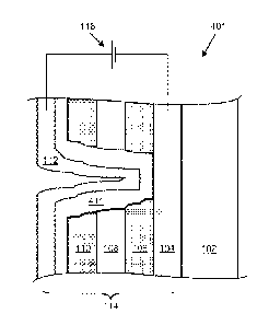
fabrication will be presented. Figures lA and 1B are schematic cross-sections
of an
electrochromic device, 100, showing a common structural motif for such
devices.
Electrochromic device 100 includes a substrate 102, a conductive layer (CL)
104, an
electrochromic layer (EC) 106, an optional ion conducting (electronically
resistive) layer (IC)
108, a counter electrode layer (CE) 110, and another conductive layer (CL)
112. Elements
104, 106, 108, 110, and 112 are collectively referred to as an electrochromic
stack, 114. A
voltage source, 116, operable to apply an electric potential across
electrochromic stack 112
effects the transition of the electrochromic device from, e.g., a bleached
state (refer to Figure
1A) to a colored state (refer to Figure 1B).
The order of layers may be reversed with respect to the substrate. That is,
the layers
may be in the following order: substrate, conductive layer, counter electrode
layer, ion
conducting layer, electrochromic material layer, and conductive layer. The
counter electrode
layer may include a material that is electrochromic or not. If both the
electrochromic layer
and the counter electrode layer employ electrochromic materials, one of them
should be a
cathodically coloring material and the other should be an anodically coloring
material. For
example, the electrochromic layer may employ a cathodically coloring material
and the
counter electrode layer may employ an anodically coloring material. This is
the case when
the electrochromic layer is a tungsten oxide and the counter electrode layer
is a nickel
tungsten oxide.
12
Date Recue/Date Received 2020-12-23
The conductive layers commonly comprise transparent conductive materials, such
as
metal oxides, alloy oxides, and doped versions thereof, and are commonly
referred to as
"TCO" layers because they are made from transparent conducting oxides. In
general,
however, the transparent layers can be made of any transparent, electronically
conductive
material that is compatible with the device stack. Some glass substrates are
provided with a
thin transparent conductive oxide layer such as fluorinated tin oxide,
sometimes referred to as
"TEC."
Device 100 is meant for illustrative purposes, in order to understand the
context of
embodiments described herein. Methods and apparatus described herein are used
to identify
and reduce defects in electrochromic devices, regardless of the structural
arrangement of the
electrochromic device.
During normal operation, an electrochromic device such as device 100
reversibly
cycles between a bleached state and a colored state. As depicted in Figure 1A,
in the
bleached state, a potential is applied across the electrodes (transparent
conductor layers 104
and 112) of electrochromic stack 114 to cause available ions (e.g. lithium
ions) in the stack to
reside primarily in the counter electrode 110. If electrochromic layer 106
contains a
cathodically coloring material, the device is in a bleached state. In certain
electrochromic
devices, when loaded with the available ions, counter electrode layer 110 can
be thought of as
an ion storage layer.
Referring to Figure 1B, when the potential on the electrochromic stack is
reversed, the
ions are transported across ion conducting layer 108 to electrochromic layer
106 and cause
the material to enter the colored state. Again, this assumes that the
optically reversible
material in the electrochromic device is a cathodically coloring
elcctrochromic material. In
certain embodiments, the depletion of ions from the counter electrode material
causes it to
color also as depicted. In other words, the counter electrode material is
anodically coloring
electrochromic material. Thus, layers 106 and 110 combine to synergistically
reduce the
amount of light transmitted through the stack. When a reverse voltage is
applied to device
100, ions travel from electrochromic layer 106, through the ion conducting
layer 108, and
back into counter electrode layer 110. As a result, the device bleaches.
Some pertinent examples of electrochromic devices are presented in the
following US
patent applications: US Patent Application No. 12/645,111, filed December 22,
2009;
US Patent Application No. 12/772,055, filed April 30, 2010; US Patent
Application
No. 12/645,159, filed December 22, 2009; US Patent
13
Date Recue/Date Received 2020-12-23
WO 2014/124303 PCT/US2014/015374
Application No. 12/814,279, filed June 11,2010; and US Patent Application No.
13/462,725,
filed May 2, 2012.
Electrochromic devices such as those described in relation to Figures lA and
1B are
used in, for example, electrochromic windows. For example, substrate 102 may
be
architectural glass upon which electrochromic devices are fabricated.
Architectural glass is
glass that is used as a building material. Architectural glass is typically
used in commercial
buildings, but may also be used in residential buildings, and typically,
though not necessarily,
separates an indoor environment from an outdoor environment. In certain
embodiments,
architectural glass is at least 20 inches by 20 inches, and can be much
larger, e.g., as large as
about 72 inches by 120 inches.
As larger and larger substrates are used for electrochromic windows it is
desirable to
minimize defects in the electrochromic device, because otherwise the
performance and visual
quality of the electrochromic windows will suffer. The embodiments described
herein may
mitigate defeetivity in electrochromic windows.
In some embodiments, electrochromic glass is integrated into an insulating
glass unit
(IGU). An insulating glass unit includes multiple glass panes assembled into a
unit, generally
with the intention of maximizing the thermal insulating properties of a gas
contained in the
space formed by the unit while at the same time providing clear vision through
the unit.
Insulating glass units incorporating electrochromic glass are similar to
insulating glass units
currently known in the art, except for electrical terminals for connecting the
electrochromic
glass to voltage source.
DEFECTIVITY IN ELECTROCHROMIC DEVICES
As used herein, the term "defect" refers to a defective point or region of an
electrochromic device. Typically, defects are electrical shorts or pinholes.
Further, defects
may be characterized as visible or non-visible. In general, a defect in an
electrochromic
device, and sometimes an area around the defect, does not change optical state
(e.g., color) in
response to an applied potential that is sufficient to cause non-defective
regions of the
electrochromic device to color or otherwise change optical state. Often a
defect will be
manifest as visually discernible anomalies in the electrochromic window or
other device.
Such defects are referred to herein as "visible" defects. Other defects are so
small that they
are not visually noticeable to the observer in normal use (e.g., such defects
do not produce a
noticeable light point or "pinhole" when the device is in the colored state
during daytime).
14
Date Recue/Date Received 2020-12-23
WO 2014/124303 PCT/US2014/015374
A short is a localized electronically conductive pathway spanning the ion
conducting
layer (e.g., an electronically conductive pathway between the two transparent
conducting
layers). Typically, a defect causing a visible short will have a physical
dimension on the
order of tens micrometers, sometimes less, which is a relatively small defect
from a visual
perspective. However, these relatively small defects result in a visual
anomaly, the "halo", in
the colored electrochromic window that are, for example, about 1 centimeter in
diameter,
sometimes larger. Halos can be reduced significantly by isolating the defect,
for example by
circumscribing the defect via a laser scribe or by ablating the material
directly without
circumscribing it. For example, a circular, oval, triangular, rectangular, or
other shaped
perimeter is ablated around the shorting defect thus electrically isolating it
from the rest of
the functioning device. The circumscription may be only tens, a hundred, or up
to a few
hundred micrometers in diameter. By circumscribing, and thus electrically
isolating the
defect, the visible short will resemble only a small point of light to the
naked eye when the
window is colored and there is sufficient light on the other side of the
window. When ablated
directly, without circumscription, there remains no EC device material in the
area where the
electrical short defect once resided. Rather, there is a hole through the
device and at the base
of the hole is, for example, the float glass or the diffusion barrier or the
lower transparent
electrode material, or a mixture thereof. Since these materials are all
transparent, light may
pass through the base of the hole in the device. Depending on the diameter of
a
circumscribed defect, and the width of the laser beam, circumscribed pinholes
may also have
little or no electrochromic material remaining within the circumscription (as
the
circumscription is typically, though not necessarily, made as small as
possible). Such
mitigated short defects manifest as pin points of light against the colored
device, thus these
points of light are commonly referred to as "pinholes." Isolation of an
electrical short by
circumscribing or direct ablation would be an example of an intentionally-made
pinhole
formed to convert a halo into a much smaller visual defect. Pinholes may also
arise as a
natural result of defects in the optical device. In either case, they are to
be avoided if possible.
A pinhole is a region where one or more layers of the electrochromic device
are
missing or damaged so that electrochromism is not exhibited. Pinholes are not
electrical
shorts, and, as described above, they may be the result of mitigating an
electrical short in the
device. In certain embodiments, a pinhole has a defect dimension of between
about 25
micrometers and about 300 micrometers, typically between about 50 micrometers
and about
150 micrometers, thus it is much harder to discern visually than a halo.
Typically, in order to
Date Recue/Date Received 2020-12-23
WO 2014/124303 PCT/US2014/015374
reduce the visible perception of pinholes resulting from mitigation of halos,
one will limit the
size of a purposely-created pinhole to about 100 micrometers or less.
In some cases, an electrical short is created by a conductive particle lodging
in and/or
across the ion conducting layer, thereby causing an electronic path between
the counter
electrode layer and the electrochromic layer or the transparent conducting
layer associated
with either one of them. A defect may also be caused by a particle on the
substrate on which
the electrochromic stack is fabricated. When such a particle causes layer
delamination due to
stresses imparted by the particle, this is sometimes called "pop-off. " In
other instances, the
layers do not adhere to the substrate properly and delaminate, interrupting
the flow of ions
and/or electrical current within the device. These types of defects are
described in more
detail below in relation to Figures 2 and 3A ¨ 3D. A delamination or pop-off
defect can lead
to a short if it occurs before a transparent conducting layer or associated EC
or CE layer is
deposited. In such cases, the subsequently deposited transparent conducting
layer or EC/CE
layer will directly contact an underlying transparent conducting layer or
CE/EC layer
providing direct electronic conductive pathway. A few examples of defect
sources are
presented in the table below. The table below is intended to provide examples
of mechanisms
that lead to the different types of visible and non-visible defects. It is not
exhaustive.
Additional factors exist which may influence how the EC window responds to a
defect within
the stack.
Particle
Location Worst Case Failure Effect
on substrate pops off leaving pinhole pinhole
on first
Transparent pops off allowing TCL- visible short
conductive TCL short voltage drop
layer
Pops off allowing TCL- visible short
on EC layer
EC-TCL short voltage drop
on IC layer pops off leaving pinhole pinhole
on CE layer pops off leaving pinhole pinhole
It is believed that problematic shorts are frequently those in which a
particle contacts
the partially fabricated device before, during, or immediately after a first
electrochromic layer
is deposited on a substrate, and then remains in place until immediately
before, during or
16
Date Recue/Date Received 2020-12-23
WO 2014/124303 PCT/US2014/015374
after deposition of the second transparent conductive layer. As explained more
fully below,
such shorts may be the result of particles attached to the substrate upon
entry into the
electrochromic deposition chamber, or particles that become attached during
deposition of a
cathodic electrochromic layer such as a layer of tungsten oxide or become
attached
immediately after deposition of the first electrochromic layer but before any
substantial
amount of the next electrochromic layer is deposited. As explained, the
substrate may or may
not have a transparent conductive layer provided thereon when the substrate
enters the
deposition apparatus. Problematic shorts may also be introduced by particles
that contact the
partially fabricated device during lithiation, such as lithiation performed
after or during
deposition of the second electrochromic layer.
As noted above, in the case of a visible short the defect will appear as a
light central
region (when the device is in the colored state) with a diffuse boundary such
that the device
gradually darkens with distance from the center of the short. If there are a
significant number
of electrical shorts (visible or non-visible) concentrated in an area of an
electrochromic
device, they may collectively impact a broad region of the device whereby the
device cannot
switch in such region. This is because the potential difference between the EC
and CE layers
in such regions cannot attain a threshold level required to drive ions across
the ion conductive
layer. It should be understood that leakage current may result from sources
other than short-
type defects. Such other sources include broad-based leakage across the ion
conducting layer
and edge defects such as roll off defects and scribe line defects. The
emphasis here is on
leakage caused only by points of electrical shorting across the ion conducting
layer in the
interior regions of the electrochromic device. These shorts cause visible
defects that should
be minimized for the electrochromic pane to be acceptable for use in an
electrochromic
window. Conventionally, the visual defects are identified and mitigated prior
to assembly of
the pane into an 1GU or mitigated in an IGU prior to assembly of the IGU in an
architectural
facade. However, these are expensive and time consuming procedures.
Figure 2 is a schematic cross-section of an electrochromic device, 200, with a
particle,
205, in the ion conducting layer causing a localized defect in the device. In
this example,
electrochromic device 200 includes the same layers as described in relation to
Figures 1A and
1B. Voltage source 116 is configured to apply a potential to electrochromic
stack 114 as
described above, through suitable connections (e.g., bus bars) to conductive
layers 104 and
112.
In this example, ion conducting layer 108 includes a conductive particle, 205,
or other
artifact causing a defect. Conductive particle 205 results in a short between
electrochromic
17
Date Recue/Date Received 2020-12-23
WO 2014/124303 PCT/US2014/015374
layer 106 and counter electrode layer 110. In this example, particle 205 spans
the thickness
of the IC layer 108. Particle 205 physically impedes the flow of ions between
electrochromic
layer 106 and counter electrode layer 110, and also, due to its electrical
conductivity, allows
electrons to pass locally between the layers, resulting in a transparent
region 210 in
electrochromic layer 106 and a transparent region 220 in counter electrode
layer 110.
Transparent region 210 exists when the remainder of layers 110 and 106 are in
the colored
state. That is, if electrochromic device 200 is in the colored state,
conductive particle 205
renders regions 210 and 220 of the electrochromic device unable to enter into
the colored
state. Sometimes such visible defect regions arc referred to as
"constellations" or "halos"
because they appear as a series of bright spots (or stars) against a dark
background (the
remainder of the device being in the colored state). Humans will naturally
direct their
attention to the halos and often find them distracting or unattractive.
Embodiments described
herein reduce such visible defects. Pinhole defects may or may not be deemed
worthy of
repair, as they can be nearly indiscernible to the naked eye by most
observers.
As mentioned above, visible short defects can also be caused by particles
popping off,
e.g. during or after fabrication of the electrochromic device, thereby
creating damaged areas
in the electrochromic stack, through one or more layers of the stack. Pop-off
defects are
described in more detail below.
Figure 3A is a schematic cross-section of an electrochromic device, 300, with
a
particle 305 or other debris on conductive layer 104 prior to depositing the
remainder of the
electrochromic stack. Electrochromic device 300 includes the same components
as
electrochromic device 100. Particle 305 causes the layers in the
electrochromic stack 114 to
bulge in the region of particle 305, due to conformal layers 106-110 being
deposited
sequentially over particle 305 as depicted (in this example, conductive layer
112 has not yet
been deposited). While not wishing to be bound by a particular theory, it is
believed that
layering over such particles, given the relatively thin nature of the layers,
can cause stress in
the area where the bulges are formed. More particularly, in each layer, around
the perimeter
of the bulged region, there can be defects in the layer, e.g. in the lattice
arrangement or on a
more macroscopic level, cracks or voids. One consequence of these defects may
be, for
example, an electrical short between electrochromic layer 106 and counter
electrode layer
110 and/or loss of ion conductivity in layer 108. Roll off under the particle
is another
potential source of shorting. These defects are not depicted in Figure 3A,
however.
Referring to Figure 3B, another consequence of defects caused by particle 305
is
called a "pop-off." In this example, prior to deposition of conductive layer
112, a portion
18
Date Recue/Date Received 2020-12-23
WO 2014/124303 PCT/US2014/015374
above the conductive layer 104 in the region of particle 305 breaks loose,
carrying with it
portions of electrochromic layer 106, ion conducting layer 108, and counter
electrode layer
110. The "pop-off' is piece 310, which includes particle 305, a portion of
electrochromic
layer 106, as well as ion conducting layer 108 and counter electrode layer
110. The result is
an exposed area of conductive layer 104 at the bottom of the trench left when
piece 310
popped out of the layered stack of materials. It is believed that certain
process operations
tend to promote pop-offs. One such operation is lithium deposition. Figure 3C
depicts a
"large- format particle 320 formed in stack 300. Such particle spans the
thickness of multiple
layers (in this example electrochromic layer 106, ion conducting layer 108,
and counter
electrode layer 110). While portions of layers 106, 108, and 110 form on top
of particle 320,
they effectively form part of the particle itself, which protrudes above the
top of layer 110. In
some cases, particle 320 naturally pops off without the application of a
particle ejection
promoting step such as lithiation. In other cases, particle 320 is removed by
use of a particle
removal step purposely applied to remove particles. Examples of such steps are
described
below and include contact adhesion techniques, electrostatic approaches, and
thermal or
pressure treatments, as well as lithiation, which serve two purposes.
In some cases, a short type defect is produced underneath an overhanging area
of
particle 320. Such defect may result from roll-off of the subsequently
deposited layers, one
after the other. For example, the first electrochromic layer 106 may extend
only a limited
distance under the particle overhang, while ion conducting layer 108 extends a
little further
under the overhang, counter electrode 110 extends still a little further, and
finally, the second
transparent conductive layer extends ever further, such that its edge contacts
the underlying
first transparent conductive layer. This conductive layer to conductive layer
contact produces
a short-type defect. The short exists regardless of whether particle 320 ever
pops off or is
otherwise dislodged. Such shorts are typically mitigated via circumscription
with a laser to
isolate the defect and create a small, and more acceptable, pinhole.
Referring to Figure 3D, and referring back to Figure 3B, after pop-off and
once
conductive layer 112 is deposited, an electrical short is formed where
conductive layer 112
comes in contact with conductive layer 104. This electrical short would leave
a transparent
region in electrochromic device 300 when it is in the colored state, similar
in appearance to
the visual defect created by the short described above in relation to Figure
2.
Pop-off defects due to particles or debris on the substrate, ion conducting
layer, and
on the counter electrode layer may also cause pinhole defects. Also, if a
contaminate particle
19
Date Recue/Date Received 2020-12-23
is large enough and does not cause a pop-off, it might be visible when the
electrochromic
device is in the bleached state.
The description above, as described in relation to Figures 1A, 1B, 2, and 3A-
D,
presumes that there is a distinct ion conducting (electronically resistive)
layer sandwiched
between an electrochromic layer and a counter electrode layer in
electrochromic devices.
The description is only meant to be illustrative of how a particle can create
a short related
defect. That is, there are electrochromic devices where a distinct
electronically resistive and
ion conducting layer does not exist, but rather an interfacial region that
serves as an ion
conductive layer exists at the interface of the electrochromic and counter
electrode layers.
Electrochromic devices having this architecture are described in U.S. Patent
applications,
serial numbers 12/772,055 filed 4/30/2010, 12/772,075 filed 4/30/2010,
12/814,277 filed
6/11/2010, 12/814,279 filed 6/11/2010 and 13/166,537 filed 6/22/2011, each
entitled,
"Electrochromic Devices," each having inventors Wang et al. Thus particles can
cause shorting
defects in these devices as well, e.g., where the particle exists at and/or
crosses the interface
between the electrochromic and counter electrode layers and/or creates pop-off
type defects as
described. Such devices are also susceptible to other defect types described
herein, despite not
having a distinct IC layer as in conventional devices.
Thus, three types of defects are of primary concern with regard to
electrochromic
windows: (1) visible pinholes, (2) visible shorts, and (3) non-visible shorts.
A visible pinhole
will have a defect dimension of at least about 100 um, and manifest as a very
small point of
Eight when the window is colored, sometimes barely discernible to the naked
eye, but visible
upon close scrutiny. Typically, though not necessarily, a visible short will
have defect
dimension of at least about 3 micrometers resulting in a region, e.g of about
1 cm in
diameter, which as mentioned is sometimes referred to as a "halo," where the
electrochromic
effect is perceptibly diminished. These halo regions can be reduced
significantly by isolating
the defect causing the visible short so that to the naked eye the visible
short will resemble
only a visible pinhole. Non-visible shorts can affect switching performance of
the
electrochromic device, by contributing to the overall leakage current of the
device, but do not
create discernible points of light or halos when the window is in a colored
state.
Visible shorts produce a halo when the device is darkened. A halo is a region
in the
device where an electrical short across the electrochromic stack causes an
area around the
short to drain current into the short and therefore the area surrounding the
short is not
Date Recue/Date Received 2020-12-23
WO 2014/124303 PCT/US2014/015374
darkened. As mentioned, these regions can be up to about 1 cm in diameter, and
thus present
a problem by making the electrochromic window, when colored, unattractive to
the observer.
This frustrates the purpose of having windows that can operate in a colored
mode.
Conventionally visible short defects are mitigated after fabrication of the
electrochromic device, but while still in the production facility, for
example, prior to
installation in an insulated glass unit. For example, individual
electrochromic panes are
characterized by first applying temporary bus bars and then coloring the
electrochromic
device. Visual defects such as halos are identified and then mitigated, for
example, laser
circumscribed to isolate them and remove the halo effect, which leaves
smaller, less
discernible, pinhole defects. As described above, conventionally, at least
two, large,
dedicated apparatus, are used to carry out identification and mitigation of
visual defects.
However, defects can form in the electrochromic devices after the devices
leave the
production facility due to, for example, the inherent stresses in
electrochromic devices (e.g.
see above) and/or stresses applied to the windows during normal use such as
installation,
pressure differential between interior and exterior space, impacts that do not
break the
window pane and the like. Conventionally, for electrochromic windows already
installed in a
vehicle or building, mitigating such defects would not be done, rather the
unit would be
replaced in the field. This can be very expensive.
As mentioned, the methods and devices herein mitigate the effects of defects.
In one
embodiment, the number of visible pinhole defects is no greater than about
0.04 per square
centimeter. In another embodiment, the number of visible pinhole defects is no
greater than
about 0.02 per square centimeter, and in more specific embodiments, the number
of such
defects is no greater than about 0.01 per square centimeter. In one
embodiment, the number
of short-related defects visible when the device is colored is no greater than
about 0.005 per
square centimeter. In another embodiment, the number of short-related defects
visible when
the device is colored is no greater than about 0.003 per square centimeter,
and in more
specific embodiments, the number of such defects is no greater than about
0.001 per square
centimeter. In a further embodiment, the number of short-related defects
visible when the
device is colored is no greater than about 0.0005 per square centimeter. In
one embodiment,
the total number of visible defects, pinholes and short-related pinholes
created from isolating
visible short-related defects, is less than about 0.1 defects per square
centimeter, in another
embodiment less than about 0.08 defects per square centimeter, in another
embodiment less
than about 0.05 defects per square centimeter, in another embodiment less than
about 0.01
defects per square centimeter, and in another embodiment less than about 0.045
defects per
21
Date Recue/Date Received 2020-12-23
WO 2014/124303 PCT/US2014/015374
square centimeter (less than about 450 defects per square meter of window). In
some cases,
the total number of visible defects, pinholes and short-related pinholes
created from isolating
visible short-related defects, is less than about 0.005 defects per square
centimeter.
In some embodiments, the number of non-visible electrical short defects
results in
leakage currents of less than about 20 ittA/cm2 at 2V bias. These values
apply across the
entire face of the electrochromic device (i.e., there is no region of the
device (anywhere on
the device) having a defect density greater than the recited value).
In some embodiments, the electrochromic device has no visible defects greater
than
about 1.6 mm in diameter (the largest transverse dimension of the defect). In
another
embodiment, the device has no visible defects greater than about 0.5 mm in
diameter, in
another embodiment the device has no visible defects greater than about 100
!Am in diameter.
STRUCTURES WITH DEFECT-MITIGATING INSULATING LAYERS
Various disclosed embodiments concern the insertion of an additional layer in
the
electrochromic device stack. This additional layer serves the primary role of
providing an
insulating layer between two conductive layers that might otherwise short
circuit if a particle
is ejected from the device stack during fabrication or remains on the surface
all the way
through the fabrication process, leading to roll off shorting. For example, if
a particle is
introduced during fabrication of the first transparent conductive layer or the
first of the
electrochromic and counter electrode layers, the particle may be ejected prior
to deposition of
the second transparent conductive layer, which will produce a short circuit.
See rows 2 and 3
of the above table.
In one implementation, a resistive layer, sometimes referred to as a defect-
mitigating
insulating layer, is deposited at a point in the device fabrication process
that is after formation
of the first transparent conductive layer and before formation of the second
transparent
conductive layer. As should be apparent from the above discussion, direct
contact between
two transparent conductive layers of opposite polarity creates a short
circuit. Similarly, direct
contact between one of the transparent conductive layers and the
electrochromic or counter
electrode layer having a polarity opposite that of the conductive layer it
contacts produces a
short circuit. To avoid any of these types of short circuit, the defect-
mitigating insulating
layer is formed after particle ejection that exposes the lower transparent
conductive layer or
the electrochromic or counter electrode layer of polarity opposite that of the
upper transparent
conductive layer. The insulating layer is typically formed prior to formation
of the second
22
Date Recue/Date Received 2020-12-23
transparent conductive layer. In certain embodiments, the insulating layer is
deposited in a
process operation that is the next operation after the execution of an
operation that has a
propensity to cause particle ejections. In one example, the insulating layer
is deposited
immediately after deposition of the first deposited layer of the
electrochromic and counter
electrode layers. For example, if the electrochromic layer is deposited prior
to the counter
electrode layer, the insulating layer is deposited immediately after the
electrochromic layer is
deposited. In such cases, the insulating layer is made from a material that is
not a
conventional ion conducting layer. In another example, the insulating layer is
deposited
immediately after tithiation of the first deposited layer of the
electrochromic and counter
electrode layers. In another example, the insulating layer is deposited
immediately after an
ion conducting layer is deposited. In another example, the insulating layer is
deposited
immediately after the second deposited layer of the electrochromic and counter
electrode
layers. In another example, the insulating layer is deposited immediately
after lithiation of
the second deposited layer of the electrochromic and counter electrode layers.
Figure 4A illustrates one example of an electrochromic device 401 having a
defect-
mitigating insulating layer 411 disposed in contact with the second
transparent conductive
layer 112 and between conductive layer 112 and counter electrode layer 110, IC
layer 108,
electrochromic layer 106 as well as first transparent conductive layer 104
Insulating layer 411
thus prevents the second transparent conductive layer from shorting to the
first transparent
conductive layer as well as shorting with electrochromic layer 106. As shown
in Figure 4A, a
stack of layers is formed on a substrate 102. The device has first and second
transparent
conductive layers 104 and 112 that would short as in the example of Figure 3C
except that a
defect-mitigating insulating layer 411 is provided between them. The
composition and other
features of layer 411 are described below.
It should be noted that various features of device 401 are effectively
identical to those
of device 300 in Figure 3D. Elements of Figures 4A, B. and/or C having the
same reference
numerals as elements of Figure 3D may be considered to be essentially the same
elements as
their counterparts in Figure 3D. It should be understood that implementations
including an
insulating layer such as 411 need not employ the stack construction depicted
in Figure 4A.
For example, various implementations do not include a distinct ion conducting
layer 108 as
shown. Alternatives to use of a distinct ion conducting layer are described in
US Patent
Applications 12/772,055, 12/814,279, and 13/462,725.
23
Date Recue/Date Received 2020-12-23
WO 2014/124303 PCT/US2014/015374
In some implementations, the counter electrode layer 110 is lithiated
immediately
before the insulating layer 411 is formed. One example of a fabrication
procedure for
forming the structure of Figure 4A is presented in Figure 5B.
Electrochromic layer 106 may contain any one or more of a number of different
electrochromic materials, including metal oxides. Examples of such metal
oxides include
tungsten oxide (W03), molybdenum oxide (Mo03), niobium oxide (Nb2O5), titanium
oxide
(TiO2), copper oxide (Cu0), iridium oxide (Ir203), chromium oxide (Cr203),
manganese
oxide (Mn203), vanadium oxide (V205), nickel oxide (Ni203), cobalt oxide
(Co203) and the
like. In some embodiments, the metal oxide is doped with one or more dopants
such as
lithium, sodium, potassium, molybdenum, vanadium, titanium, and/or other
suitable metals or
compounds containing metals. Mixed oxides (e.g., W-Mo oxide, W-V oxide) are
also used in
certain embodiments.
In some embodiments, tungsten oxide or doped tungsten oxide is used for
electrochromic layer 106. In one embodiment of the invention, the
electrochromic layer is
made substantially of WOõ, where "x" refers to an atomic ratio of oxygen to
tungsten in the
electrochromic layer, and xis between about 2.7 and 3.5. It has been suggested
that only sub-
stoichiometric tungsten oxide exhibits electrochromism; i.e., stoichiometric
tungsten oxide,
W03, does not exhibit electrochromism. In a more specific embodiment, WO,,
where x is
less than 3.0 and at least about 2.7 is used for the electrochromic layer. In
another
embodiment, the electrochromic layer is W0x, where x is between about 2.7 and
about 2.9.
In certain embodiments, the tungsten oxide is crystalline, nanocrystalline, or
amorphous. In some embodiments, the tungsten oxide is substantially
nanocrystalline, with
grain sizes, on average, from about 5 nm to 50 nm (or from about 5 nm to 20
nm), as
characterized by transmission electron microscopy (TEM).
The thickness of first electrochromic layer 106 depends on the electrochromic
material selected for the electrochromic layer. In some embodiments, the
electrochromic
layer 106 is about 50 nm to 2,000 nm, or about 200 nm to 700 nm. In some
embodiments,
the electrochromic layer is about 300 nm to about 500 nm. The thickness of the
electrochromic layer 106 is also substantially uniform. In one embodiment, a
substantially
uniform electrochromic layer varies only about +10% in each of the
aforementioned
thickness ranges. In another embodiment, a substantially uniform
electrochromic layer varies
only about +5% in each of the aforementioned thickness ranges. In another
embodiment, a
substantially uniform electrochromic layer varies only about +3% in each of
the
aforementioned thickness ranges.
24
Date Recue/Date Received 2020-12-23
While not shown in Figure 4A, the electrochromic and/or counter electrode
layers
may be deposited in two sub-layers. In one embodiment, the electrochromic
layer is divided
into two sub-layers, one having a nominal oxygen concentration and the other
having an
oxygen-rich concentration. For example, the sub-layer closer to transparent
conductive layer
104 contains tungsten oxide having nominal oxygen concentration and the sub-
layer closer to
the counter electrode contains a more oxygen rich form of tungsten oxide. Such
electrochromic layer designs are described in US Patent Application No.
12/814,279.
Referring again to Figure 4A, in electrochromic stack, an ion conducting layer
108
overlays first electrochromic layer 106. On top of ion conducting layer 108 is
counter
electrode layer 110. The counter electrode layer 110 may be implemented as a
second
electrochromic layer. In some embodiments, counter electrode layer 110 is
inorganic and/or
solid. The counter electrode layer may comprise one or more of a number of
different
materials that are capable of serving as reservoirs of ions when the
electrochromic device is
in the bleached state. Thus, the counter electrode layer serves not only as an
ion storage
layer, but also as a complimentary coloring layer.
In some embodiments, suitable materials for the counter electrode
complementary to
W03 include nickel oxide (Ni0), nickel tungsten oxide (NiWO), nickel vanadium
oxide,
nickel chromium oxide, nickel aluminum oxide, nickel manganese oxide, nickel
magnesium
oxide, nickel tantalum oxide, chromium oxide (Cr203), manganese oxide (Mn02),
Prussian
blue. Optically passive counter electrodes comprise cerium titanium oxide
(Ce07-Ti02),
cerium zirconium oxide (Ce02-ZrO2), nickel oxide (NiO), nickel-tungsten oxide
(NiWO),
vanadium oxide (V105), and mixtures of oxides (e.g., a mixture of Ni203and
W03). Doped
formulations of these oxides may also be used, with dopants including, e.g.,
tantalum and
tungsten. Because counter electrode layer 110 contains the ions used to
produce the
electrochromic phenomenon in the electrochromic material when the
electrochromic material
is in the bleached state, the counter electrode preferably has high
transmittance and a neutral
color when it holds significant quantities of these ions.
In some embodiments, nickel-tungsten oxide (NiWO) is used in the counter
electrode
layer (second electrochromic layer). In certain embodiments, the amount of
nickel present in
the nickel-tungsten oxide can be up to about 90% by weight of the nickel-
tungsten oxide. In
a specific embodiment, the mass ratio of nickel to tungsten in the nickel-
tungsten oxide is
between about 4:6 and 6:4 (e.g., about 1:1). In one embodiment, the NiWO is
between about
15% (atomic) Ni and about 60% Ni; between about 10% W and about 40% W; and
between
Date Recue/Date Received 2020-12-23
WO 2014/124303 PCT/US2014/015374
about 30% 0 and about 75% 0. In another embodiment, the NiWO is between about
30%
(atomic) Ni and about 45% Ni; between about 10% W and about 25% W; and between
about
35% 0 and about 50% 0. In one embodiment, the NiWO is about 42% (atomic) Ni,
about
14%W, and about 44% 0.
The counter electrode morphology may be crystalline, nanocrystalline, or
amorphous.
In some embodiments, where the counter electrode layer is nickel-tungsten
oxide, the counter
electrode material is amorphous or substantially amorphous. Substantially
amorphous nickel-
tungsten oxide counter electrodes have been found to perform better, under
some conditions,
in comparison to their crystalline counterparts. The amorphous state of the
nickel-tungsten
oxide may be obtained through the use of certain processing conditions,
described below.
In some embodiments, the thickness of the counter electrode is about 50 nm
about
650 nm. In some embodiments, the thickness of the counter electrode is about
100 nm to
about 400 nm, preferably in the range of about 200 nm to 300 nm. The thickness
of the
counter electrode layer 110 is also substantially uniform. In one embodiment,
a substantially
uniform counter electrode layer varies only about +10% in each of the
aforementioned
thickness ranges. In another embodiment, a substantially uniform counter
electrode layer
varies only about +5% in each of the aforementioned thickness ranges. In
another
embodiment, a substantially uniform counter electrode layer varies only about
+3% in each of
the aforementioned thickness ranges.
In between electrochromic layer 106 and counter electrode layer 110, there is
an ion
conducting layer 108. Ion conducting layer 108 serves as a medium through
which ions are
transported, in the manner of an electrolyte. That is, when the electrochromic
device
transforms between the bleached state and the colored state, ions pass through
the ion
conducting layer. Typically, ion conducting layer 108 is highly conductive to
the relevant
ions for the efectrochromic and the counter electrode layers, but has
sufficiently low electron
conductivity that negligible electron transfer takes place during normal
operation A thin ion
conducting layer with high ionic conductivity permits fast ion conduction and
hence fast
switching for high performance electrochromic devices. In certain embodiments,
the ion
conducting layer 108 is inorganic and/or solid. When fabricated from a
material and in a
.. manner that produces relatively few defects, the ion conductor layer can be
made very thin to
produce a high performance device. In various implementations, the ion
conductor material
has an ionic conductivity of between about 10-6 Siemens/cm or ohm-lcm-1 and
about 10-9
Siemens/cm or ohm-1cm-1 and an electronic resistivity between 5x101 and 1014
ohms-cm.
26
Date Recue/Date Received 2020-12-23
WO 2014/124303 PCT/US2014/015374
Examples of suitable ion conducting layers include silicates, silicon oxides,
tungsten
oxides, tantalum oxides, niobium oxides, and borates. The silicon oxides
include silicon-
aluminum-oxide. The tungsten oxides include tungstates. These materials may be
doped
with different dopants, including lithium. Lithium doped silicon oxides
include lithium
silicon-aluminum-oxide. In some embodiments, the ion conducting layer
comprises a
silicate-based structure. In other embodiments, suitable ion conductors
particularly adapted
for lithium ion transport include, but are not limited to, lithium silicate,
lithium aluminum
silicate, lithium aluminum borate, lithium aluminum fluoride, lithium borate,
lithium nitride,
lithium zirconium silicate, lithium niobate, lithium tungstatc, lithium
borosilicate, lithium
phosphosilicatc, and other such lithium-based ceramic materials, silicas, or
silicon oxides,
including lithium silicon-oxide. Any material, however, may be used for the
ion conducting
layer 108 provided it can be fabricated with low defectivity and it allows for
the passage of
ions between the counter electrode layer 110 to the electrochromic layer 106
while
substantially preventing the passage of electrons.
As mentioned, various embodiments do not include a distinct or deposited ion
conducting layer 108 as shown. In some cases, a transition region or
interfacial region forms
between electrochromic and counter electrode layers deposited in direct
contact with one
another. Such region may be formed in situ ¨ without depositing a separate ion
conducting
material layer ¨ and possess certain characteristics of a conventional ion
conducting layer as
described above.
In certain embodiments, one or both of the conductive layers 104 and 112 is
inorganic
and/or solid. Conductive layers 104 and 112 may be made from a number of
different
materials, including conductive oxides, thin metallic coatings, conductive
metal nitrides, and
composite conductors. Typically, conductive layers 104 and 112 are transparent
at least in
the range of wavelengths where electrochromism is exhibited by the
electrochromic layer.
Transparent conductive oxides include metal oxides and metal oxides doped with
one or
more metals. Examples of such metal oxides and doped metal oxides include
indium oxide,
indium tin oxide, doped indium oxide, tin oxide, doped tin oxide, zinc oxide,
aluminum zinc
oxide, doped zinc oxide, ruthenium oxide, doped ruthenium oxide and the like.
Since oxides
are often used for these layers, they are sometimes referred to as
"transparent conductive
oxide" (TCO) layers. Thin metallic coatings that are substantially transparent
may also be
used. Examples of metals used for such thin metallic coatings include
transition metals
including gold, platinum, silver, aluminum, nickel alloy, and the like. Thin
metallic coatings
based on silver, well known in the glazing industry, are also used. Examples
of nitrides that
27
Date Recue/Date Received 2020-12-23
WO 2014/124303 PCT/US2014/015374
are conductive in some configurations include titanium nitrides, tantalum
nitrides, titanium
oxynitrides, and tantalum oxynitrides. The conductive layers 104 and 112 may
also be
composite conductors. Such composite conductors may be fabricated by placing
highly
conductive ceramic and metal wires or conductive layer patterns on one of the
faces of the
substrate and then over-coating with transparent conductive materials such as
doped tin
oxides or indium tin oxide. Ideally, such wires should be thin enough as to be
invisible to the
naked eye (e.g., about 1001.im or thinner).
The function of the conductive layers is to spread an electric potential
provided by
voltage source 116 over surfaces of the electrochromic stack to interior
regions of the stack,
with very little ohmic potential drop. The electric potential is transferred
to the conductive
layers though electrical connections to the conductive layers. In some
embodiments, bus
bars, one in contact with conductive layer 104 and one in contact with
conductive layer 112,
provide the electric connection between the voltage source 116 and the
conductive layers 104
and 112. The conductive layers 104 and 112 may also be connected to the
voltage source 116
with other conventional means.
In some embodiments, the thickness of conductive layers 104 and 112 is between
about 5 nm and about 10,000 nm. In some embodiments, the thickness of
conductive layers
104 and 112 are between about 10 nm and about 1,000 nm. In other embodiments,
the
thickness of conductive layers 104 and 112 arc between about 10 nm and about
500 nm. In
some embodiments where TEC Glass I'm is used for substrate 102 and conductive
layer 104,
the conductive layer is about 400 nm thick. In some embodiments where indium
tin oxide is
used for conductive layer 11 2, the conductive layer is about 100 nm to 400 nm
thick (280 nm
in one embodiment). More generally, thicker layers of the conductive material
may be
employed so long as they provide the necessary electrical properties (e.g.,
conductivity) and
optical properties (e.g., transmittance). Generally, the conductive layers 104
and 112 are as
thin as possible to increase transparency and to reduce cost. In some
embodiment,
conductive layers are substantially crystalline. In some embodiment,
conductive layers are
crystalline with a high fraction of large equiaxed grains
The thickness of the each conductive layer 104 and 112 is also substantially
uniform.
Smooth layers (i.e., low roughness, Ra) of the conductive layer 104 are
desirable so that other
layers of the electrochromic stack are more compliant. In one embodiment, a
substantially
uniform conductive layer varies by no more than about +10% in each of the
aforementioned
thickness ranges. In another embodiment, a substantially uniform conductive
layer varies by
28
Date Recue/Date Received 2020-12-23
WO 2014/124303 PCT/US2014/015374
no more than about +5% in each of the aforementioned thickness ranges. In
another
embodiment, a substantially uniform conductive layer varies by no more than
about +2% in
each of the aforementioned thickness ranges.
The sheet resistance (Rs) of the conductive layers may also be important
because of
the relatively large area spanned by the layers. In some embodiments, the
sheet resistance of
conductive layers 104 and 112 is about 5 to 30 Ohms per square. In some
embodiments, the
sheet resistance of conductive layers 104 and 112 is about 12 Ohms per square.
In general, it
is desirable that the sheet resistance of each of the two conductive layers be
about the same.
In one embodiment, the two layers each have a sheet resistance of about 10-15
Ohms per
square.
In certain embodiments, the later formed of the counter electrode layer and
the
electrochromic layer is formed in two operations separated by a lithiation
operation. After
the first portion is deposited and then lithiated, the insulating layer 411 is
deposited. Then the
second portion of the counter electrode (or electrochromic layer) is
deposited. Figure 4B
depicts such an embodiment employing an insulating layer to protect against
short circuits
resulting from particle ejections. In this example, an electrochromic device
403 includes a
stack having a first transparent conductive layer 104, an electrochromic layer
106, an optional
ion conducting layer 108, a counter electrode layer 110 and a second
transparent conductive
layer 112, all as described above. Additionally, the device stack includes a
defect-mitigating
insulating layer 411 disposed within the counter electrode layer. As a result,
the counter
electrode layer is divided into an inner portion 110 and an outer portion
110', separated from
one another by layer 411. In an alternate embodiment, the positions of the
electrochromic
layer and the counter electrode layer are reversed, so that the electrochromic
layer is split by
insulating layer 411 and includes an outer portion 106' in contact with the
second conductive
.. layer 112. Typically, though not necessarily, the two portions of the
counter electrode layer
(or counter electrode layer) are compositionally and/or morphologically alike.
Figure 4C illustrates an embodiment in which a portion 413 of the counter
electrode
serves as an insulating layer. Portion 413 is similar in composition to the
main counter
electrode portion 111 but may be more insulating, so much so that is can
prevent a short
between transparent conductive layers 104 and 112 when it is the only layer
between them, as
shown in the Figure 4C. Typically, it is at least as insulating as portion
111. In some
implementations, portion is 413 does not have electrochromic properties, while
portion 111
does.
29
Date Recue/Date Received 2020-12-23
WO 2014/124303
PCT/US2014/015374
As an example, portions 111 and 413 are both nickel tungsten oxide materials,
but
portion 413 has a relatively lower ratio of nickel to tungsten and/or is
deposited under
different conditions. In various embodiments, the main portion 111 of the
counter electrode
layer is deposited and then lithiated. Thereafter, the second portion 413 of
the counter
electrode layer is deposited. In some implementations, first portion 111 has a
thickness of
between about 200 and 500 nm or between 250 and 350 nm (e.g., about 280 nm).
In some
implementations, second portion 413 has a thickness of about 5-30 nm or about
5-20 nm
(e.g., about 10 nm).
There are many possible implementations of a two portion electrochromic layer
in
which one portion serves as a defect-mitigating insulating layer. In many
implementations,
the electrochromic material serving as an insulating layer remains insulating
with charge
insertion (e.g., lithium ion or hydrogen ion insertion). In many embodiments,
the defect
mitigating insulating layer is ionically conductive and accepts and expels
ions as the
electrochromic device cycles between optical states. Tungsten oxide is an
example of an
electrochromic material that becomes ionically conductive in certain states of
charge.
Specifically, tungsten oxide becomes more ionically conductive with increasing
concentrations of lithium ions, increasing in conductivity by orders of
magnitude when
significant concentrations of lithium ions are inserted. For this reason,
tungsten oxide may
not serve as an effective defect-mitigation insulating layer material. By
contrast, nickel
tungsten oxide remains ionically insulating when lithium ions are inserted and
expelled.
Therefore, nickel tungsten oxide can serve as both an electrochromic layer
material and a
defect-mitigating insulating layer as discussed in the context of Figure 4C.
In some implementations, the electrochromic layer and the counter electrode
layer
may be switched in the deposition sequence. In some implementations, for
example, the
counter electrode is deposited first and then the electrochromic layer is
deposited in portions,
with a first portion being more electronically conductive than a second
portion. A lithiation
step may be performed between depositions of the two portions of the
electrochromic layer.
As in the embodiments presented above, the ion conducting layer may be
dispensed with in
some design stacks.
In some implementations, the first electrochromic layer 106 contains tungsten
oxide
in two sub-layers, each substantially composed of WON. The sub-layer
contacting transparent
conducting layer 104 has a value of x that is approximately 2.7-2.8, and the
other sub-layer
has a value of x that is approximately 2.85 to 3.5. The counter electrode
layer 110 contains
electrochromic nickel tungsten oxide having a thickness of about 50 to 300nm.
The
Date Recue/Date Received 2020-12-23
WO 2014/124303 PCT/US2014/015374
insulating layer 413 also contains nickel tungsten oxide but has different
properties as
discussed elsewhere herein. In the implementation described here, it has a
thickness of about
to 100 nm. The second transparent conductive oxide may be indium tin oxide
having a
thickness of about 200 to 450 nm. The device does not have a separately
deposited ion
5 conducting layer between the electrochromic layer 106 and the counter
electrode layer 111.
In some embodiments, two separate defect-mitigating insulating layers are
provided
in the electrochromic device. In one example, both the insulating layers are
disposed
between the transparent conductive layers. See first and second conductive
layers 104 and
112 in Figure 4D. In one embodiment, a first insulating layer is disposed in
contact with first
transparent conductive layer 104. In one embodiment, a second insulating layer
is disposed
in contact with second conductive layer 112. In the embodiment of Figure 4D, a
first
insulating layer 426 is disposed in contact with first transparent conductive
layer 104 and a
second insulating layer 431 is disposed in contact with second transparent
conductive layer
112. In the device of Figure 4D, there is no IC layer (e.g., no IC layer 108)
disposed between
the electrochromic layer (layer 106) and the counter electrode layer (layer
110). In the
depicted embodiment, the stack is fabricated on a substrate 102. It includes
first conductive
layer 104 in direct or indirect contact with substrate 102, first insulating
layer 426 in contact
with layer 104, electrochromic layer 106 in contact with layer 426, counter
electrode layer
110 in contact with layer 106, second insulating layer 431 in contact with
layer 110, and
second transparent conductive layer 112 (e.g., indium tin oxide). In some
embodiments, first
transparent conductive layer 104 is a fluorinated tin oxide layer such at TEC.
In certain embodiments, first insulating layer 426 is or contains tin oxide,
silicon
oxide, nickel tungsten oxide, cerium oxide, aluminum oxide, tantalum oxide,
silicon
aluminum oxide, and/or titanium oxide. In certain embodiments, first
insulating layer 426 is
.. or contains a metal nitride such as titanium nitride, aluminum nitride,
silicon nitride, tantalum
nitride, or tungsten nitride. In some cases, first insulating layer is or
contains titanium
dioxide. Carbide, oxynitride, and oxycarbide analogs may also be used. In
certain
embodiments, first insulating layer 426 is or contains a tin oxide layer or
titanium oxide, an
alumina (aluminum oxide) layer, or layer containing both tin/titanium oxide
and alumina. In
some embodiments, first insulating layer 426 contains a layer of primary
insulating material
with voids or gaps therein. Occupying these voids or gaps is another
insulating material such
a alumina or other material found in a polishing compound. In certain
embodiments, the
second insulating layer 431 has a composition similar to that of counter
electrode layer 110,
but slightly different in order impart greater resistivity.
31
Date Recue/Date Received 2020-12-23
WO 2014/124303 PCT/US2014/015374
In one example, the structure of Figure 4D includes a layer of titanium
dioxide as a
first insulating layer 426 and a layer of non-conductive nickel tungsten oxide
as second
insulating layer 431. Suitable examples of nickel tungsten oxide as a defect
mitigating
insulating layer are described elsewhere herein.
In some cases, glass is provided containing substrate 102, first transparent
conductive
layer 104 and first insulating layer 426. Such products may include TEC
(fluorinated tin
oxide) layer 104 and titanium dioxide or tin oxide as layer 426. Examples of
such products
include Eclipse AdvantageTM products from Pilkington. In some cases, the
thickness of the
defect-mitigating insulating layer is about 10-100 nm thick, or about 15-50nm
thick, or about
20-40nm thick. A product with high quality conductive layers (and optionally a
defect-
insulating layer) such as the TQ product from Pilkington may be used. In this
context, high
quality layers have relative few defects, relatively continuous layers, and/or
relatively low
roughness in comparison to other products. In one implementation, a substrate
containing a
transparent conductive layer and a defect-mitigating insulating layer is
provided as is, without
polishing, prior to depositing layer 106. In other implementations, the
substrate, including
layer 426, is polished prior to fabricating the remainder of the
electrochromic device.
In certain embodiments, the defect-mitigating layer serves to encapsulate and
promote
adhesion of particles that could be ejected as some point. As shown in Figure
4E, for
example, a defect-mitigating layer 461 conformally encapsulates a particle
305. In certain
embodiments, the thickness of the defect-mitigating layer is a substantial
fraction of the size
of the average defect-causing particle. For example, a defect mitigating layer
that serves to
encapsulate particles may be at least about 500 nm thick. In some embodiments,
an
encapsulating layer does not need to be insulating, and it may be preferable
to have it
matched to the properties of the layer it adjoins. Further, if the
encapsulating layer is between
.. or within counter electrode and/or electrochromic layers, then the
encapsulating layer should
permit lithium ion transport and be of a low enough electrical resistance to
not prevent
electrical transport to compensate for lithium transport. In certain
embodiments, the
encapsulating layer is a material identified herein as an electrochromic or
counter electrode
material.
The description of Figures 4A-E pertains to electrochromic devices having at
least
two distinct layers existing in the device stack. In certain embodiments, the
electrochromic
device contains only a single layer of graded composition that serves the
function of an
electrochromic device stack. Figure 4F depicts one such graded element 421
which is part of
an electrochromic device 413. The electrochromic element 421 is a single layer
graded
32
Date Recue/Date Received 2020-12-23
composition, having a cathodically coloring electrochromic region 417, an ion
conducting
region 418, and an anodically coloring counter electrode or second
electrochromic region,
419. The electrochromic element 421 is sandwiched between two transparent
conducting
layers electrodes 104 and 112. Device fabrication in this example may include
depositing
transparent conductive layer 104 on substrate 102, depositing electrochromic
element 421 on
transparent conductive layer 104, followed by depositing transparent
conductive 112 on
electrochromic element 421. Thus, electrochromic device 413 has only three
layers,
electrochromic element 421 sandwiched between transparent conductive layers104
and 112.
The depicted embodiment also includes a defect-mitigating insulating region
451 located in
the second electrochromic region 421. Region 451 serves the same purpose as
the insulating
layers 411 and 413 in Figures 4A-C. Compositionally, region 451 may be similar
to or
identical to layers 411 and /or 413. It may also have a graded composition
similar to that of
other regions of element 421.
A graded electrochromic element may be viewed as a single layer electrochromic
device stack having successive functional regions as opposed to distinct
layers where there is
an abrupt material change between layers and limited material mixing between
successive
layers. Rather, an electrochromic element has successive functional regions
where there is
significant material mixing between each successive functional region. Further
details of a
compositionally graded multi-functional electrochromic element, including
fabrication
details, are presented in US Patent Application No. 13/462,725.
While Figures 4A-E show substrate 102 in direct contact with first transparent
conductive layer 104, this need not be the case. In any of the implementations
described
herein, these layers may be in direct or indirect contact. In some cases,
glass substrates are
provided with coatings or layers interposed between glass substrate 102 and
first conductive
layer 104. Such coatings may be included for purposes of improving thermal
properties,
transmissivity, blocking diffusion, or other optical properties, providing
resistive heating, etc.
In one example, at least two layers are interposed between substrate 102 and
layer 104.
Examples of such materials include silicon oxides and tin oxides. In some
cases, the
substrate includes a tin oxide layer on top of the main glass substrate, a
silicon oxide layer on
top of the tin oxide layer, and a fluorinated tin oxide layer on top of the
silicon oxide layer.
As illustrated in Figures 4A-E, the defect-mitigating layer(s) may be included
in the
electrochromic device stack at various positions. A number of device stack
examples are
presented below. Each is a variation on the following base stack in which the
EC layer is
33
Date Recue/Date Received 2020-12-23
WO 2014/124303 PCT/US2014/015374
optionally tungsten oxide (or a variant thereof) and the CE layer is nickel
tungsten oxide (or a
variant thereof):
Base device stack
First TC layer
Electrochromic layer
Ion conducting layer (optional)
Counter electrode layer
Second TC layer
Stacks in which an ion conducting layer is not present
Option A
First TC layer
Insulating layer
EC layer
CE layer
Second TC layer
Option B
First TC layer
EC layer
Insulating layer
CE layer
Second TC layer
Option C
First TC layer
EC layer
CE layer
Insulating layer
34
Date Recue/Date Received 2020-12-23
WO 2014/124303
PCT/US2014/015374
Second TC layer
Option D
First TC layer
EC layer
Partial CE layer
Insulating layer
Remainder of CE layer
Second TC layer
Option E
First TC layer
EC layer
Partial CE layer (electrochromic)
Remainder of CE layer (non-electrochromic)
Second TC layer
Option F
First TC layer
First insulating layer
EC layer
Second insulating layer
CE layer
Second TC layer
Option G
First TC layer
First insulating layer
EC layer
CE layer
Second insulating layer
Second TC layer
Option H
Date Recue/Date Received 2020-12-23
WO 2014/124303
PCT/US2014/015374
First TC layer
First insulating layer
EC layer
Partial CE layer
Second insulating layer
Remainder of CE layer
Second TC layer
Option I
First TC layer
Insulating Layer
EC layer
Partial CE layer (electrochromic)
Remainder of CE layer (non-electrochromic)
Second TC layer
Stacks in which an ion conducting is present
Option A
First TC layer
Insulating layer
EC layer
IC layer
CE layer
Second TC layer
Option B
First TC layer
EC layer
Insulating layer
IC layer
CE layer
Second TC layer
36
Date Recue/Date Received 2020-12-23
WO 2014/124303
PCT/US2014/015374
Option C
First TC layer
EC layer
IC layer
Insulating layer
CE layer
Second TC layer
Option D
First TC layer
EC layer
Partial IC layer
Insulating layer
Remainder of IC layer
CE layer
Second TC layer
Option E
First TC layer
EC layer
IC layer
Partial CE layer
Insulating layer
Remainder of CE layer
Second TC layer
Option F
First TC layer
EC layer
IC layer
Partial CE layer (electrochromic)
Remainder of CE layer (non-electrochromic)
Second TC layer
37
Date Recue/Date Received 2020-12-23
WO 2014/124303
PCT/US2014/015374
Option G
First TC layer
Insulating layer
EC layer
Insulating layer
IC layer
CE layer
Second TC layer
Option H
First TC layer
Insulating layer
EC layer
IC layer
Insulating layer
CE layer
Second TC layer
Option I
First TC layer
Insulating layer
EC layer
Partial IC layer
Insulating layer
Remainder of IC layer
CE layer
Second TC layer
Option J
First TC layer
Insulating layer
EC layer
IC layer
Partial CE layer
38
Date Recue/Date Received 2020-12-23
WO 2014/124303 PCT/US2014/015374
Insulating layer
Remainder of CE layer
Second TC layer
Option K
First TC layer
Insulating layer
EC layer
IC layer
Partial CE layer (electrochromic)
Remainder of CE layer (non-electrochromic)
Second TC layer
While each of the above options show the electrochromic layer disposed closer
to the
first transparent conductive layer and the counter electrode layer disposed
closer to the
second transparent conductive layer, the order could be reversed in any of the
options.
Figure 4G is a scanning electron micrograph of an electrochromic device having
a
first transparent conductor layer (TCO) 481 disposed on a substrate, an
electrochromic layer
483 disposed on top of TCO 481, an optional ion conductor layer 485 disposed
on the
electrochromic layer, a counter electrode layer 487 disposed on the ion
conductor layer, and a
second transparent conductor layer (TCO) 489. Figure 4G is presented as a
baseline structure
to show various positions of one or more defect-mitigating insulating layers
as illustrated in
Figures 4H-40. Figures 4H through 4K show devices containing only a single
defect-
mitigating insulating layer and Figures 4L through 40 show devices containing
two defect-
mitigating insulating layers.
Figure 4H shows a defect-mitigating insulating layer at a position between the
first
transparent conductive layer 481 and the electrochromic layer 483. Figure 41
shows a defect-
mitigating insulating layer at an intermediate position within electrochromic
layer 483.
Figure 4J shows a defect-mitigating insulating layer at an intermediate
position within
counter electrode layer 487. Figure 4K shows a defect-mitigating insulating
layer at a
position between the second transparent conductive layer 489 and the counter
electrode layer
487.
Figure 4L shows a device with a first defect-mitigating insulating layer at a
position
between the first transparent conductive layer 481 and the electrochromic
layer 483, and a
second defect-mitigating insulating layer at an intermediate position within
counter electrode
39
Date Recue/Date Received 2020-12-23
WO 2014/124303 PCT/US2014/015374
layer 487. Figure 4M shows a device with a first defect-mitigating insulating
layer at a
position between the first transparent conductive layer 481 and the
electrochromic layer 483,
and a second defect-mitigating insulating layer at a position between the
second transparent
conductive layer 489 and the counter electrode layer 487. Figure 4N shows a
device with a
first defect-mitigating insulating layer at an intermediate position within
electrochromic layer
483, and a second defect-mitigating insulating layer at an intermediate
position within
counter electrode layer 487. Figure 40 shows a device with a first defect-
mitigating
insulating layer at an intermediate position within electrochromic layer 483,
and a second
defect-mitigating insulating layer at a position between the second
transparent conductive
layer 489 and the counter electrode layer 487.
PROCESS FLOW EXAMPLES
As explained, an insulating layer is deposited at some point in the device
fabrication
process between formation of the first and second transparent conductive
layers. In certain
embodiments, the insulating layer is deposited as the next layer after the
execution of a
process step that has a significant likelihood of producing a particle
ejection. An example of
a process step that is likely to eject a particle is the introduction of
lithium metal into the
device stack. As discussed below, other process steps can similarly
precipitate ejection.
A device fabrication process 501 is depicted in Figure 5A and represents a
baseline
process that may be modified to include one or more operations of depositing
an insulating
protective layer. Process 501 begins with an operation 503 where a processing
facility or a
pre-processing apparatus receives a substrate. As explained, the substrate may
be a window, a
mirror, or the like. In some implementations, the substrate provided by a
substrate vendor
contains a transparent conductive oxide layer pre-formed. In other
implementations, the
substrate is provided without the transparent conductive oxide layer, in which
case, the
device fabrication process includes a separate operation of forming the
transparent
conductive layer on the substrate.
Continuing with the process flow 501, an operation 505 involves the washing or
otherwise preparing the substrate for device fabrication. This preparation may
include such
operations as cutting the glass to size, grinding the edges or other portions
of the glass,
washing it, tempering it, washing it again, etc. In some implementations, the
preparation
operations include first cutting the glass substrate to size for the final
process, then grinding
the edge of the glass, followed by tempering or other strengthening operation.
In some cases,
the substrate is washed before and/or after tempering. Cutting, grinding and
similar
Date Recue/Date Received 2020-12-23
operations are described in US Patent Application No, 13/456,056, filed April
25, 2012.
Fabrication of the electrochromic device itself begins after the pre-
processing operation 505 is
complete. In certain embodiments, some or all of the device fabrication
operations are
performed under vacuum or other controlled environmental conditions. For
example, an in line
fabrication process may involve passing the substrate through a series of
interconnected
chambers or stations, each associated with a particular process operation and
each integrated
with a vacuum system or other pressure control system. In some embodiments,
the integrated
deposition system includes a substrate holder and transport mechanism operable
to hold the
architectural glass or other substrate in a vertical orientation while in the
plurality of deposition
stations. In some cases, the integrated deposition system includes one or more
load locks for
passing the substrate between an external environment and the integrated
deposition system. In
another embodiment, the plurality of deposition stations include one or more
stations for
depositing any one or more of the electrochromic layer, the ion conducting
layer, the defect-
mitigating insulating layer, and the counter electrode layer. Sputtering or
other physical vapor
deposition systems may be used for depositing any one or more of the
individual layers making
up the electrochromic device. A sputtering system may also be used to deposit
lithium on the
device.
Many types of apparatus may be employed to deposit electrochromic materials
and
electrochromic devices in accordance with the embodiments disclosed herein.
Frequently
one or more controllers are employed in the apparatus to control the
fabrication process.
Those of ordinary skill in the art will appreciate that processes disclosed
herein may employ
various processes involving data stored in or transferred through one or more
computer
systems and/or controllers. Certain embodiments relate to the apparatus,
including associated
computers and microcontrollers, for performing these operations. A control
apparatus may
be specially constructed for the required purposes, or it may be a general-
purpose computer
selectively activated or reconfigured by a computer program and/or data
structure stored in
the computer. The processes presented herein are not inherently related to any
particular
computer or other apparatus. In various embodiments, a controller executes
system control
software including sets of instructions for controlling the timing and
sequence of the
processing steps, processing conditions as described herein, and the like.
In certain embodiments, the controller contains or executes instructions for
directing a
substrate through a series of deposition stations for depositing the layers of
the
electrochromic stack. The controller may specify, inter cilia, the rate and
direction of
41
Date Recue/Date Received 2020-12-23
substrate transfer, the sputter conditions in any station (e.g., pressure,
temperature, sputtering
power, and gas flow rates), and the pre- and post-treatment of a substrate.
The controller may
include specific instructions for polishing and otherwise pretreating the
substrate prior to
deposition. The controller may include specific instructions for substrate
post-treatments
such as thermal or chemical conditioning. Other computer programs, scripts, or
routines
stored on memory devices associated with the controller may be employed in
some
embodiments.
Examples of apparatus for fabricating electrochromic devices are described in
the
following US Patent Applications: 12/645,111, 12/645,159, 13/462,725, and
12/814,279.
If the substrate provided after pre-processing 505 does not include a thin
layer of
transparent conductive material thereon, device fabrication begins by forming
such layer. If
the substrate as provided includes such layer, it may not be necessary to
perform the
operation. Regardless of how the transparent conductive material is formed, a
first
electrochromic layer is deposited on it in an operation 507. In certain
embodiments, the first
electrochromic layer includes a cathodic electrochromic material. In other
embodiments, it
includes an anodic electrochromic material.
In some cases, the substrate is heated prior to deposition of the first
electrochromic
material. The first electrochromic material layer is typically deposited by a
process involving
physical or chemical vapor deposition under vacuum or other controlled
pressure. In a
typical embodiment, the process involves sputtering a target containing
elements contained in
the electrochromic layer. However, in alternative embodiments, the
electrochromic layer is
deposited under ambient pressure such by a solution phase reaction.
In one implementation, the first electrochromic layer contains a cathodically
coloring
electrochromic material deposited in two operations, one providing a sub-layer
of the base
material in a first stoichiometry and the second providing another sub-layer
of the base
material in a second stoichiometry. As an example, the cathodically coloring
electrochromic
material is tungsten oxide, which has a nominal composition of WOõ The first
deposited
sub-layer may have a composition of tungsten oxide in which the value of x is
about 2.7 to
2.8 and the second deposited sub-layer may have a composition of tungsten
oxide in which x
is about 2.85 to 3.5. In one example, the first sub-layer is thicker: for
example, it has a
thickness of about 400 am and the second sub-layer has a thickness of about
100 nm.
After the first electrochromic layer is deposited, the partially fabricated
device is
optionally lithiated as indicated at process block 509. The lithiation
operation involves
42
Date Recue/Date Received 2020-12-23
delivery of lithium metal or lithium ions into the first electrochromic layer.
The lithium may
be provided by sputtering or other suitable process. Certain aspects of
lithium deposition and
the targets used in lithium deposition processes are described in
International Application No.
PCT/US2012/034556, filed April 20, 2012 (designating the US) and in
International
Application No. PCT/US2012/042514, filed June 14, 2012 (designating the US).
The next operation in device fabrication process 501 involves depositing a
second
electrochromic layer (an example of the counter electrode layer generally
described above).
See block 511. As with the deposition of the first electrochromic layer, this
deposition
process may be accomplishing using, e.g., physical or chemical vapor
deposition. If the first
electrochromic layer contains a cathodically coloring electrochromic material,
then the
second electrochromic layer may contain an anodically coloring electrochromic
material. The
opposite is also true. If the first electrochromic layer contains an
anodically coloring
electrochromic material, the second electrochromic layer may contain a
cathodically coloring
electrochromic material. In certain embodiments, the second electrochromic
layer contains
an anodically coloring electrochromic material such as nickel oxide or nickel
doped tungsten
oxide (sometimes referred to as NiW0). In some examples, where nickel tungsten
oxide
serves as the second electrochromic layer, it is formed to a thickness of
between about 200
and 300 rim. In some cases, only one electrochromic layer is used. Ions are
shuttled into and
out of the single electrochromic layer, from and to a non-electrochromic
counterelectrode.
In the example of Figure 5A, no ion conducting layer is separately deposited
between
the first and second electrochromic layer. In alternative embodiments, an ion
conducting
layer is deposited between these layers. Examples of suitable ion conducting
layers include
those presented above in the description of Figure 4A.
After the second electrochromic layer is deposited, the device, which includes
the first
and second electrochromic layers, is lithiated as indicated in operation 513.
The lithiation
may be accomplished as described in the context of operation 509. As
mentioned, lithiation
operations may promote ejection of particles previously embedded in the
partially fabricated
electrochromic device stack. While not depicted in the process flow of Figure
5A, an
insulating protective layer may be deposited after any of the steps that
promote ejection of
particles. Therefore, in certain embodiments, the deposition of the protective
insulating layer
may be performed after lithiation operation 509 or lithiation operation 513.
Returning to the process flow depicted in Figure 5A, after the lithiation of
the device
in 513, the next process operation deposits a second transparent conductive
oxide layer as
43
Date Recue/Date Received 2020-12-23
depicted in an operation 515. At this point, all structures needed for the
basic electrochromic
device have been created. In some embodiments, there is a subsequent post
treatment of the
as deposited device in order to complete the process. See block 517. Examples
of suitable
post-treatment include thermal and/or chemical conditioning operations. Such
operations are
described in US patent number 12/645,111.
Figures 58-5E present variations on the baseline process depicted in Figure
5A. In
each case, the basic process flow from Figure 5A is depicted but with
additional or different
steps for depositing the insulating layer at particular locations in the
process. See e.g.,
operation 521 in Figure 5B and operation 523 in Figure 5C. In Figure 5B, the
insulating
layer is deposited after lithiation operation 513 and before deposition of the
second
transparent conductive layer (operation 515). In Figure 5C, the insulating
layer is deposited
between lithiation operation 509 and deposition of the second electrochromic
layer (operation
511). In various embodiments, the first litiation and the deposition of the
insulating layer are
performed prior to the completion of the first electrochromic layer. Both of
these deposition
operations take place directly after a titillation operation. As explained,
the process is not
limited to this sequence. Other operations that may promote particle ejection
may also
trigger deposition of the insulating layer. Also, the insulating layer may be
deposited
immediately (or soon) after a step that is likely to produce particles or
otherwise have
particles attach to the substrate surface. In such designs, the defect-
mitigating layer may
serve to encapsulate such particles.
In some cases, the insulating layer is deposited intermediate between two
operations
for depositing the second electrochromic layer. The resulting device may have
a structure as
depicted in Figure 4B, for example. In some cases, a lithiation step is
performed after the
first portion of the second electrochromic layer is deposited and before the
insulating layer
and the second portion of the second electrochromic layer are deposited. In
other
embodiments, the first electrochromic layer is divided into two portions, with
the insulating
layer interposed between the two portions.
In other embodiments, the second (or first) electrochromic layer is deposited
in two
portions, with the second portion serving as the defect-mitigating insulating
layer. An
example of a structure resulting from such processes is depicted in Figure 4C
and the
associated description. In some cases, a lithiation operation is performed
after deposition of
the first portion of the electrochromic layer but before deposition of the
second portion of the
layer.
44
Date Recue/Date Received 2020-12-23
WO 2014/124303 PCT/US2014/015374
In some implementations such as those of Figure 4C, the insulating layer
actually
contains a material having a composition that varies only slightly from that
of the material of
the associated electrochromic layer. As an example, the second portion of an
electrochromic
layer contains an insulating material, or at least a material that is at least
as insulating as the
first portion of the electrochromic layer. In some cases, the first portion of
the layer has
electrochromic properties and the second portion of the layer does not have
electrochromic
properties. Such embodiments may have multiple benefits. For example, the
insulating layer
will be quite compatible with the material on which it is deposited. This is
because the
materials are chemically very similar.
In some embodiments, the second electrochromic layer is a nickel tungsten
oxide and
the insulating layer is also a nickel tungsten oxide. However, the main
portion of the second
electrochromic layer and the insulating layer are deposited under different
process conditions.
For example, while both layers may be deposited by a physical vapor deposition
technique
employing sputtering from nickel and tungsten targets, the PVD conditions are
different. In
some cases, the insulating layer is deposited at a lower pressure and/or with
lower oxygen
concentrations than the electrochromic nickel tungsten oxide layer. In some
cases, the
second portion of the insulating layer is deposited at a lower power than the
second
electrochromic layer. Further, the atomic ratio of nickel to tungsten may be
lower in the
insulating layer. In other cases, the atomic ratio of nickel and tungsten is
the same in both
portions of the layer.
In some examples, the ranges of deposition conditions for nickel tungsten
oxide
electrochromic layer (NiW01) and insulating layer (NiW02) are as follows:
NiWO1
1 mTorr < Pressure < 50 mTorr
60% <02% < 100% (volume or molar)
OC < Deposition Temperature <150C
NiWO2
1 mTorr < Pressure < 50 mTorr
40% < 02% < 70%
25C < Deposition Temperature <200C
In other examples, process conditions used to form each of NiWO1 and NiW02 are
as follows:
Date Recue/Date Received 2020-12-23
NiWO1
mTorr < Pressure < 15 mTorr (or 7-12 mTorr)
70% <02% <90% (volume) (or 70-80%)
20C < Deposition Temperature <60C
5
NiWO2
1 mTorr < Pressure < 10 mTorr (or 3-7mTorr)
40% < 02% <60% (or 45-55%)
25C < Deposition Temperature < 60C
Figure 5D presents a flow chart for an embodiment employing deposition of two
separate defect-mitigating insulating layers. The process begins at an
operation 531, where a
substrate is received having a first transparent conducting layer. In certain
embodiments, the
transparent conducting layer is a fluorinated tin oxide layer that is
optionally covered by an
insulating layer of Ti02. Glass substrates having such properties are provided
by Pilkington
of St. Helens, United Kingdom under the brand name Eclipse Advantage"' for
example. The
substrate received in operation 531 may be washed and prepared as described
above. See
operation 533. Next the process involves forming the first insulating layer as
indicated at
operation 535. This layer may be prepared by many different techniques. As
indicated, the
substrate may be provided with both a transparent conductive layer and an
insulating layer
(e.g., fluorinated SnO capped with TiO2). It has been found that in certain
embodiments
electrochromic devices perform better when fabricated on a substrate that has
been polished.
Such polishing may involve, for example, polishing an upper surface of a TiO2
with a
polishing compound containing alumina or other electronically insulating
material. See PCT
Patent Application No. PCT/US2012/057606, titled "OPTICAL DEVICE FABRICATION",
and filed September 27, 2012. While not wishing to be bound by theory, the
alumina or other
insulating material used in polishing may form an insulating layer on the
surface of the first
transparent (conducting?) layer or alumina particles may fill in voids in the
tin oxide or other
insulating material provided with the substrate. In the latter case, the
insulating layer contains
two different materials, one formed on the substrate as received and the other
filling voids in the
first material. In other embodiments, the first insulating layer formed in
operation 535 is
deposited by a conventional deposition process such as physical vapor
deposition or chemical
46
Date Recue/Date Received 2020-12-23
WO 2014/124303 PCT/US2014/015374
vapor deposition. The resulting layer may have the composition of an
insulating layer as
described elsewhere herein.
After the first insulating layer is formed, the process may continue
essentially as
described with reference to Figures 5B and/or 5C. A first electrochromic layer
is deposited in
.. an operation 537, followed by an optional lithiation operation 539.
Thereafter, an ion
conducting layer is optionally deposited or formed in situ, followed by
deposition of a second
electrochromic layer. See operation 541. The device fabricated to this point
is then lithiated
as indicated in operation 543. A second insulating layer is formed in an
operation 545. The
material used to form this second insulating layer may be the same or
different from that used
to form the first insulating layer in operation 535. If the first insulating
layer is provided with
the substrate received by the process or is provided during polishing,
typically the second
insulating layer will have a different composition ¨ or at least a different
morphology ¨ than
the first insulating layer.
After the second insulating layer has been formed, the process deposits a
second
transparent conductive layer. See operation 547. Thereafter an optional post
treatment is
performed as described above. See operation 549.
Figure 5E presents another process of forming a low-defectivity electrochromic
device. The process begins as shown at a block 551 with the receipt of a
substrate having
various layers pre-formed thereon. These layers may include one or more
diffusion barrier
layers such as a tin oxide and a silicon oxide layer, a first transparent
conductive layer such as
a fluorinated tin oxide layer, and a first defect-mitigating insulating layer.
As indicated, the
defect-mitigating insulating layer may include or be titanium oxide, tin
oxide, silicon oxide,
silicon aluminum oxide, tantalum oxide nickel tungsten oxide, various
nitrides, carbides,
oxycarbides, oxynitrides, and variants of any of these, etc.
Upon receiving the substrate, it may be washed and otherwise prepared for
device
fabrication as indicated in block 553. As mentioned above, the preparation may
include
cutting cleaning tempering, etc. Thereafter, as indicated at block 555, the
substrate surface is
optionally polished. Polishing may be performed with, for example, aluminum
oxide, cerium
oxide, or other appropriate polishing material in an appropriate carrier
forming a polishing
slurry or other appropriate polishing formulation. Polishing may serve various
purposes, as
explained above. Included among these purposes are, for example, reducing the
roughness of
the surface and incorporating insulating material into an insulating surface
layer that might
otherwise contain pits, defects, discontinuities, and other sources of
potential electrical shorts.
The polishing material (e.g., alumina or cerium oxide) in the polishing
compound is itself an
47
Date Recue/Date Received 2020-12-23
WO 2014/124303 PCT/US2014/015374
insulating material that fills gaps in an otherwise continuous insulating
layer provided on the
substrate.
After the optional polishing, the first and second electrochromic layers are
deposited
as described above and as indicated in blocks 557 and 561 of Figure 5E.
Thereafter, a particle
removal steps such as lithiation is performed as indicated at block 563. Then,
a second
defect-mitigating insulating layer is formed over the second electrochromic
layer. See block
565. In a particular implementation of the process depicted in Figure 5E, the
second defect-
mitigating insulating layer is a less-electrochromic form of nickel tungsten
oxide. In this
implementation, the second electrochromic layer is an electrochromic form of
nickel tungsten
oxide. The first electrochromic layer may be tungsten oxide deposited in one
or more layers.
As indicated above, in some implementations, a second tungsten oxide layer
formed on top of
a first tungsten oxide layer may have a composition that is super-
stoichiometric in oxygen.
After the second defect-mitigating insulating layer is formed at block 565, a
second
transparent conductive layer is deposited as indicated by block 567.
Thereafter, a post-
treatment such as a thermal conditioning or thermal chemical conditioning is
performed as
described above. See block 569. The process is thus complete for purposes of
this illustration.
The defect mitigating insulating layer may be deposited by a variety of
techniques.
Physical and chemical vapor depositions are typical. In some cases, the
deposition is
conformal; that is, the process deposits an insulating layer that is able to
follow the contours
of the pits and other topology variations created by particle ejections. The
conformality of
the deposition process should allow the layer to follow contours on the order
of micrometers
or nanometers (e.g., tens or hundreds of nanometers). Examples of classes of
deposition
process that permit this are chemical vapor deposition techniques and atomic
layer deposition
(ALD) techniques. Deposition of device layers performed after the insulating
layer is laid
down may likewise be deposited by a particularly conformal process.
While lithiation has been presented in most embodiments as the operation that
promotes particle removal, various other techniques may likewise serve to
promote particle
removal. One of these is "contact cleaning," a process that involves
contacting a layer of a
partially fabricated electrochromic device with a contact roller, strip, or
brush, which sticks to
or attracts particles and then removes them from the device. Typically,
contact cleaning
employs static attraction and/or adhesion to attract remove particles. Some
contact cleaning
products are commercially available, being marketed to the contact sheet
cleaning and web
cleaning industries. In various embodiments, a roller mechanism is used. In
some cases, two
rollers are used: the first one for contacting and removing particles from the
device surface
48
Date Recue/Date Received 2020-12-23
WO 2014/124303 PCT/US2014/015374
and a second roller for contacting the first roller to remove the particles
that were picked up
by the first roller in its most recent rotation. Examples of contact cleaning
products sold for
cleaning bare glass are manufactured by TeknekTm of Renfrewshire, Scotland, UK
and
Technica.
In some implementations, a contact cleaner is integrated with an
electrochromic
device fabrication system. Typically, though not always, the contact cleaner
is deployed
outside the vacuum environment of the system for depositing layers of the
electrochromic
device. In "cut and coat- fabrication process flows, a contact cleaner of a
single size may be
used. In other fabrication flows, contact cleaners of different size are
employed for cleaning
devices fabricated on glass of different sizes.
Another category of particle removal techniques rely on differences in the
thermal
expansion of particles and the substrate layers in which they are embedded.
When the
particle volume expands or contracts relative to the surrounding layers, the
particles may
eject, particularly when the relative volume change is rapid. In some
embodiments, a
mechanism driving the volume change is irradiation of the substrate at
wavelength that is
selectively absorbed by the particles but not the surrounding layer(s), or
vice versa. In some
embodiments, a mechanism driving a relative volume change is a different
coefficient of
thermal expansion of the particles and the surrounding layer(s).
Thermal energy may be delivered in various ways. For example, as mentioned,
the
particles and or the substrate layer(s) may be heated by irradiation. The
irradiation may be
provided at a wavelength or spectrum of wavelengths from the infrared through
ultraviolet
ranges. The irradiation may be provided by one or more lamp, lasers, etc. In
one approach, a
collimated laser beam is passed over a surface of the partially fabricated
electrochromic
device. For example, the beam grazes the surface of the device over the width
of the device.
The beam may propagate in a direction perpendicular or substantially
perpendicular to the
direction of travel of the substrate carrying the electrochromic device. In
another approach, a
laser beam is focused on the device and moved in a raster scan over the
surface.
In some embodiments, thelmal energy is provided by heating the substrate by a
non-
radiative mechanism such as passing heated gas over the surface of the
substrate/device
and/or passing the substrate/device over a heated element such as a roller. In
one
implementation, the heated element is heated by resistive heating.
In another approach to particle removal, electrostatic force is applied to the
partially
fabricated electrochromic device. This may be accomplished by, e.g.,
contacting the device
with a plasma or applying a charge to the substrate containing the device. In
one
49
Date Recue/Date Received 2020-12-23
WO 2014/124303 PCT/US2014/015374
embodiment, a two stage process is employed. In the first stage, the particles
are charged by
exposure to a plasma. Then, in the second stage, the substrate with charged
particles receives
an electrical charge, which causes the charged particles to eject. For
example, an electrical
contact is made to a conductive or partially conductive layer of the substrate
and charge is
applied to the device through the contact. In some implementations, the
substrate is
contacted with a charge of the same sign as the charge applied to the
particles by contact with
the plasma.
In a further approach, the partially fabricated electrochromic device is
exposed to a
supercritical fluid such as supercritical carbon dioxide. Supercritical fluids
are quite effective
at dislodging and removing particles. The fluid may include a supercritical
solvent such as
supercritical carbon dioxide with one or more additives contained therein to
improve the
cleaning power or other property of the fluid. The supercritical fluid may be
brought into
contact with the partially fabricated electrochromic device using any of a
number of
processes. For example, the device may be immersed or passed through the
supercritical
fluid. The fluid itself may be provided in a quiescent or flowing state. In
various
embodiments, some convection will be employed. For example, the supercritical
fluid may
flow through a substrate contact chamber driven by a pump in a recirculation
loop. In certain
embodiments, the supercritical fluid is provided as a cryogenic aerosol. The
fluid may be
sprayed on the device as the device or a spray nozzle (or spray gun) moves
with respect to the
other.
In still another approach, particles are dislodged and/or removed by applying
acoustic
energy to the partially fabricated electrochromic device. The acoustic energy
may be
provided at any of a number of frequencies, including megasonic, supersonic,
ultrasonic, etc.
In certain embodiments, a vibration source is directly coupled to the
substrate. In certain
embodiments, a vibration source is directly coupled to a fluid in contact with
the
substrate/device.
Another removal technique involves ionized air blow off, optionally with an
air knife.
Yet another technique involves etch-back of a layer of the device containing
particles. The
etch-back may be accomplished with a plasma (e.g., a fluorine or oxygen
containing plasma),
by using ion milling, etc. The particles may be removed by the etch-back
process or merely
dislodged. In the latter case, a separate particle removal operation may be
applied after etch-
back. Such process may include one or more other process described above such
as applying
a charge to the substrate, contacting the substrate with a supercritical
fluid, or selectively
heating the particles.
Date Recue/Date Received 2020-12-23
WO 2014/124303 PCT/US2014/015374
When lithiation is employed as a particle removal technique, it may be
implemented
in various formats. For example, the lithium may be delivered in a single dose
or in multiple
doses, sometimes to different layers of the device, such as to the
electrochromic and counter
electrode layers. In some embodiments, all the lithium needed for the device
is delivered in a
single operation. For example, the lithium may be delivered to the counter
electrode layer
and allowed to diffuse or migrate into the remainder of the device. When all
lithium is
provided in one operation, the incorporation provides maximal volumetric
stress on the
device and likely provides the most effective way to remove particles via
lithiation.
However, the lithiation options are not limited to a single dose.
The particle removal operation may be performed at various stages in the
electrochromic device fabrication sequence. While the above description has
focused on
removal from a partially fabricated electrochromic device, it should be
understood that any of
the removal techniques can also be performed on a fully fabricated
electrochromic device. A
number of process examples are presented below. Each is a variation on the
following base
process:
Base device fabrication process
Form first TC layer
Form EC layer
Form IC layer (optional)
Form CE layer
Form second TC layer
Processes in which an ion conducting layer is not deposited in a separate step
Option 1
Form first TC layer
Particle removal
Form insulating layer
Form EC layer
Form CE layer
Form second TC layer
Option 2
Form first TC layer
51
Date Recue/Date Received 2020-12-23
WO 2014/124303
PCT/US2014/015374
Form EC layer
Particle removal
Form insulating layer
Form CE layer
Form second TC layer
Option 3
Form first TC layer
Form EC layer
Form CE layer
Particle removal
Form insulating layer
Form second TC layer
Option 4
Form first TC layer
Form EC layer
Particle removal
Form CE layer
Particle removal
Form insulating layer
Form second TC layer
Option 5
Form first TC layer
Particle removal
Form EC layer
Form CE layer
Particle removal
Form insulating layer
Form second TC layer
Option 6
Form first TC layer
52
Date Recue/Date Received 2020-12-23
WO 2014/124303
PCT/US2014/015374
Form EC layer
Form partial CE layer
Particle removal
Form insulating layer
Form remainder of CE layer
Form second TC layer
Option 7
Form first TC layer
Particle removal
Form EC layer
Form partial CE layer
Form insulating layer
Particle removal
Form remainder of CE layer
Form second TC layer
Option 8
Form first TC layer
Form EC layer
Particle removal
Form partial CE layer
Form insulating layer
Particle removal
Form remainder of CE layer
Form second TC layer
Processes in which an ion conducting layer is deposited in a separate step
Option 1
Form first TC layer
Particle removal
Form insulating layer
Form EC layer
53
Date Recue/Date Received 2020-12-23
WO 2014/124303
PCT/US2014/015374
Form IC layer
Form CE layer
Form second TC layer
Option 2
Form first TC layer
Form EC layer
Particle removal
Form insulating layer
Form IC layer
Form CE layer
Form second TC layer
Option 3
Form first TC layer
Form EC layer
Form IC layer
Particle removal
Form insulating layer
Form CE layer
Form second TC layer
Option 4
Form first TC layer
Form EC layer
Form IC layer
Form CE layer
Particle removal
Form insulating layer
Form second TC layer
Option 5
Form first TC layer
Form EC layer
54
Date Recue/Date Received 2020-12-23
WO 2014/124303
PCT/US2014/015374
Particle removal
Form IC layer
Form CE layer
Particle removal
Form insulating layer
Form second TC layer
Option 6
Form first TC layer
Particle removal
Form EC layer
Form IC layer
Form CE layer
Particle removal
Form insulating layer
Form second TC layer
Option 7
Form first TC layer
Form EC layer
Form IC layer
Form partial CE layer
Particle removal
Form insulating layer
Form remainder of CE layer
Form second TC layer
Option 8
Form first TC layer
Form EC layer
Particle removal
Form IC layer
Form partial CE layer
Particle removal
Date Recue/Date Received 2020-12-23
WO 2014/124303
PCT/US2014/015374
Form insulating layer
Form remainder of CE layer
Form second TC layer
Option 9
Form first TC layer
Particle removal
Form EC layer
Form IC layer
Form partial CE layer
Particle removal
Form insulating layer
Form remainder of CE layer
Form second TC layer
While each of the above options show the electrochromic layer deposited before
the
counter electrode layer, the deposition order could be reversed in any of the
options.
In various embodiments, the particle removal happens within a high resistivity
layer
of the electrochromic device. In a traditional five layer EC device (the base
structure above -
TC1/EC/IC/CE/TC2), the particle removal may occur (a) at or after 5% of IC has
been
.. deposited but (b) before or when 95% of the IC has been deposited, and/or
(c) at or after 5%
of the CE has been deposited, but (d) before or when 95% of the CE has been
deposited. In
certain embodiments, particles are removed and the defect mitigating layer is
deposited after
a portion of a resistive constituent material (and one that stays resistive
even in the presence
of lithium) but before the remainder of the resistive material is deposited.
In a variant of this
process, the remainder of the resistive material is the defect-mitigating
insulating later. The
particles that are removed will leave a hole, potentially down to the TC1
layer that will then
be filled with the insulating material. Any particles that are added in the
process of particle
removal will already reside on top of the first portion of the resistive
component of the device
and therefore will not pose a threat for short circuits. Note that tungsten
oxide may become
conductive in the presence of lithium. Therefore, in certain embodiments
employing tungsten
oxide as the electrochromic material, particle removal and deposition of the
insulating layer
occur in a layer other than the tungsten oxide layer.
56
Date Recue/Date Received 2020-12-23
WO 2014/124303 PCT/US2014/015374
ATTRIBUTES OF THE DEFECT-MITIGATING INSULATING LAYER
In various embodiments, the defect-mitigating insulating layer prevents short
circuits
by preventing direct electrical contact between layers of opposite polarity.
In various
embodiments, the defect-mitigating insulating layer encapsulates particles and
prevents them
from ejecting. Attributes for the insulating layer may include transparency in
the visible
range, weak or no electrochromism, electronic resistance comparable to or
higher than that of
undoped electrode material (electrochromic and/or counter electrode), and
physical and
chemical durability.
One of the properties of the insulating layer is its electronic resistivity.
Generally, it
should have an electronic resistivity level that is substantially greater than
that of the
transparent conductive layer, often orders of magnitude greater. In some
embodiments, the
insulating layer has an electronic resistivity that is intermediate between
that of a
conventional ion conducting layer and that of a transparent conductive layer
(e.g., indium
doped tin oxide). Thus, the electronic resistivity should be greater than
about 10-4 S2-cm
(approximate resistivity of indium tin oxide) or greater than about 10-6 f'-
cm. In some cases,
it has an electronic resistivity between about 10-4 n-cm and 1014 n-cm
(approximate
resistivity of a typical ion conductor for electrochromic devices) or between
about 10-51/-cm
and 1012 D-cm. In certain embodiments, the electronic resistivity of the
material in the
insulating layer is between about 1 and 5x10¹³ S2-cm or between about 102 and
1012 a-cm or
between about 106 and 5x10¹² n-cm, or between about 107 and 5x10⁹ 1-cm. In
some
embodiments, the defect mitigating insulating layer material will have a
resistivity that is
comparable (e.g., within an order of magnitude) of that of the electrochromic
layer of counter
electrode material.
The resistivity of the material is coupled to the thickness of the insulating
layer. This
resistivity and thickness level will together yield a sheet resistance value
which may in fact
be more important than simply the resistivity alone. (A thicker material will
have a lower
sheet resistance.) When using a material having a relatively high resistivity
value, the
electrochromic device may be designed with a relatively thin insulating layer,
which may be
desirable to maintain the optical quality of the device. In certain
embodiments, the insulating
layer has a thickness of about 100 nm or less or about 50 nm or less. In one
example, the
insulating layer has a thickness of about 5 urn, in another example, the layer
has a thickness
of about 20 nm, and in another example, the layer has a thickness of about 40
nm. In certain
embodiments, the electronic sheet resistance of the insulating layer is
between about 40 and
4000 52 per square or between about 100 and moo n per square. In some cases,
the insulating
57
Date Recue/Date Received 2020-12-23
WO 2014/124303 PCT/US2014/015374
material is electrically semiconducting having a sheet resistance that cannot
be easily
measured.
In certain embodiments, particularly those in which a defect-mitigating
insulating
layer is disposed on a substrate, a thicker layer is sometimes employed. The
thickness may
.. be, for example, between about 5 and 500 nm, or between about 5 and 100 nm,
or 10 and 100
nm, or between about 15 and 50 nm, or between about 20 and 50 nm, or between
about 20
and 40 nm.
In certain embodiments, the material making up the insulating layer has a
relatively
low blind charge capacity. In the context of an electrochromic device, a
material's charge
capacity represents its ability to reversibly accommodate lithium ions during
normal
electrochromic cycling. Blind charge capacity is the capacity of the material
to irreversibly
accommodate lithium ions that it encounters during fabrication or during
initial cycling.
Those lithium ions that are accommodated as blind charge are not available for
subsequent
cycling in and out of the material in which they are sequestered. If the
insulating material has
a large charge capacity, then it may serve as a reservoir of nonfunctional
lithium ions
(typically the layer does not exhibit eleetrochromism so the lithium ions that
pass into it do
not drive a coloring or bleaching transition). Therefore, the presence of this
additional layer
requires additional lithium ions to be provided in the device simply to be
taken up by this
additional layer. This is of course a disadvantage, as lithium can be
difficult to integrate into
the device during fabrication.
In certain embodiments, the charge capacity of the defect-mitigating
insulating layer
is between about 10 and 100 milliCoulomb/cm2* m; e.g., between about 30 and 60
milliCoulomb/cm2. For comparison, the charge capacity of a typical nickel
tungsten oxide
electrochromic layer is approximately 120 milliCoulomb/em2,qtm. In certain
embodiments,
the blind charge capacity of the defect-mitigating insulating layer is between
about 30 and
100 milliCoulomb/cm2*Jum; e.g., between about 100 and 110
milliCoulomb/cm2*jum. For
comparison, the charge capacity of a typical nickel tungsten oxide
electrochromic layer is
typically less than about 100 milliCoulomb/cm2nim.
In certain embodiments, the defect mitigating insulating layer is ionically
conductive.
This is particularly the case if the layer is deposited before the second of
the two electrodes
(electrochromic and counter electrode). In certain embodiments, the defect
mitigating
insulating layer has an ionic conductivity of between about 10-7 Siemens/cm
and 10-12
58
Date Recue/Date Received 2020-12-23
WO 2014/124303 PCT/US2014/015374
Siemens/cm, or between about 10-8 Siemens/cm and 10-11 Siemens/cm or between
10-9
Siemens/cm and 10-10 Siemens/cm
In certain embodiments, the defect mitigating insulating layer has a density
of at most
about 90% of the maximum theoretical density of the material from which it is
fabricated.
In some implementations, the insulating layer exhibits little or no
electrochromism
during normal operation. Electrochromism may be measured by applying a defined
voltage
change or other driving force and measuring the change in optical density or
transmissivity of
the device.
The material of the insulating layer should also possess good optical
properties. For
example, it should have a relatively low optical density; for example, below
about 0.1 or
below about 0.05. Additionally, the material may have a refractive index that
matches that of
adjacent materials in the stack so that it does not introduce significant
reflection. The material
should also adhere well to other materials adjacent to it in the
electrochromic device stack.
As mentioned, the defect-mitigating layer may serve to encapsulate particles
that
deposit on the device during fabrication. By encapsulating these particles,
they are less
likely to eject. If this is a goal, then the operation of depositing the
defect-mitigating layer
should be performed immediately or soon after the process operation or
operations that likely
introduces particles into the device stack. Further, if a goal is to
encapsulate, then thicker
layers are desirable.
Various materials may be used as defect-mitigating insulating layers. These
include
various transparent metal oxides such as aluminum oxide, zinc oxide, tin
oxide, silicon
aluminum oxide, silicon oxide, cerium oxide, stoichiometric tungsten oxide
(e.g., W01,
wherein the ratio of oxygen to tungsten is exactly 3), variations of nickel
tungsten oxide, and
highly oxidized indium tin oxide (ITO). In some cases, the insulating material
is selected
from aluminum oxide, zinc oxide, silicon aluminum oxide, tantalum oxide, and
nickel
tungsten oxide (typically a non-electrochromic type). In addition, some
nitrides, carbides,
oxynitrides, oxycarbides, and fluorides having medium to high resistance and
optical
transparency can be used. For example, nitrides such as titanium nitride,
tantalum nitride,
aluminum nitride, silicon nitride, and/or tungsten nitride may be used.
Further, carbides such
as titanium carbide, aluminum carbide, tantalum carbide, silicon carbide,
and/or tungsten
carbide may be used. Oxycarbides and/or oxynitrides may also be used in
certain
embodiments. Unless otherwise specified, each of these compositions may be
present in
various stoichiometries or ratios of elements. For insulating layers
containing nickel and
tungsten, the ratio of nickel to tungsten may be controlled such that
relatively high ratios are
59
Date Recue/Date Received 2020-12-23
employed. For example the Ni:W (atomic ratio may be between about 90:10 and
50:50 or
between about 80:20 and 60:40.
In some cases, the material chosen for the defect-mitigating layer is a
material that
integrates well with electrochromic stack. The integration may be promoted by
(a)
employing compositions similar to those of materials in layers adjacent to
insulating layer in
the stack (promotes ease of fabrication), and (b) employing materials that are
optically
compatible with the other materials in the stack and reduce quality
degradation in the overall
stack.
Aspects of the present invention are provided by the following clauses:
1. An electrochromic device comprising:
a substrate;
a first electrode layer disposed on the substrate, the first electrode layer
comprising a
first transparent electronically conductive material;
an electrochromic stack comprising an electrochromic layer of electrochromic
material and a counter electrode layer of counter electrode material;
a second electrode layer disposed on the electrochromic stack, the second
electrode
layer comprising a second transparent electronically conductive material; and
a defect-mitigating insulating layer comprising a substantially transparent
and
electronically insulating material disposed at (i) a location between an
intermediate position
within the electrochromic layer and the position of the electrode layer to
which the
electrochromic layer is in most direct electrical communication or (ii) a
location between an
intermediate position within the counter electrode layer and the position of
the electrode
layer to which the counter electrode layer is in the most direct electrical
communication.
2. The electrochromic device of clause 1, wherein electrochromic material
is a
cathodically coloring electrochromic material and the counter electrode
material is an
anodically coloring electrochromic material, and wherein the electrochromic
layer is
Date Recue/Date Received 2020-12-23
adjacent to the first electrode layer and the counter electrode layer is
adjacent to the second
electrode layer.
3. The electrochromic device of clause 2, wherein the electrochromic
material
comprises a tungsten oxide.
4. The electrochromic device of clause 2, wherein the counter electrode
material
comprises a nickel tungsten oxide.
5. The electrochromic device of clause 2, wherein the electrochromic stack
further
comprises an ion conducting layer interposed between the electrochromic layer
and the
counter electrode layer.
6. The electrochromic device of clause 2, wherein the defect-mitigating
insulating layer
is disposed at a location between an intermediate position within the counter
electrode layer
and the position of the second electrode layer.
7. The electrochromic device of clause 2, wherein the defect-mitigating
insulating layer
is disposed at an intermediate position within the counter electrode layer.
8. The electrochromic device of clause 6, wherein the defect-mitigating
insulating layer
is disposed between the counter electrode layer and the second electrode
layer, in contact
with the second electrode layer.
9. The electrochromic device of clause 1, further comprising one or more
layers
between the substrate and the first electrode layer.
10. The electrochromic layer of clause 9, wherein one of the layers between
the substrate
and the first electrode layer is a diffusion barrier layer.
61
Date Recue/Date Received 2020-12-23
11. The electrochromic device of clause 1, wherein electrochromic material
is a
cathodically coloring electrochromic material and the counter electrode
material is an
anodically coloring electrochromic material, and wherein the electrochromic
layer is
adjacent to the second electrode layer and the counter electrode layer is
adjacent to the first
electrode layer.
12. The electrochromic device of clause 11, wherein the defect-mitigating
insulating
layer is disposed at a location between an intermediate position within the
electrochromic
layer and the position of the second electrode layer.
13. The electrochromic device of clause 11, wherein the defect-mitigating
insulating
layer is disposed at an intermediate position within the electrochromic layer.
14. The electrochromic device of clause 11, wherein the defect-mitigating
insulating
layer is disposed between the electrochromic layer and the second electrode
layer, in contact
with the second electrode layer.
15. The electrochromic device of clause 1, wherein the electrochromic stack
does not
contain a separately deposited ion conductor layer.
16. The electrochromic device of clause 1, wherein the number of visible
short-related
pinhole defects in the electrochromic device is no greater than about 0.005
per square
centimeter.
17. The electrochromic device of clause 1, wherein in the electrochromic
stack is entirely
solid state and inorganic.
62
Date Recue/Date Received 2020-12-23
18. The electrochromic device of clause 17, wherein the electrochromic
layer comprises
two sub-layers each comprising tungsten oxide, and wherein one sub-layer has a
greater
concentration of oxygen than the other sub-layer.
19. The electrochromic device of clause 17, wherein the counter electrode
layer
comprises a nickel tungsten oxide.
20. The electrochromic device of clause 1, wherein the defect-mitigating
insulating layer
comprises a metal oxide, a metal nitride, a metal carbide, a metal oxynitride,
or a metal
oxycarbide.
21. The electrochromic device of clause 20, wherein the defect-mitigating
insulating
layer comprises a metal oxide selected from the group consisting of aluminum
oxide,
titanium oxide, tantalum oxide, cerium oxide, zinc oxide, tin oxide, silicon
aluminum oxide,
tungsten oxide, nickel tungsten oxide, and oxidized indium tin oxide.
22. The electrochromic device of clause 20, wherein the defect-mitigating
insulating
layer comprises a metal nitride selected from the group consisting of titanium
nitride,
aluminum nitride, silicon nitride, tantalum nitride, and tungsten nitride.
23. The electrochromic device of clause 20, wherein the defect-mitigating
insulating
layer comprises a metal carbide selected from the group consisting of titanium
carbide,
aluminum carbide, silicon carbide, tantalum carbide, and tungsten carbide.
24. The electrochromic device of clause 1, wherein the defect-mitigating
insulating layer
is between about 5 and 500 nm in thickness.
25. The electrochromic device of clause 1, wherein the electrochromic stack
has a graded
composition.
63
Date Recue/Date Received 2020-12-23
26. The electrochromic device of clause 1, further comprising a second
defect-mitigating
insulating layer proximate the first electrode layer.
27. The electrochromic device of clause 26, wherein both defect-mitigating
insulating
layers are disposed between the first and second electrode layers.
28. The electrochromic device of clause 1, wherein the defect-mitigating
insulating layer
comprises two distinct electronically insulating materials.
29. The electrochromic device of clause 28, wherein said defect-mitigating
insulating
layer comprises particles of a polishing compound.
30. The electrochromic device of clause 1, wherein the defect-mitigating
insulation layer
is ionically conductive.
31. The electrochromic device of clause 1, wherein the insulating layer has
an electronic
resistivity of between about 1 and 1015 ohm-cm.
32. A method of fabricating an electrochromic device, the method
comprising:
forming an electrochromic stack on a first electrode layer disposed on a
substrate,
wherein the electrochromic stack comprises an electrochromic layer of
electrochromic
material and a counter electrode layer of counter electrode material, and
wherein the first
electrode layer comprises a first transparent electronically conductive
material;
forming a defect-mitigating insulating layer within, beneath, or on the
electrochromic
stack, wherein the defect-mitigating insulating layer comprises a
substantially transparent
and electronically insulating material; and
forming a second electrode layer over the electrochromic stack, the second
electrode
layer comprising a second transparent electronically conductive material,
64
Date Recue/Date Received 2020-12-23
wherein the defect-mitigating insulating layer is disposed at (i) a location
between an
intermediate position within the electrochromic layer and the position of the
electrode layer
to which the electrochromic layer is in most direct electrical communication
or (ii) a location
between an intermediate position within the counter electrode layer and the
position of the
electrode layer to which the counter electrode layer is in the most direct
electrical
communication.
33. The method of clause 1, wherein electrochromic layer comprises a
cathodically
coloring electrochromic material and is formed before the counter electrode
layer in the
electrochromic stack.
34. The method of clause 2, wherein the defect-mitigating insulating layer
is formed
between the electrochromic layer and the first electrode layer, in contact
with the first
electrode layer.
35. The method of clause 2, wherein the defect-mitigating insulating layer
is formed
between the counter electrode layer and the second electrode layer, in contact
with the
second electrode layer.
36. The method of clause 2, wherein the defect-mitigating insulating layer
is formed
within the counter electrode layer.
37. The method of clause 2, wherein the defect-mitigating insulating layer
is formed
within the electrochromic layer.
38. The method of clause 2, further comprising forming or polishing a
second defect-
mitigating insulating layer between the first electrode layer and the
electrochromic layer.
Date Recue/Date Received 2020-12-23
39. The method of clause 1, wherein electrochromic layer comprises a
cathodically
coloring electrochromic material and is formed after the counter electrode
layer in the
electrochromic stack.
40. The method of clause 8, further comprising forming or polishing a
second defect-
mitigating insulating layer between the first electrode layer and the counter
electrode layer.
41. The method of clause 8, wherein the defect-mitigating insulating layer
is formed
between the electrochromic layer and the second electrode layer, in contact
with the second
electrode layer.
42. The method of clause 8, wherein the defect-mitigating insulating layer
is formed
within the electrochromic layer.
43. The method of clause 8, wherein the defect-mitigating insulating layer
is formed
within the counter electrode layer.
44. The method of clause 8, wherein the defect-mitigating insulating layer
is formed
between the counter electrode layer and the first electrode layer, in contact
with the first
electrode layer.
45. The method of clause 1, wherein forming the electrochromic stack is
performed
without depositing an ion conducting layer.
46. The method of clause 1, wherein in the electrochromic stack is entirely
solid state
and inorganic.
47. The method of clause 15, wherein the electrochromic material comprises
a tungsten
oxide.
66
Date Recue/Date Received 2020-12-23
48. The method of clause 15, wherein the counter electrode material
comprises a nickel
tungsten oxide.
49. The method of clause 1, wherein forming the electrochromic stack
comprises
forming an electrochromic layer having two sub-layers each comprising tungsten
oxide, but
with different levels of oxygen.
50. The method of clause 1, wherein the defect-mitigating insulating layer
comprises a
metal oxide, a metal nitride, a metal carbide, a metal oxynitride, and a metal
oxycarbide.
51. The method of clause 19, wherein the defect-mitigating insulating layer
comprises a
metal oxide selected from the group consisting of aluminum oxide, titanium
oxide, cerium
oxide, zinc oxide, tin oxide, silicon aluminum oxide, tungsten oxide, tantalum
oxide, nickel
tungsten oxide, and oxidized indium tin oxide.
52. The method of clause 19, wherein the defect-mitigating insulating layer
comprises a
metal nitride selected from the group consisting of titanium nitride, aluminum
nitride, silicon
nitride, tantalum nitride, and tungsten nitride.
53. The method of clause 19, wherein the defect-mitigating insulating layer
comprises a
metal carbide selected from the group consisting of titanium carbide, aluminum
carbide,
silicon carbide, tantalum carbide, and tungsten carbide.
54. The method of clause 1, further comprising depositing lithium on at
least a portion of
the electrochromic stack.
55. The method of clause 23, wherein depositing lithium is performed prior
to forming
the defect-mitigating insulating layer.
67
Date Recue/Date Received 2020-12-23
56. The method of clause 1, wherein forming the defect-mitigating
insulating layer
comprises forming two distinct electronically insulating materials.
57. The method of clause 25, wherein forming the defect-mitigating
insulating layer
comprises polishing an insulating layer on the substrate as provided to the
process, and
wherein one of said electronically insulating materials comprises particles of
a polishing
compound.
58. The method of clause 26, wherein the insulating layer on the substrate
comprises
titanium dioxide.
59. The method of clause 1, wherein forming the defect-mitigating
insulating layer
comprises polishing the first electrode layer on the substrate, and wherein
said electronically
insulating material of the defect-mitigating insulating layer comprises
particles of a polishing
compound.
60. The method of clause 1, further comprising forming a second defect-
mitigating
insulating layer.
61. The method of clause 28, wherein both defect-mitigating insulating
layers are
disposed between the first and second electrode layers.
62. The method of clause 1, wherein one or more layers are disposed between
the
substrate and the first electrode layer.
63. The method of clause 31, wherein one of the layers between the
substrate and the
first electrode layer is a diffusion barrier layer.
68
Date Recue/Date Received 2020-12-23
64. The method of clause 1, wherein the insulating layer has an electronic
resistivity of
between about 1 and 1015 ohm-cm.
65. An electrochromic device comprising:
a substrate;
a first electrode layer disposed on the substrate, the first electrode layer
comprising a
first transparent electronically conductive material;
an electrochromic stack comprising an electrochromic layer of electrochromic
material and a counter electrode layer of counter electrode material, wherein
the first
electrode layer is between the substrate and the electrochromic stack;
a second electrode layer disposed on the electrochromic stack such that the
electrochromic stack is disposed between the first electrode layer and the
second
electrode layer, the second electrode layer comprising a second transparent
electronically
conductive material; and
a defect-mitigating insulating layer that is substantially transparent and
electronically
insulating, wherein the defect-mitigating insulating layer is disposed between
the first
electrode layer and the electrochromic stack.
66. The electrochromic device of clause 1, further comprising a second
defect-mitigating
insulating layer, wherein the second defect-mitigating insulating layer is
disposed on or in
the electrochromic stack.
67. The electrochromic device of clause 1, wherein the defect-mitigating
insulating layer
comprises a metal oxide, a metal nitride, a metal carbide, a metal oxynitride,
or metal oxy
carbide.
68. The electrochromic device of clause 3, wherein the defect-mitigating
insulating layer
comprises a metal oxide is selected from the group consisting of aluminum
oxide, titanium
69
Date Recue/Date Received 2020-12-23
oxide, cerium oxide, zinc oxide, tin oxide, silicon aluminum oxide, tungsten
oxide, tantalum
oxide, nickel tungsten oxide, and oxidized indium tin oxide.
69. The electrochromic device of clause 3, wherein the defect-mitigating
insulating layer
comprises titanium oxide.
70. The electrochromic device of clause 3, wherein the defect-mitigating
insulating layer
comprises tin oxide.
71. The electrochromic device of clause 1, wherein said defect-mitigating
insulating
layer comprises particles of a polishing compound.
72. The electrochromic device of clause 1, wherein the defect-mitigating
insulating layer
comprises two distinct electronically insulating materials.
73. The electrochromic device of clause 1, wherein the defect-mitigating
insulating layer
is between about 5 and 100 nm thick.
74. An electrochromic device comprising:
a substrate;
a first electrode layer disposed on the substrate, the first electrode layer
comprising a
first transparent electronically conductive material;
an electrochromic stack comprising an electrochromic layer of electrochromic
material and a counter electrode layer of counter electrode material, wherein
the first
electrode layer is between the substrate and the electrochromic stack;
a second electrode layer disposed on the electrochromic stack such that the
electrochromic stack is disposed between the first electrode layer and the
second
electrode layer, the second electrode layer comprising a second transparent
electronically
conductive material; and
Date Recue/Date Received 2020-12-23
a defect-mitigating insulating layer that is substantially transparent and
electronically
insulating, wherein the defect-mitigating insulating layer is disposed between
the second
electrode layer and the electrochromic stack.
75. The electrochromic device of clause 1, wherein the second electrode
layer comprises
indium tin oxide.
76. The electrochromic device of clause 1, wherein the defect-mitigating
insulating layer
comprises a metal oxide, a metal nitride, a metal carbide, a metal oxynitride,
or a metal oxy
carbide.
77. The electrochromic device of clause 3, wherein the defect-mitigating
insulating layer
comprises a metal oxide selected from the group consisting of aluminum oxide,
titanium
oxide, cerium oxide, zinc oxide, tin oxide, silicon aluminum oxide, tungsten
oxide, tantalum
oxide, nickel tungsten oxide, and oxidized indium tin oxide.
78. The electrochromic device of clause 3, wherein the defect-mitigating
insulating layer
comprises a metal nitride selected from the group consisting of titanium
nitride, aluminum
nitride, silicon nitride, tantalum nitride, and tungsten nitride.
79. The electrochromic device of clause 3, wherein the defect-mitigating
insulating layer
comprises a metal carbide selected from the group consisting of titanium
carbide, aluminum
carbide, silicon carbide, tantalum carbide, and tungsten carbide.
80. The electrochromic device of clause 1, wherein the defect-mitigating
insulating layer
is between about 5 and 500 nm thick.
81. The electrochromic device of clause 1, wherein the defect-mitigating
insulation layer
is ionically conductive.
71
Date Recue/Date Received 2020-12-23
82. The electrochromic device of clause 1, further comprising a second
defect-mitigating
insulating layer, wherein the second defect-mitigating insulating layer is
disposed beneath or
in the electrochromic stack.
83. A method of fabricating an electrochromic device, the method
comprising:
(a) receiving a substrate in sputter deposition apparatus,
wherein the substrate includes a first electrode layer and a defect-mitigating
insulating layer formed thereon, and the first electrode layer is disposed
between the
substrate and the defect-mitigating insulating layer, and the first electrode
layer comprises a
first transparent electronically conductive material,
wherein the insulating layer is electronically insulating and substantially
transparent;
(b) forming an electrochromic stack on the substrate,
wherein the electrochromic stack comprises an electrochromic layer of
electrochromic material and a counter electrode layer of counter electrode
material; and
(c) forming a second electrode layer over the electrochromic stack, the second
electrode layer comprising a second transparent electronically conductive
material.
84. The method of clause 1, further comprising polishing the defect-
mitigating insulating
layer prior to forming the electrochromic stack on a substrate.
85. The method of clause 2, wherein the defect-mitigating insulating layer
comprises
particles of a polishing compound.
86. The method of clause 1, wherein the defect-mitigating insulating layer
comprises a
metal oxide, metal nitride, a metal carbide, a metal oxynitride,or a metal
oxycarbide.
87. The method of clause 4, wherein the defect-mitigating insulating layer
is a metal
oxide selected from the group consisting of aluminum oxide, cerium oxide, zinc
oxide, tin
72
Date Recue/Date Received 2020-12-23
oxide, silicon aluminum oxide, tungsten oxide, nickel tungsten oxide, and
oxidized indium
tin oxide.
88. The method of clause 4, wherein said defect-mitigating insulating layer
comprises
particles of a polishing compound.
89. The method of clause 1, further comprising forming a second defect-
mitigating
insulating layer in or on the electrochromic stack.
90. The method of clause 1, wherein the defect-mitigating insulating layer
is between
about 5 and 100 nm thick.
91. An apparatus for fabricating an electrochromic device, comprising:
(a) an integrated deposition system comprising:
(i) a first deposition station containing a first target comprising a first
material for
depositing a layer of an electrochromic material on a substrate when the
substrate is
positioned in the first deposition station,
(ii) a second deposition station containing a second target comprising a
second
material for depositing a layer of a counter electrode material on the
substrate when the
substrate is positioned in the second deposition station, and
(iii) a third deposition station configured to deposit a defect-mitigating
insulating
layer that is electronically insulating and substantially transparent; and
(b) a controller containing program instructions for passing the substrate
through the
first and second deposition stations in a manner that sequentially deposits a
stack on the
substrate, the stack comprising the layer of electrochromic material, the
layer of counter
electrode material, and the defect-mitigating insulating layer.
73
Date Recue/Date Received 2020-12-23
92. The apparatus of clause 1, further comprising a fourth deposition
station configured
to deposit an electrode layer on the stack, wherein the electrode layer
comprises a
transparent electronically conductive material.
93. The apparatus of clause 2, wherein the program instructions comprise
instructions for
depositing the defect-mitigating insulating layer at (i) a location between an
intermediate
position within the electrochromic layer and the position of the electrode
layer to which the
electrochromic layer is in most direct electrical communication or (ii) a
location between an
intermediate position within the counter electrode layer and the position of
the electrode
layer to which the counter electrode layer is in the most direct electrical
communication.
94. The apparatus of clause 1, further comprising a lithium deposition
station containing
a lithium target for depositing lithium on or within the layer of
electrochromic material or on
or within the layer of counter electrode material when the substrate is
positioned in the
lithium deposition station.
95. According to as aspect of the present invention, there is provided an
apparatus for
fabricating an electrochromic device, comprising:
(a) an integrated deposition system comprising:
(i) a first deposition station containing a first target comprising a first
material for
depositing a layer of an electrochromic material on a substrate when the
substrate is
positioned in the first deposition station,
(ii) a second deposition station containing a second target comprising a
second
material for depositing a layer of a counter electrode material on the
substrate when the
substrate is positioned in the second deposition station, and
(iii) a polisher configured to polish a defect-mitigating insulating layer on
the
substrate; and
(b) a controller containing program instructions for passing the substrate
through the
first and second deposition stations in a manner that sequentially deposits a
stack on the
74
Date Recue/Date Received 2020-12-23
substrate, the stack comprising the layer of electrochromic material and the
layer of counter
electrode material.
96. The apparatus of clause 1, further comprising a third deposition
station configured to
deposit an electrode layer on the stack, wherein the electrode layer comprises
a transparent
electronically conductive material.
97. The apparatus of clause 1, further comprising a lithium deposition
station containing
a lithium target for depositing lithium on or within the layer of
electrochromic material or on
or within the layer of counter electrode material when the substrate is
positioned in the
lithium deposition station.
98. The apparatus of clause 1, wherein the polisher is configured to
incorporate
electronically resistive particles in the defect-mitigating insulating layer.
Date Recue/Date Received 2020-12-23