Note: Descriptions are shown in the official language in which they were submitted.
CA 03104067 2020-12-16
VOLTAGE-FOLLOWING SERIES POWER SUPPLY CIRCUIT, AND
HASH BOARD AND COMPUTING DEVICE APPLIED THERETO
BACKGROUND OF THE INVENTION
[0001] 1. Field of the Invention
[0002] The invention relates to a series power supply circuit, and
particularly to a
voltage-following series power supply circuit, and a hash board and a
computing device
applied thereto.
[0003] 2. Related Art
[0004] As for computing devices that need a large number of high speed
operations,
such as, current Bitcoin mining machines, a plurality of hash chips are
connected in series to
a printed circuit board, and most of the hash chips adopt series power supply
mode. When the
series power supply mode is adopted, a power supply of the hash chip of each
stage may be
viewed as ground of the preceding-stage hash chip, and the ground of the hash
chip of each
stage may be viewed as a power supply of the next-stage hash chip.
[0005] Since voltages of the power supply and the ground of the
calculating chip of
each stage are different, how to power TO of the chips of the present stage
becomes a tough
problem. With respect to the subsequent cascaded calculating chips, it is
possible to adopt the
way of taking power from the calculating chips connected in series every few
stages for use
of TO power supply of the present stage. However, as for several foremost
stages, due to the
problem of input voltage drop, only other methods can be adopted.
[0006] FIG. 1 illustrates a current series power supply circuit. As
shown in FIG. 1,
the current series power supply circuit 100 comprises a power supply end 101,
a power supply
module 102, n to-be-powered chips 103-n, m auxiliary power supply modules 104-
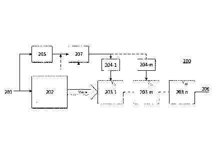
m, a
voltage booster power supply module 105 and a ground end 106. The power supply
module
102 and the n to-be-powered chips 103-n are sequentially connected in series
to the power
supply end 101 and the ground end 106. The power supply end 101 supplies a
power supply
voltage VCC to the circuit, and the ground end 106 supplies a ground GND for
the circuit.
The power supply module 102 output a voltage Vcore to supply series power to
the
1
Date Recue/Date Received 2020-12-16
CA 03104067 2020-12-16
to-be-powered chip 103-n. The m-th auxiliary power supply module 104-m
supplies power to
JO of the to-be-powered chips of the previous m stages. The auxiliary power
supply module
104-m can be directly powered by the power supply voltage VCC of the power
supply end
101, and also can supply the power supply voltage VCC after voltage boosting
of the voltage
booster power supply module 105 to the auxiliary power supply module 104-m.
[0007] Although the series power supply circuit 100 shown in FIG. 1 can
supply
series power to the to-be-powered chips, there are still deficiencies: (1)
when the power supply
voltage VCC directly powers the auxiliary power supply modules, and a voltage
difference
between the power supply voltage VCC and Vcore is small, the auxiliary power
supply modules
cannot work normally; (2) when the auxiliary power supply modules are powered
after voltage
boosting of the voltage booster power supply module, due to the requirement
for variable
frequency, Vcore is adjusted, when Vcore is decreased, the voltage difference
between the
voltage outputted from the voltage booster power supply module and Vcore gets
larger, and
may exceed a normal working voltage of the to-be-powered chips, such that the
auxiliary
power supply modules cannot work normally; (3) no matter whether the auxiliary
power
supply modules are directly powered by the power supply voltage VCC, or
powered after
voltage boosting of the voltage booster power supply module, when Vcore does
not exist, the
power supply voltage VCC or the voltage booster power supply module directly
powers 10
ends of the to-be-powered chips, causing the to-be-powered chips to be burnt
down.
SUMMARY OF THE INVENTION
[0008] To solve the above problems, the invention provides a voltage-
following
series power supply circuit, which can avoid the to-be-powered chips from
exceeding the
normal working voltage, even being burnt down, and also can decrease a power
supply
current, optimize power conversion efficiency, and reduce power consumption.
[0009] To realize the above object, the invention provides a voltage-
following series
power supply circuit, comprising:
[0010] a power supply end and a ground end;
2
Date Recue/Date Received 2020-12-16
CA 03104067 2020-12-16
100111 a power supply module comprising an input end connected to the power
supply end, and an output end for providing a power supply to two or more to-
be-powered
chips,
[0012] the power supply module and the to-be-powered chips connected in series
between the power supply end and the ground end; and
[0013] at least one auxiliary power supply module for supplying an
auxiliary power
supply to the to-be-powered chips,
[0014] wherein a voltage following module is further connected between the
power
supply end and the auxiliary power supply module for adjusting a voltage of
the auxiliary
power supply.
[0015] In the voltage-following series power supply circuit, the
voltage following
module adjusts the voltage of the auxiliary power supply according to a
voltage at the output
end of the power supply module.
[0016] In the voltage-following series power supply circuit, the
voltage at the output
end of the power supply module is configured to supply a reference voltage to
the voltage
following module.
[0017] In the voltage-following series power supply circuit, the
voltage following
module comprises a power supply input end, a ground input end, a power supply
output end,
a comparing amplifier unit, a sampling unit, a reference voltage generating
unit and a
switching unit.
[0018] In the voltage-following series power supply circuit, the power
supply input
end is connected to the power supply end, the ground input end is connected to
the output end
of the power supply module, and the power supply output end is connected to
the auxiliary
power supply module.
[0019] In the voltage-following series power supply circuit, the
switching unit is
connected to the power supply input end and the power supply output end, and
the comparing
amplifier unit controls the switching unit to turn on or turn off.
[0020] In the voltage-following series power supply circuit, the
sampling unit
comprises a first resistor and a second resistor connected in series; a first
end of the first
resistor is connected to the power supply output end, and a second end is
connected to a first
3
Date Recue/Date Received 2020-12-16
CA 03104067 2020-12-16
end of the second resistor; a second end of the second resistor is connected
to the ground input
end; the second end of the first resistor and the first end of the second
resistor are connected
to a positive input end of the comparing amplifier unit.
[0021] In the voltage-following series power supply circuit, the
reference voltage
generating unit is connected to the power supply input end and the ground
input end, and
supplies a reference voltage to a negative input end of the comparing
amplifier unit.
[0022] In the voltage-following series power supply circuit, the
switching unit
comprises a switching transistor.
[0023] In the voltage-following series power supply circuit, the
switching transistor
is a PMOS switching transistor.
[0024] In the voltage-following series power supply circuit, the
voltage following
module comprises standard LDO chips.
[0025] In the voltage-following series power supply circuit, it further
comprises a
voltage booster power supply module connected between the power supply end and
the
voltage following module.
[0026] To realize the above object, the invention further provides a
hash board for a
computing device, the hash board supplying a power supply using any of the
voltage-
following series power supply circuits.
[0027] To realize the above object, the invention further provides a
computing device,
comprising a power supply plate, a control board, a connection board, a
radiator and a plurality
of hash boards, the control board connected to the hash boards through the
connection board,
the radiator provided around the hash boards, the power supply plate for
supplying a power
supply to the connection board, the control board, the radiator and the hash
boards, wherein
the hash board is any of the hash boards.
[0028] The computing device can be configured to operation of mining
virtual digital
currency.
[0029] Application of the voltage-following series power supply circuit
of the
invention can avoid the possibility of the to-be-powered chips from exceeding
the normal
working voltage, even being burnt down, and also can decrease a power supply
current,
optimize power conversion efficiency, and reduce power consumption.
4
Date Recue/Date Received 2020-12-16
CA 03104067 2020-12-16
[0030] Hereinafter the invention is described in detail with reference
to the
accompanying drawings and the detailed embodiments, but the invention is not
limited
thereto.
BRIEF DESCRIPTION OF THE DRAWINGS
[0031] FIG. 1 is a schematic diagram of a current series power supply
circuit.
[0032] FIG. 2 is a schematic diagram of a voltage-following series
power supply
circuit according to the invention.
[0033] FIG. 3 is a circuit structural diagram of a voltage following
module according
to the invention.
[0034] FIG. 4 is a structural diagram of a hash board according to the
invention.
[0035] FIG. 5 is a structural diagram of a computing device according
to the
invention.
PREFERABLE EMBODIMENTS OF THE INVENTION
[0036] Hereinafter structure principle and working principle of the
invention are
described in detail with reference to the accompanying drawings.
[0037] Specific terms are used in the specification and the subsequent
claims to refer
to specific components. Those skilled in the art shall understand that the
manufacturer may
give a different name to the same component. The specification and the
subsequent claims
distinguish components from each other by different functions of the
components, instead of
different names. In the whole specification, the same reference sign
represents the same
element.
[0038] "Comprise" and "include" mentioned in the whole specification
and the
subsequent claims are open words, and shall be explained as "include but is
not limited to".
In addition, "connection" herein includes any direct or indirect electrical
connection means.
Indirect electrical connection means comprises connection through other
devices.
[0039] FIG. 2 is a schematic diagram of a voltage-following series
power supply
circuit according to the invention. As shown in FIG. 2, the voltage-following
series power
supply circuit 200 comprises a power supply end 201 and a ground end 206,
wherein the
Date Recue/Date Received 2020-12-16
CA 03104067 2020-12-16
power supply end 201 is connected to a system power supply VCC, and the ground
end 206
is connected to a system ground GND; a power supply module 202, comprising an
input end
connected to the power supply end 201, and an output end for providing a power
supply Vcore
to to-be-powered chips, wherein the to-be-powered chips 203-1...203-n are
plural, such as, n,
where n is a positive integer greater than 1. The to-be-powered chips 203-
1...203-n are
connected in series, wherein a power supply of the 1st stage to-be-powered
chip 203-1 is
connected to the output end of the power supply module 202, the ground end of
the 1st stage
to-be-powered chip 203-1 is connected to a power supply of the next-stage to-
be-powered
chip 203-2, and so on. A power supply of the to-be-powered chip of the present
stage is ground
of the preceding-stage to-be-powered chip, and the ground of the to-be-powered
chip of the
present is a power supply of the next-stage to-be-powered chip The ground of
the to-be-
powered chip 203-n of the final stage is connected to the ground end 206. It
shall be noted
that in the invention, the to-be-powered chips 203-1...203-n can be single
data processing
chips, and also can be a chip ground formed by connecting a plurality of data
processing chips
in parallel, but the invention is not limited thereto.
[0040] The voltage-following series power supply circuit 200 further
comprises a
plurality of auxiliary power supply modules 204-1...204-m, such as, m, where 1
--_,m n, and
m is a positive integer. The auxiliary power supply modules 204-1...204-m
supply power to
JO ends of the to-be-powered chips 203-1...203-n of the preceding m stages.
[0041] Generally, for example, a working voltage of the to-be-powered
chips
203-1...203-n can be 0.4V, and a working voltage of the auxiliary power supply
modules
204-1...204-m is 1.8V. When a voltage at the output end of the power supply
module 202 is
Vcore, a power supply voltage of the to-be-powered chip 203-1 is Vcore, and a
ground voltage
is Vcore-0.4; the power supply voltage of the m-th stage to-be-powered chip is
Vcore-0.4*(m-1),
and the ground voltage is Vcore-0.4*m.
[0042] To ensure the auxiliary power supply modules 204-1...204-m to
work
normally, the power supply voltage of the auxiliary power supply modules 204-
1...204-m
shall be at least the ground voltage of the to-be-powered chips 203-1...203-n
and the working
voltage 1.8V of the auxiliary power supply modules, i.e., Vcore-
0.4+1.8...Vcore-0.4*m+1.8.
6
Date Recue/Date Received 2020-12-16
CA 03104067 2020-12-16
[0043] Considering that internal resistances of the to-be-powered chips
of respective
stages are different, and in order to ensure the auxiliary power supply
modules to work
normally, the system power supply VCC often powers the auxiliary power supply
modules
after voltage boosting. Taking Vcore=10V and m=5 for example, the system power
VCC often
powers the auxiliary power supply modules after a voltage booster power supply
module 205
boosts the voltage to 14V. Accordingly, a voltage at both ends of the m-th
stage auxiliary
power supply module 204-m is 14- ( 10-0.4*5 ) =6V, and after subtracting a
working voltage
1.8V of the auxiliary power supply module 204-m, the voltage at both ends of
the auxiliary
power supply module 204-m is still higher than the voltage at normal working
by 6-1.8=4.2V.
[0044] When the to-be-powered chips are tuned, the voltage at the
output end of the
power supply module 202 shall be adjusted, for example, adjusting the voltage
Vcore to 8V.
Accordingly, the voltage at both ends of the m-th stage auxiliary power supply
module 204-m
is 14- ( 8-0.4*5) =8V, and after subtracting the working voltage 1.8V of the
auxiliary power
supply module 204-m, the voltage at both ends of the auxiliary power supply
module 204-m
is increased to 8-1.8=6.2V higher than the voltage at normal working.
Accordingly, the
voltage may exceed a safe working voltage of the auxiliary power supply module
204-m, even
the to-be-powered chip 203-m, causing the chip to be burned down.
[0045] Based on the foregoing reasons, the voltage-following series
power supply
circuit 200 of the invention adds a voltage follower module 207 between the
voltage booster
power supply module 205 and the auxiliary power supply modules 204-1...204-m.
[0046] FIG. 3 is a circuit structural diagram of a voltage following
module according
to the invention. Referring to FIGS. 3 and 2, the voltage follower module 207
comprises a
power input end 301, a switching unit 302, a comparing amplifier unit 303, a
reference voltage
generating unit 304, a ground input end 305, a sampling unit 306 and a power
output end 307.
The power input end 301 is connected to the power end 201 of the voltage-
following series
power supply circuit 200, or connected to an output end of the voltage booster
power supply
module 205. The ground input end 305 is connected to an input end of the power
supply
module 202, such that a voltage of the power output end 307 varies along with
the voltage
Vcore at the output end of the power supply module 202, and a difference
between the voltage
7
Date Recue/Date Received 2020-12-16
CA 03104067 2020-12-16
of the power output end 307 and the voltage Veore keeps constant, thereby
ensuring the voltage
at both ends of the auxiliary power supply modules 204-1...204-m to be always
within a range
of the safe working voltage.
[0047] The switching unit 302 is connected between the power input end
301 and the
power output end 307, and is controlled to turn on or turn off by an output
end of the
comparing amplifier unit 303. The switching unit 302 can be a PMOS transistor.
A source
electrode of the PMOS transistor is connected to the power input end 301, a
drain electrode is
connected to the power output end 307, and a gate electrode is connected to
the output end of
the comparing amplifier unit 303.
[0048] The comparing amplifier unit 303 can be an operational amplifier
with a power
supply connected to the power input end 301, and ground connected to the
ground input end
305. According to the safe working voltages of the auxiliary power supply
modules
204-1...204-m and/or the to-be-powered chips 203-1...203-n, a voltage value of
a reference
voltage Vref generated by the reference voltage generating unit 304 is set,
and the reference
voltage Vref generated by the reference voltage generating unit 304 serves as
a negative input
end of the comparing amplifier unit 303.
[0049] The sampling unit 306 is connected between the power output end 307 and
the
ground input end 305, and can be two resistors R. and Rh connected in series.
One end of the
resistor R. is connected to the power output end 307, and the other end is
connected to one
end of the resistor Rb. The other end of the resistor Rh is connected to the
ground input end
305. The other end of the resistor R. and one end of the resistor Rh are
connected to a positive
input end of the comparing amplifier unit 303.
[0050] Assuming that an output voltage of the power output end 307 is
\Tour, a voltage
at the positive input end of the comparing amplifier unit 303 is (Vour-
Veore)*Rb/(Ra+Rb), and
when (Vour-Veore)*Rb/(R.+Rb) < Vref, an output of the comparing amplifier unit
303 is "0".
Accordingly, the switching unit 302 is turned on to connect the power input
end 301 and the
power output end 307, the power output end 307 charges a load capacitor, and
the output
voltage \Tour of the power output end 307 is increased. When the voltage of
the power output
end 307 is increased to (Vour-Veore)*Rb/(R.+Rb)> Vref, the ouput of the
comparing amplifier
8
Date Recue/Date Received 2020-12-16
CA 03104067 2020-12-16
unit 303 is "1", the switching unit 302 is turned off, and the load capacitor
of the power output
end 307 discharges, such that the voltage of the power output end 307 is
decreased. Therefore,
(Vouf-Vcore)*RIARa+Rb) can be equal to Vref, i.e., Vout¨Vcore+Vref*( 1
+RaiRb). In other words,
the voltage of the power output end 307 of the voltage following module 207
varies along
with the voltage Vcore at the output end of the power supply module 202,
thereby ensuring that
the auxiliary power supply modules 204-1...204-m and the to-be-powered chips
203-1...203-n always work within the range of the safe working voltage.
[0051] The voltage following module of the invention can be separately
encapsulated
using the circuit structure of the voltage following module shown in FIG. 3,
and also can be
encapsulated together with other circuits.
[0052] The invention further provides a hash board, and FIG. 4 is a
structural diagram
of a hash board according to the invention. As shown in FIG. 4, each of the
hash boards 400
comprises one or more voltage-following series power supply circuits 200 to
perform hash
operation on working data sent downstream from a mining pool.
[0053] The invention further provides a computing device, and the
computing device
is preferably configured to operation of mining virtual digital currency. Of
course, the
computing device also can be configured to any other massive operations, and
FIG. 5 is a
schematic diagram of a computing device according to the invention. As shown
in FIG. 5,
each of the computing devices 500 comprises a connection board 501, a control
board 502, a
radiator 503, a power supply plate 504 and one or more hash boards 400. The
control board
502 is connected to the hash boards 400 through the connection board 501, and
the radiator
503 is provided around the hash boards 400. The power supply plate 504 is
configured for
supplying a power supply to the connection board 501, the control board 502,
the radiator 503
and the hash boards 400.
[0054] It shall be noted that in the invention, orientation or
positional relationship
indicated by the terms "transverse", "longitudinal", "up", "down", "front",
"back", "left",
"right", "vertical", "horizontal", "top", "bottom", "in", "out", and the like
is the orientation or
positional relationship illustrated by the drawings, and is only for the
purpose of describing
the invention and simplifying the explanation, rather than indicating or
suggesting that the
9
Date Recue/Date Received 2020-12-16
CA 03104067 2020-12-16
referred device or element must have specific orientation, and be constructed
and operated in
specific orientation, so it shall not be understood as limits to the
invention.
[0055] Although the embodiments of the invention have been disclosed above,
they
can be fully applied to various fields suitable for the invention but not as
limits to those listed
in the specification and the embodiments. For those skilled in the art,
additional modifications
can be easily implemented, so without departing from general concepts defined
by the
appended claims and equivalent scopes, the invention is not limited to
specific details and
figures illustrated and described here.
[0056] In other words, the invention also may have various other
embodiments, and
those skilled in the art shall make various corresponding modifications and
variations
according to the invention without departing from spirit and essence of the
invention, but these
corresponding modifications and variations shall belong to the scope protected
by the
appended claims of the invention.
Industrial Applicability
po571 Application of the voltage-following series power supply circuit
and the hash
board and the computing device applied thereto of the invention has the
following
advantageous effects:
[0058] capable of avoiding the possibility of the to-be-powered chips
from exceeding
the normal working voltage, even being burnt down, decreasing a power supply
current,
optimizing power conversion efficiency, and reducing power consumption.
Date Recue/Date Received 2020-12-16