Note: Descriptions are shown in the official language in which they were submitted.
A8140889CADIV
LIGHTING SYSTEM AND METHOD THEREOF
FIELD OF THE DISCLOSURE
The present disclosure relates generally to a lighting system and method, and
in
particular to a system, method, and related devices for controlling lights in
a plurality of rooms.
BACKGROUND
Lighting systems are known. The simplest lighting system may comprise a
plurality
of lighting devices such as incandescent lights, Compact Fluorescent Lamps
(CFLs), Light-
Emitting Diodes (LEDs), and the like, distributed in a site such as a building
with a plurality
of rooms. The lighting devices may be powered by a power source such as an
Alternate
Current (AC) grid. A plurality of light switches may be installed in the rooms
and each coupled
to one or more lighting devices for controlling the on/off of the
corresponding lighting devices.
More sophisticated lighting systems have also been developed. For example, US
Patent No. 10/194,507B2 to Snyder teaches a system, method, and apparatus for
powering
intelligent lighting networks. The power for the intelligent lighting network
is supplied by
Power-over-Ethernet (PoE) switches and/or Mid-Spans, which are conditioned by
a powered
device to distribute power tuned specifically for each, at least one LED
fixture. The PoE
switch and/or Mid-Span with associated router and wireless access point is
used to
communicate with and power a sensor network that collects data relevant to the
intelligent
1
Date Recue/Date Received 2021-01-18
A8140889CADIV
lighting network. Optionally, the PoE switch and/or Mid-Span is used to
communicate with
and power a network of sensors that collects data relevant to the space the
intelligent lighting
network is operating in or is used to communicate with and power a network of
AC wall plugs
that is turned on and off and various switches, relays, PLCs, RFID systems,
USB hubs, etc.
US Patent Application Publication No. 2017/0147018A1 to Meruva, et al. teaches
an
automatic master-slave system and approach for coordinated control of a
parameter, for
example, a heating, ventilation and air conditioning condition, in an area of
multiple spaces
controlled by room controllers. Changing a layout of a zone/area in a building
such as moving,
adding or removing a door, increasing or splitting size of a room through
movable walls, or
by permanently removing partitions, changing offices to a conference room or
vice versa, may
occur. A size of a room may be altered within minutes, according to customer
demand. For
instance, rooms may be converted into a single room by removing partitions.
The controllers
that were controlling temperatures of the rooms independently earlier, may
convert
automatically into a master-slave configuration and now work together to
control a larger
room. If the large room is split into multiple rooms, the controllers may
automatically revert
to their previous configuration.
US Patent No. 8,583,843B2 to Rosso teaches a communications control bus and
apparatus for controlling multiple electronic hardware devices. The bus
comprises an IMB
slave CPU, at least two registers, and a three-bit data connector, which
connects the two
registers. The connector permits transmission of a three-bit data signal
between the two
registers. A network interconnects the two registers and the IMB slave CPU.
2
Date Recue/Date Received 2021-01-18
A8140889CADIV
US Patent Application Publication No. 2018/0335870A1 to Ali, et al. teaches
system,
method, and computer-program product embodiments that can support touch
interaction on a
projective capacitive (PCAP) display system in the presence of water
contamination.
According to an embodiment, a system includes a touchscreen coupled to a
controller. The
controller determines the presence of water contamination on the touchscreen,
and obtains
measurements during a mixed-mode measurement frame that includes a self-mode
measurement and a mutual-mode measurement. Based on the measurements obtained,
the
controller determines a touch on the touchscreen in the presence of the water
contamination
on the touchscreen. In some embodiments, the self-mode measurement includes
measurements collected at a both lower and a higher drive frequency, the
higher drive
frequency may be in the frequency range of 100 kHz to 500 kHz. In another
embodiment, the
self-mode measurement includes simultaneously measuring both horizontal-
electrodes and
vertical-electrodes.
US Patent Application Publication No. 2019/0120471A1 to Witty, et al. teaches
multi-
function wall switches. A wall switch can include a master assembly and daisy-
chained slave
assemblies. The master assembly can include more components than the slave
assemblies to
implement more functionality in a single assembly.
A lighting system generally requires a variety of devices. For example,
lighting control
devices such as wall-mount switches and dimmers have been widely used.
However, existing
lighting control devices have drawbacks. For example, installation of existing
lighting control
devices for mid to large size professional/commercial sites is generally
expensive, involves
complicated and user-/installer-unfriendly installation processes, and
requires a proprietary
wiring architecture. Large bulky control interfaces require special or
customized electrical
3
Date Recue/Date Received 2021-01-18
A8140889CADIV
back boxes. Communication protocols are often proprietary and outdated, and
require
communication back to one or more central processing systems of various types.
LED dimmers are also known. Existing LED dimmers designed for line voltage
dimming such as those for used at about 120 VAC in North America are typically
inexpensive
and can be mass-produced. However, existing LED dimmers are often of poor
quality and are
generally designed for low-wattage (e.g., less than 180W) residential or
commercial single-
circuit manual-control.
Almost all existing line-voltage LED dimmers specify the various LED lamps
they are
designed to be used with for optimum performance (read: to minimize "pop on",
"flicker",
"dead zones", "false triggering", etc.) vice versa for the LED lamps
manufacturers. However,
they typically specify the preferred dimmer.
Hitherto, it appears that there are no manufacturers addressing the industry
requirement of a professional-grade high-density dimmer system (multi-channel)
designed for
various self-ballasted LED load types operating at line voltage, and no
manufacturer to date
has produced an LED dimmer that can "play nice" with virtually any of the
various type of
LED lamps offering reliable performance and a stable full range of dimming
without the
typical associated problems.
Electronic Theatre Controls Inc. of Middleton, Wisconsin, U.S.A. makes a rack
LED
dimmer as an option to their bussed relay rack system. However, it is
relatively unintelligent
and limited to a maximum of 300W.
4
Date Recue/Date Received 2021-01-18
A8140889CADIV
Therefore, there is always a desire for a lighting system with low cost, ease
of
installation, and ease of control.
SUMMARY
According to one aspect of this disclosure, there is provided a lighting
system for
deploying in a lighting area, the light area comprising a plurality of
lighting subareas. The
lighting system comprises: a plurality of central-control devices electrically
connected in a
first daisy-chain form; and a plurality of groups of local light-control
devices for deploying in
the plurality of lighting subareas for controlling a plurality of lighting
devices therein. Each
group of local light-control devices are electrically connected in a second
daisy-chain form;
and each group of local light-control devices are connected to one of the
plurality of central-
control devices.
In some embodiments, the plurality of central-control devices and the
plurality of
groups of local light-control devices form a distributed lighting control
structure.
In some embodiments, a first one of the plurality of central-control devices
of the first
daisy-chain is automatically configured as a master central-control device,
and others of the
plurality of central-control devices of the first daisy-chain are configured
as slave central-
control devices manageable by the master central-control device.
In some embodiments, each central-control device comprises a plurality of
input ports
each configured for connecting one of the plurality of groups of local light-
control devices.
5
Date Recue/Date Received 2021-01-18
A8140889CADIV
In some embodiments, one of the plurality of input ports is configured for
connecting
to a next one of the plurality of central-control devices in the first daisy-
chain.
In some embodiments, each central-control device further comprises an output
port
for connecting to a previous one of the plurality of central-control devices
in the first daisy-
chain.
In some embodiments, each central-control device is configured for maintaining
a link
table recording a mapping between the plurality of groups of local light-
control devices and
the plurality of lighting subareas.
In some embodiments, each group of local light-control devices control one or
more
.. of the plurality of lighting devices in one of the plurality of lighting
areas.
In some embodiments, in each second daisy-chain, a first one of the plurality
of local
light-control devices is automatically configured as a master local light-
control device, and
others of the plurality of local light-control devices are configured as slave
local light-control
devices manageable by the master local light-control device.
In some embodiments, each of the plurality of local light-control devices
comprises a
touch-sensitive screen.
In some embodiments, the touch-sensitive screen is configured for displaying a
plurality of touchable icons for triggering a plurality of functions.
In some embodiments, the plurality of touchable icons comprise a clean-screen
icon
.. for disabling the touch response of the touch-sensitive screen for a
predefined time-period.
6
Date Recue/Date Received 2021-01-18
A8140889CADIV
In some embodiments, each of the plurality of local light-control devices
comprises a
motion sensor and a light sensor.
In some embodiments, each of the plurality of local light-control devices
comprises a
faceplate; and wherein the faceplate comprises a pair of tubes engageable with
the motion
sensor and the light sensor, respectively, for preventing ambient light from
entering the light
sensor and the motion sensor.
According to one aspect of this disclosure, there is provided an electrical
device for
mounting to an anchor, the electrical device comprising: a faceplate having a
front wall and a
sidewall, the front wall and the sidewall forming a recess, the faceplate
comprising one or
more rearward extending screw-holes on the front wall for receiving one or
more screws, and
comprising one or more clips on the sidewall; a circuitry received in the
recess, the circuitry
comprising one or more first openings at locations corresponding to those of
the one or more
rearward extending screw-holes of the faceplate for the one or more screws to
extend
therethrough, and comprising one or more second openings on one or more edges
thereof at
locations corresponding to those of the one or more clips of the faceplate for
the one or more
clips to extend therethrough; and a mounting plate for mounting to an anchor,
the mount plate
comprising one or more recesses on one or more edges thereof for engaging the
one or more
clips of the faceplate so as to engage the faceplate and sandwich the
circuitry therebetween,
and comprising one or more recesses at locations corresponding to those of the
one or more
rearward extending screw-holes of the faceplate for receiving therein heads of
the one or more
screws so as to reduce the thickness of the electrical device.
7
Date Recue/Date Received 2021-01-18
A8140889CADIV
In some embodiments, the mounting plate has a dimension for mounting to a
single-
gang electrical box.
In some embodiments, the circuitry comprises a touch-sensitive screen; and
wherein
the front wall of the faceplate comprises an opening for receiving the touch-
sensitive screen.
In some embodiments, the circuitry comprises at least one printed circuit
board (PCB).
In some embodiments, the circuitry comprises at least two PCBs mechanically
and
electrically coupled together; and the electrical device further comprises at
least one PCB
spacer sandwiched between the at least two PCBs for supporting the at least
two PCBs.
In some embodiments, the touch-sensitive screen is mechanically and
electrically
couple to a front one of the at least two PCBs.
In some embodiments, the circuitry comprises a motion sensor and a light
sensor.
In some embodiments, the front PCB comprises a motion sensor and a light
sensor.
In some embodiments, the faceplate comprises a pair of tubes engageable with
the
motion sensor and the light sensor, respectively, for preventing ambient light
from entering
the light sensor and the motion sensor.
In some embodiments, a rear one of the at least two PCBs has a dimension
smaller
than a front one of the at least two PCBs.
In some embodiments, a rear one of the at least one PCB spacer supports the
rear PCB;
and wherein the rear PCB spacer has a dimension same as that of the rear PCB.
8
Date Recue/Date Received 2021-01-18
A8140889CADIV
In some embodiments, rear PCB comprises at least one of one or more RJ-45
connectors, a plurality of dual in-line package (DIP) switches, and a
plurality of breakaway
terminal block connectors.
In some embodiments, the electrical device further comprises a cover for
engaging the
faceplate and sandwiching the circuitry therebetween, the cover comprising one
or more first
openings at locations corresponding to those of the one or more rearward
extending screw-
holes of the faceplate for the one or more screws to extend therethrough, and
comprising one
or more second openings on one or more edges thereof at locations
corresponding to those of
the one or more clips of the faceplate for the one or more clips to extend
therethrough.
In some embodiments, the cover further comprises a third opening have a
rearward-
extending sidewall thereabout, the third opening having a dimension same as
that of the rear
PCB for the rear PCB to extend therethrough, and the sidewall of the cover
having a height
flush with the rear PCB.
According to one aspect of this disclosure, there is provided an electrical
device
comprising: a plurality of stacked electrical circuit boards; a plurality of
spacers, each of said
spacers is configured between a pair of neighboring electrical circuit boards
for separation and
support thereof; an enclosure comprising perimetric sidewalls and a plurality
of perimetric
grooves on an inner side of the sidewalls, each of the groove receiving
therein a respective
electrical circuit board.
In some embodiments, the enclosure has a dimension for sitting into a single-
gang
electrical box.
9
Date Recue/Date Received 2021-01-18
A8140889CADIV
In some embodiments, the enclosure comprises a pair of enclosure halves.
In some embodiments, a top electrical circuit board of the plurality of
stacked electrical
circuit boards comprises a touch-sensitive display coupled thereto, and
wherein the enclosure
comprises a perimetric step for receiving the touch-sensitive display thereon.
According to one aspect of this disclosure, there is provided an electrical
device
comprising: a circuit board; an insert having at least a front frame, two side-
frames, and a rear
wall having two opposite ends, said insert comprising one or more protrusions
perimetrically
distributed on outer side surfaces of said front and side frames, said rear
wall comprising a
ridge, said ridge and the front and side frames forming a supporting
structure; and a housing
structure having at least a front wall and two sidewalls, each of said
sidewall comprising a
groove for receiving a respective end of the rear wall of the insert, said
housing structure
comprising one or more recesses perimetrically distributed on inner surfaces
of said front and
sidewalls for receiving the one or more protrusions, and said housing
structure comprising a
shoulder on an inner side thereof and across said front wall and sidewalls,
said should facing
said recesses and collaborating with the supporting structure of the insert
for sandwiching said
circuit board therebetween.
BRIEF DESCRIPTION OF THE DRAWINGS
FIG. 1 is a schematic diagram showing a lighting system according to some
embodiments of this disclosure, wherein the lighting system comprising a
plurality of local
light-control devices controlling a plurality of lights in a site and a light-
control center having
Date Recue/Date Received 2021-01-18
A8140889CADIV
one or more central-control devices and connected to the local light-control
devices for
controlling the local light-control devices and in the lights connected
thereto;
FIGs. 2A and 2B are perspective views of the central-control device of the
light-
control center of the lighting system shown in FIG. 1, viewing from different
viewing angles;
FIG. 2C is a perspective view of the central-control device shown in FIG. 2A
with the
top cover removed for showing the components therein;
FIG. 3 is a front view of a navigation structure of the central-control device
shown in
FIG. 2A;
FIG. 4 is a schematic diagram showing the electrical connections between the
central-
control devices and the local light-control devices;
FIG. 5 is a schematic diagram showing the electrical connections between the
central-
control devices and the local light-control devices in an exemplary
embodiment;
FIGs. 6A and 6B are perspective views of a local light-control device of
lighting
system shown in FIG. 1, view from different viewing angles;
FIG. 6C is a front view of the local light-control device shown in FIG. 6A;
FIG. 6D is a rear view of the local light-control device shown in FIG. 6A;
FIG. 7A is a perspective view of the local light-control device shown in FIG.
6A
attached to a single-gang electrical box on a wall;
11
Date Recue/Date Received 2021-01-18
A8140889CADIV
FIG. 7B is a side view of the local light-control device shown in FIG. 6A
attached to
a single-gang electrical box on a wall;
FIGs. 8A and 8B are exploded perspective views of the local light-control
device
shown in FIG. 6A, viewed from different viewing angles, wherein the local
light-control
device comprises a faceplate, a circuitry, a PCB spacer, a rear cover, and a
wall-plate;
FIGs. 9A and 9B are perspective views of the faceplate of the local light-
control device
shown in FIG. 6A, viewed from different viewing angles;
FIGs. 9C and 9D are front a rear views of the faceplate of the local light-
control device
shown in FIG. 6A;
FIGs. 9E and 9F are side views of the faceplate of the local light-control
device shown
in FIG. 6A;
FIGs. 9G and 9H are plan view and bottom view, respectively, of the faceplate
of the
local light-control device shown in FIG. 6A;
FIG. 10A is a perspective view of the circuitry of the local light-control
device shown
in FIG. 6A;
FIG. 10B is a side view of the circuitry of the local light-control device
shown in
FIG. 6A;
FIG. 10C is a rear view of the circuitry of the local light-control device
shown in
FIG. 6A;
12
Date Recue/Date Received 2021-01-18
A8140889CADIV
FIGs. 11A and 11B are perspective views of the rear cover of the local light-
control
device shown in FIG. 6A, viewed from different viewing angles;
FIGs. 12A and 12B are perspective views of the wall-plate of the local light-
control
device shown in FIG. 6A, viewed from different viewing angles;
FIG. 13A is a screenshot of a touchscreen of the local light-control device
shown in
FIG. 6A, wherein the touchscreen may display a plurality of icons for
performing various
functions;
FIG. 13B is a screenshot of a touchscreen of the local light-control device
shown in
FIG. 6A, wherein the touchscreen displays a diagram for a "SYNC" function;
FIGs. 14A is a perspective view of a LED controller viewed from a front side
thereof,
according to some embodiments of this disclosure, wherein the electrical
device comprises an
enclosure and an electrical assembly;
FIG. 14B is a perspective view of the LED controller shown in FIG. 14A viewed
from
a rear side thereof;
FIG. 14C is a plane view of the LED controller shown in FIG. 14A;
FIG. 15 is a perspective view of an enclosure half of the enclosure of the LED
controller shown in FIG. 14A, viewing from the front side thereof;
FIG. 16 is a plan view of the enclosure half shown in FIG. 15, viewed from the
front
side thereof;
13
Date Recue/Date Received 2021-01-18
A8140889CADIV
FIG. 17 is a rear view of the enclosure half shown in FIG. 15, viewed from the
rear
side thereof;
FIGs. 18 to 21 are side views of the enclosure half shown in FIG. 15, viewed
from
different sides thereof;
FIG. 22A is a cross-sectional view of the enclosure half shown in FIG. 15
along the
cross-sectional line A-A shown in FIG. 16;
FIG. 22B is a cross-sectional view of the enclosure half shown in FIG. 15
along the
cross-sectional line B-B shown in FIG. 16;
FIG. 22C is a cross-sectional view of the enclosure half shown in FIG. 15
along the
cross-sectional line C-C shown in FIG. 16;
FIG. 23 is a bottom view of a mounting bracket for mounting two enclosure
halves
shown in FIG. 15 to form the enclosure of the LED controller shown in FIG.
14A;
FIG. 24 is a perspective view of the mounting bracket shown in FIG. 23;
FIG. 25A is a lateral-side view of the enclosure of the LED controller shown
in FIG.
14A, viewing from the front side thereof;
FIG. 25B is a plan view of the enclosure of the LED controller shown in FIG.
14A,
viewing from the front side thereof;
FIG. 26 is a perspective view of the electrical assembly of the LED controller
shown
in FIG. 14A, viewing from the front side thereof;
14
Date Recue/Date Received 2021-01-18
A8140889CADIV
FIG. 27 is a plan view of a touch-sensitive display of the electrical assembly
shown in
FIG. 26A;
FIGs. 28 and 29 are side views of the touch-sensitive display shown in FIG.
27;
FIG. 30A is a perspective view of the touch-sensitive display shown in FIG. 27
mounted on a first side of a first electrical circuit board of the electrical
assembly shown in
FIG. 26A;
FIG. 30B is a perspective view of the touch-sensitive display and the
electrical circuit
board shown in FIG. 30A;
FIGs. 31 and 32 are schematic plan views of a first and a second side of a
second PCB
of the electrical assembly shown in FIG. 26A;
FIGs. 33 and 34 are schematic plan views of a first side and a second side of
a third
PCB of the electrical assembly shown in FIG. 26A;
FIG. 35 is a cross-sectional view of the LED controller shown in FIG. 14A
along the
cross-sectional line X-X shown in FIG. 14C;
FIGs. 36 to 38 are perspective views of an electrical device from various
viewing
directions, according to some embodiments of this disclosure, wherein the
electrical device
comprises an enclosure and an electrical circuit board;
FIG. 39 is an exploded view of the electrical device shown in FIG. 36;
FIG. 40 is a perspective view of a housing structure of the enclosure of the
electrical
device shown in FIG. 36, viewing from a bottom side of the housing structure;
Date Recue/Date Received 2021-01-18
A8140889CADIV
FIGs. 41 is a perspective view of the housing structure of the enclosure of
the electrical
device shown in FIG. 36, viewing from a top side of the housing structure;
FIG. 42 is a plan view of the housing structure shown in FIG. 40;
FIG. 43 is a bottom view of the housing structure shown in FIG. 40;
FIG. 44 is a front view of the housing structure shown in FIG. 40;
FIG. 45 is a rear view of the housing structure shown in FIG. 40;
FIG. 46 is a cross-sectional view of the housing structure shown in FIG. 40
along the
sectional line A-A shown in FIG. 43;
FIGs. 47 and 48 are perspective views of an insert of the enclosure of the
electrical
device shown in FIG. 36, viewing from a bottom side of the insert;
FIG. 49 is a plan view of the insert shown in FIG. 47;
FIG. 50 is a bottom view of the insert shown in FIG. 47;
FIG. 51 is a side view of the insert shown in FIG. 47;
FIG. 52 is a front view of the insert shown in FIG. 47;
FIG. 53 is a rear view of the insert shown in FIG. 47;
FIG. 54 is a plan view of an assembled enclosure of the electrical device
shown in
FIG. 36;
16
Date Recue/Date Received 2021-01-18
A8140889CADIV
FIG. 55 is a cross-sectional view of the assembled enclosure of the electrical
device
shown in FIG. 36 along the sectional line B-B shown in FIG. 54;
FIGs. 56 and 57 are perspective views of a button of the electrical device
shown in
FIG. 36;
FIG. 58 is a plan view of the button shown in FIG. 56;
FIG. 59 is a bottom view of the button shown in FIG. 56;
FIG. 60 is a side view of the button shown in FIG. 56;
FIG. 61 is a front view of the button shown in FIG. 56;
FIG. 62 is a rear view of the button shown in FIG. 56;
FIG. 63 is a cross-sectional view of the button shown in FIG. 56 along the
sectional
line C-C shown in FIG. 59;
FIG. 64 is a schematic plan view of an electrical circuit board of the
electrical device
shown in FIG. 36;
FIGs. 65 to 67B illustrate a process of assembling the electrical device shown
in
FIG. 36, wherein
FIG. 65 shows positioning the pushbutton (shown in FIGs. 56 to 63) into the
housing
structure (shown in FIGs. 40 to 46),
FIGs. 66A and 66B show positioning the PCB (shown in FIG. 64) onto the insert
(shown in FIGs. 47 to 53), and
17
Date Recue/Date Received 2021-01-18
A8140889CADIV
FIGs. 67A and 67B show inserting the assembled PCB and insert (shown in FIGs.
66A
and 66B) into the housing structure (shown in FIG. 65); and
FIGs. 68 and 69 are perspective views of an expandable circuit board having a
plurality
of the electrical device shown in FIG. 36.
DETAILED DESCRIPTION
In the following embodiments of an electrical device are described. In the
description,
directional phrases such as "top", "bottom", "up", "down", "front", "rear",
"left" and "right"
are used only for describing the directions of components relative to each
other.
Turning now to FIG. 1, a lighting system is shown and is generally identified
using
reference numeral 100. As shown, the lighting system 100 is deployed in a site
102 such as a
building having a plurality of subareas such as a plurality of rooms and/or
zones.
In these embodiments, the lighting system 100 comprises a plurality of local
light-
control devices 106 such as a plurality of wall-mount control stations
controlling a plurality
of lights 104 distributed in the subareas of the site 102. Each subarea
comprises one or more
local light-control devices 106 and each local light-control device 106
controls one or more
lights 104 in the subarea via one or more LED dimmers (not shown).
The lighting system 100 further comprises a light-control center 108 connected
to the
local light-control devices 106 for controlling the local light-control
devices 106 and in turn
controlling the lights 104.
18
Date Recue/Date Received 2021-01-18
A8140889CADIV
The light-control center 108 in these embodiments comprises a plurality of
central-
control devices 122 linked or otherwise electrically connected for controlling
the lights 104
via the local light-control devices 106.
FIGs. 2A and 2B show an example of a central-control device 122 such as
Applicant's
PRESIDOR room linker/combiner (PRESIDOR is a registered trademark of Johnson
Systems Inc. of Bragg Creek, Alberta, Canada, the Applicant of the subject
application).
FIG. 2C is a perspective view of the central-control device 122 with the top
cover removed
for showing the electrical circuitry therein.
As shown, the central-control device 122 in these embodiments comprises a
housing 124 with a pair of mounting brackets 126 coupled on opposite sides
thereof for
attaching the central-control device 122 to an anchor such as a wall, a rack,
or the like.
The housing receives therein an electrical circuitry 128 having a printed
circuit board
(PCB) with a plurality of electrical components thereon. On the front side of
the housing 124,
the central-control device 122 comprises a display 130 and a navigation
structure 132
electrically connected to the circuitry. The display 130 is used for
displaying configuration
information and a menu system for adjusting the configuration settings.
As shown in FIG. 3, the navigation structure 132 is arranged in a circular
shape with
a selection button 134 at the center thereof surrounded by four arrow buttons
136 to 142. The
selection button 134 is used for triggering the display of the menu system on
the display 130
and for making a selection of a configuration setting. The up and down buttons
136 and 138
are used for cycling the menu items of the menu system on the display 130,
wherein each
menu item may correspond to a configuration item and comprise a plurality of
configuration
19
Date Recue/Date Received 2021-01-18
A8140889CADIV
options. The left and right buttons 140 and 142 are used for highlighting a
configuration
option. When a configuration option is highlighted, a user may press the
selection button 134
to select the highlighted option as the setting for the corresponding
configuration item. Some
menu items may comprise submenu items and pressing the selection button 134
may trigger
the display of the submenu items on the display 130.
Referring back to FIGs. 2B and 2C, on the rear side of the housing 124, the
central-
control device 122 comprises a power port 152 for receiving a power cord for
powering the
central-control device 122, a plurality of downlink ports 154 for connecting
the local light-
control devices 106, an interlink port 156 (also denoted a DMX Output (DO)
port) for
connecting or interlinking to another central-control device 122, a networking
port 158 for
connecting a computing device such as a laptop or a network
display/touchscreen to link the
rooms remotely, and a plurality of auxiliary ports 160. In these embodiments,
the downlink
ports 154 are RJ-45 ports and use the DMX512 standard protocol which is a
standard protocol
for digital communication networks that are commonly used to control stage
lighting and
effects. The interlink port 156 is a RJ-45 port using a suitable interlink
communication
protocol.
The auxiliary ports 160 are programmable contact closure inputs to permit a
plurality
of master local light-control devices 106 (described in more detail later) to
be "linked" as
configured in the central-control device 122 such that one may initiate some
operation
instructions (e.g., executing a lighting preset for some subareas at the
central-control device
122) to cause the linked master local light-control devices 106 to perform the
corresponding
operations.
Date Recue/Date Received 2021-01-18
A8140889CADIV
In some embodiments, an external dry-contact maintained switch may be used to
contact one of the auxiliary ports 160 with a common terminal which then
triggers the central-
control device 122 to link the master local light-control devices 106A
(described in more detail
later) as required in any matrix of combinations.
For example, if an auxiliary port 160 is programmed to link the master local
light-
control devices 106A in rooms #1, #4, #7, and #22, then, an operator may press
a button
(which may be a physical button or a digital button displayed on a touch-
sensitive screen),
such as a preset button, of a local light-control devices 106 in any of the
rooms #1, #4, #7, and
#22 to send a command to the linked rooms #1, #4, #7, and #22 to perform an
action (e.g., to
use a predefined set of parameters).
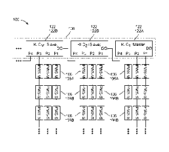
FIG. 4 is a schematic diagram of the lighting system 100 showing the
connections of
the light-control center 108 and the local light-control devices 106. The
light-control
center 108 comprises a plurality of interconnected central-control devices
122. For ease of
illustration, each central-control device 122 shown in FIG. 4 has four
downlink ports 154
denoted Pl, P2, P3, and P4, and one interlink port 156 denoted DO. In these
embodiments,
the downlink ports 154 are input ports and the interlink port or DO port 156
is an output port.
However, as will be described in more detail later, a dedicated one of the
downlink ports 154
such as P4 of a first central-control device may be connected to the DO port
156 of a second
central-control device, wherein the two central-control devices may
automatically the
connection therebetween and automatically convert the dedicated downlink ports
154 of the
first central-control device and the DO port 156 into bidirectional
communication ports.
21
Date Recue/Date Received 2021-01-18
A8140889CADIV
As shown in FIG. 4, the central-control devices 122 are interconnected in the
form of
a central-control daisy chain using RJ-45 cables (i.e., cables e.g. Cat5e or
Cat6 cables with
RJ-45 connectors). The first central-control device 122A at the beginning of
the central-
control daisy chain acts as a master central-control device and other central-
control devices
122B along the central-control daisy chain act as slave central-control
devices under the
control or management of the master central-control device 122A.
For ease of description, an interlink direction may be defined as a direction
from the
master device to the last device in the daisy chain. Correspondingly, the term
"upstream"
device refers to the master device or a slave device closer to the master
device compared to
another slave device, and the term "downstream" device refers to a slave
device further away
from the master device compared to another slave device. In other words, the
interlink
direction is a direction from an "upstream" device to a "downstream" device.
In these embodiments, an upstream central-control device 122 uses a dedicated
downlink port such as the downlink port P4 to connect to the interlink port
DO/156 of the
.. immediately downstream central-control device for forming the central-
control daisy chain.
Therefore, the dedicated downlink port may be used for connecting to local
light-control
devices 106 or a downstream central-control device 122 while other downlink
ports may only
be used for connecting to local light-control devices 106. The central-control
device 122
monitors the devices connected to the dedicated downlink port P4 and
automatically
determines how to communicate therewith.
In the example shown in FIG. 4, the master central-control device 122A
(denoted
RLCi in FIG. 4) is interconnected to the first slave central-control device
122B (denoted RLC2
22
Date Recue/Date Received 2021-01-18
A8140889CADIV
in FIG. 4) by connecting the downlink port P4 of the master central-control
device 122A to
the interlink port DO/156 of the first slave central-control device 122B.
Similarly, the n-th
(n = 1, 2, 3, ...) slave central-control device (denoted RLCn in FIG. 4) is
interconnected to
the (n+1)-th slave central-control device RLCn+1 by connecting the downlink
port P4 of the
n-th central-control device RLCn to the interlink port DO/156 of the (n+1)-th
slave central-
control device RLCn+1.
Except those used for central-control-device interconnections, each downlink
port 154
of the central-control devices 122A and 122B may be used for connecting one or
more local
light-control devices 106 arranged in the form of a local-control daisy chain.
In each local-
control daisy chain, the local light-control device 106A at the beginning
thereof acts as a
master local light-control device (denoted PWS-M in FIG. 4) and other local
light-control
devices 106B downstream thereto act as slave local light-control devices
(denoted PWS-S in
FIG. 4) under the control or management of the master local light-control
device 106A.
In these embodiments, the system 100 has four types of connections (FIG. 4
shows
three of them), wherein each type of connection may use a different
communication protocol
for data communication between the connected devices, including:
(1) connection between the central-control devices/RLCs 122 (e.g., the master
RLC
122A to the slave RLC 122B immediately connected thereto, or a slave RLC 122B
to another
slave RLC 122B immediately connected thereto): using a hybrid or modified
DMX512
protocol.
23
Date Recue/Date Received 2021-01-18
A8140889CADIV
(2) connection between a central-control device/RLC 122 and a master local
light-
control device/PWS-M 106A immediately connected thereto: using the hybrid or
modified
DMX512 protocol.
(3) connection between a local light-control device/PWS 106 (which may be a
master
local light-control device/PWS-M 106A or a slave local light-control
device/PWS-S 106B)
and another local light-control device/PWS 106 (which may be a slave local
light-control
device/PWS-S 106B): using a suitable bidirectional multiplex data
communication protocol
such as Applicant's Presidor Multiplexed data communication protocol (PMX).
(4) connection between the DO port 156 of a central-control device/RLC 122 and
a
device that is not a central-control device/RLC: using the standard DMX512
protocol.
In some embodiments, the DO port 156 may be used for connecting one or more
LED
dimmers using the standard DMX512 protocol, wherein each dimmer uses a DMX
channel.
In this manner, a central-control device/RLC 122 may directly control up to
512 LED dimmers
for controlling the lights 104 connected thereto.
In these embodiments, the central-control device/RLC 122 monitors the device
connected to the DO port 156 thereof and automatically determines the
communication
protocol to be used. In particular, if the central-control device/RLC 122
detects that the device
connected to the DO port 156 thereof is another central-control device/RLC
122', the central-
control device/RLC 122 then automatically uses the hybrid or modified DMX512
for
communication through the DO port 156; if the central-control device/RLC 122
detects that
the device connected to the DO port 156 thereof is not a central-control
device/RLC, the
24
Date Recue/Date Received 2021-01-18
A8140889CADIV
central-control device/RLC 122 then automatically uses the standard DMX512 for
communication through the DO port 156.
With the system topology shown in FIG. 4, each local-control daisy chain
allows any
local light-control device 106 thereof to control the lights 106 connected to
the local-control
daisy chain (via corresponding local light-control devices 106 in the daisy
chain). The central-
control devices 122 of the central-control daisy chain collaborate with each
other under the
management of the master central-control device 122A for room or subarea
linking such as
linking a plurality of local-control daisy chains together such that any local
light-control
device 106 of the linked local-control daisy chains may control the lights 106
connected to
the linked local-control daisy chain (via corresponding local light-control
devices 106). Such
a system design and topology enable a distributed lighting control.
In some embodiments, each master local light-control device 106A provides
settings
to allow a user such as an administrator or an authorized user to apply
lighting control
restrictions and/or user access-rights to the master local light-control
device 106A and the
slave local light-control devices 106B daisy-chained thereto.
FIG. 5 is a schematic diagram of a lighting system 100 in an exemplary
embodiment.
In this example, the light-control center 108 comprises two central-control
devices 122A
and 122B for controlling the local light-control devices 106 in five (5)
rooms. Each central-
control device 122A/122B comprises four (4) downlink ports P1 to P4 configured
as input
ports and an interlink port DO configured as an output port. The downlink port
P4 is the
dedicated port for interconnecting a downstream central-control device 122 or
for connecting
to one or more daisy-chained local light-control devices 106.
Date Recue/Date Received 2021-01-18
A8140889CADIV
In this example, the central-control device 122A is at the beginning of the
central-
control daisy chain and thus acts as the master central-control device. The
central-control
device 122B then acts as a slave central-control device. Accordingly, the
central-control
devices 122A and 122B are interconnected by connecting the input downlink-port
P4 of the
master central-control device 122A to the output interlink-port DO of the
slave central-control
device 122B via a RJ-45 cable 162. The master central-control device 122A is
in
communication with the slave central-control device 122B under a suitable
bidirectional data-
communication protocol such as a hybrid or modified DMX512 protocol.
The central-control daisy chain may be expanded by connecting additional slave
.. central-control devices to the slave central-control device 122B in series
using RJ-45 cables
in a similar manner (input downlink-port P4 of an upstream slave central-
control device 122B
connecting to the output interlink-port DO of a downstream slave central-
control
device 122B). When a downstream slave central-control device 122B is connected
to the
central-control daisy chain, the upstream and downstream central-control
device (being the
.. master central-control device 122A or a slave central-control device 122B)
and the
downstream central-control device 122B automatically detect the connection
therebetween
and automatically convert the dedicated downlink ports 154 of the first
central-control device
and the DO port 156 into bidirectional communication ports for communicating
bidirectional
data under the hybrid or modified DMX512 protocol. In this manner, a central-
control device
.. in a central-control daisy chain may communicate with other central-control
devices of the
central-control daisy chain and may communicate with the local light-control
devices 106 via
the central-control devices linked thereto.
26
Date Recue/Date Received 2021-01-18
A8140889CADIV
In the example shown in FIG. 5, the light-control center 108 may comprise
maximum
eight (8) daisy-chained central-control devices 122 in a central-control daisy
chain for
connecting maximum 25 local light-control devices 106. Thus, such a central-
control daisy
chain may be used for control maximum 25 rooms and/or lighting zones.
The two central-control devices 122A and 122B are connected to a plurality of
local-
control daisy chains of local light-control devices 106 (or specifically,
connected to the master
local light-control devices 106A of the local-control daisy chains) in the
five rooms via RJ-45
cables 164 and using the modified DMX512 protocol for bidirectional
communication
between the central-control devices 122A and the master local light-control
devices 106A
.. connected thereto. The central-control device 122A is connected to three
(3) local-control
daisy chains of local light-control devices 106 in rooms #1 to #3 at the
downlink ports P1 to
P3 thereof. The central-control device 122B is connected to two (2) local-
control daisy chains
of local light-control devices 106 in rooms #4 and #5 at the downlink ports P1
and P2 thereof,
respectively. Each local-control daisy chain comprises one master local light-
control
.. device 106A and maximum 15 slave local light-control device 106B.
The master local light-control device 106A comprises an output uplink-port 172
for
connecting to the corresponding input downlink-port of the central-control
device 122A/122B
via the RJ-45 cable 164 for bidirectional communication using the hybrid or
modified
DMX512 protocol. The master local light-control device 106A also comprises an
input/output
downlink-port 174 for connecting to and in bidirectional communication with
the slave local
light-control device 106B immediately downstream thereto using a RJ-45 cable
166 and under
a suitable bidirectional multiplex data communication protocol.
27
Date Recue/Date Received 2021-01-18
A8140889CADIV
Each slave local light-control device 106B comprises an input/output uplink-
port 176
for connecting to the master local light-control device 106A or the slave
local light-control
device 106B immediately uplink thereto via a RJ-45 cable 168 and in
bidirectional
communication therewith under a suitable bidirectional multiplex data
communication
protocol such as the modified DMX512 protocol. Each slave local light-control
device 106B
comprises an input/output downlink-port 178 for connecting to the slave local
light-control
device 106B immediately downlink thereto via a RJ-45 cable 168 and in
bidirectional
communication therewith under a suitable bidirectional multiplex data
communication
protocol.
FIGs. 6A to 6D show the local light-control device 106 according to some
embodiments of this disclosure. As shown, the local light-control device 106
comprises a light
sensor 182, a motion senor 184, and a touchscreen 186 on the front side 188
thereof. On the
rear side 198 thereof, the local light-control device 106 comprises a pair of
RJ-45
connectors 190 for connecting other local light-control devices, a plurality
of dual in-line
package (DIP) switches 192 for device-settings adjustment, and a plurality of
breakaway
terminal block connectors 194 which are redundant terminal block DMX outputs
for operators
with shielded low-voltage wiring that needs to terminate DMX, each breakaway
terminal
block connector 194 having a header soldered to the PCB (described later) and
a removable
plug for ease of field installation and serviceability. The local light-
control device 106 also
comprises a circuitry (not shown) therein (described later).
In some embodiments, one or both of the RJ-45 connectors 190 may also be used
for
connecting one or more LED dimmers using the standard DMX512 protocol, wherein
each
28
Date Recue/Date Received 2021-01-18
A8140889CADIV
LED dimmer may use one DMX channel. In these embodiments, each master local
light-
control device 106 may control up to 512 LED dimmers.
In some embodiments, the breakaway terminal block connectors 194 may further
be
used for connecting one or more LED dimmers using the standard DMX512
protocol.
A shown in FIGs. 7A and 7B, the local light-control device 106 in these
embodiments
is in the form of a wall-mount station for mounting onto a single-gang
electrical box 202 on a
wall 204 with the RJ-45 connectors 190 substantially received in the single-
gang electrical
box 202 for connecting the RJ-45 wires (not shown) such that the local light-
control
device 106 may maintain a low profile on the wall 204.
FIGs. 8A and 8B show exploded perspective views of the local light-control
device 106. As can be seen, the local light-control device 106 comprises a
faceplate 212, a
circuitry 214, a PCB spacer 216, a rear cover 218, and a wall-plate 220.
FIG. 9A to 9H show the faceplate 212. As shown, the faceplate 212 comprises a
front
wall 232 and sidewalls 234 with round or smooth corners and edges. The front
wall 232 and
sidewalls 234 form a rearwardly facing housing-recess 236 for receiving other
components of
the local light-control device 106.
On the front side 188 thereof, the faceplate 212 comprises a window 242 for
receiving
the touchscreen 186 and a pair of holes 244 and 246 for allowing light to go
through and enter
the light sensor 182 and motion sensor 184 on the circuitry 214.
On the rear side 198 thereof, the faceplate 212 comprises a pair of tubes 252
and 254
extending rearwardly from the holes 244 and 246, respectively, and each having
a longitudinal
29
Date Recue/Date Received 2021-01-18
A8140889CADIV
bore in communication with the holes 244 and 246 for engaging and covering the
light
sensor 182 and motion sensor 184 of the circuitry 214 (i.e., the light sensor
182 and motion
sensor 184 are aligned with the bores of the tubes 252 and 254) for preventing
ambient light
from entering the light sensor 182 and motion sensor 184 so as to only allow
light to enter the
light sensor 182 and motion sensor 184 from the holes 244 and 246.
On the rear side 198 thereof, the faceplate 212 also comprises a plurality of
screw
holes 256 distributed about the window 242, a pair of top clips 258 on the top
edge thereof,
and a pair of bottom clips 260 on the bottom edge thereof. The faceplate 212
further comprises
a plurality of re-bars 262 distributed along the periphery thereof coupled to
the front wall 232
and sidewalls 234 for improvement the structure strength thereof and providing
precise
alignment between the circuitry 214 and the faceplate 212.
FIGs. 10A to 10C show the circuitry 214. As shown, the circuitry 214 comprises
a first
PCB 272 having the light senor 182, the motion sensor 184, and the touchscreen
186 on the
front side 188 thereof and physically and electrically coupled to a second PCB
274 on the rear
side 198 thereof. The first PCB 272 also comprises a pair of top notches 276
on the top edge
thereof at locations corresponding to those of the top clips 258 of the
faceplate 212, a pair of
bottom notches 278 on the bottom edge thereof at locations corresponding to
those of the
bottom clips 260 of the faceplate 212, and a plurality of re-bar notches 280
at locations
corresponding to those of the re-bars 262 of the faceplate 212. The first PCB
272 further
comprises a plurality of screw holes 282 at locations corresponding to those
of the screw holes
256 of the faceplate 212.
Date Recue/Date Received 2021-01-18
A8140889CADIV
The second PCB 274 receives the RJ-45 connectors 190, DIP switches 192, and
terminal block connectors 194, on the rear side 198 thereof. In these
embodiments, the second
PCB 274 has a size smaller than that of the first PCB 272 and is physically
and electrically
coupled to the first PCB 272 via one or more multiple-pin PCB connectors 284.
When the
.. local light-control device 106 is assembled, the PCB spacer 216 is fit into
the gap 286 between
the first and second PCBs 272 and 274 and in contact therewith for maintaining
the relative
positioning thereof thereby providing structural support between the first and
second PCBs
272 and 274. Preferably, the PCB spacer 216 has a width and a length
substantially the same
as or smaller than those of the second PCB 274 such that the PCB spacer 216
does not extend
.. out of the second PCB 274 when assembled.
FIGs. 11A and 11B show the rear cover 218. As shown, the rear cover 218 is
substantively a flat plate having a window 302 for receiving the second PCB
274. Preferably,
the window 302 has a dimension substantially the same as that of the second
PCB 274 of the
circuitry 214. As will be described in more detail later, the circuitry 214
and the PCB
.. spacer 216 attached thereto may be sandwiched between the faceplate 212 and
the rear
cover 218 for forming a sub-assembly mountable to an anchor such as a wall, a
rack, or the
like via the wall-plate 220.
The rear cover 218 comprises a pair of top notches 304 on the top edge thereof
at
locations corresponding to those of the top clips 258 of the faceplate 212, a
pair of bottom
.. notches 306 on the bottom edge thereof at locations corresponding to those
of the bottom
clips 260 of the faceplate 212, and a plurality of re-bar notches 308 at
locations corresponding
to those of the re-bars 262 of the faceplate 212. The rear cover 218 also
comprises a plurality
31
Date Recue/Date Received 2021-01-18
A8140889CADIV
of screw holes 310 at locations corresponding to those of the screw holes 256
of the
faceplate 212.
On the rear side 198 thereof, the rear cover 218 comprises a sidewall 312
rearwardly
extending from the periphery of the window 302. The rear cover 218 also
comprises a pair of
screw-head recesses 314 on the rear side 198 thereof (described later).
FIGs. 12A and 12B show the wall-plate 220. As shown, the wall-plate 220 is
substantively a flat plate having a window 332 for receiving the rearwardly
extending
sidewall 312 of the rear cover 218. On the front side 188 thereof, the wall-
plate 220 comprises
a plurality of wall-mount screw-head recesses 336 distributed thereon. Each
wall-mount
screw-head recess 336 comprises a wall-mount screw-hole 334 at the center
thereof for
receiving screws to mount the wall-plate 220 to an anchor. The wall-plate 220
also comprises
on the front side 188 thereof a plurality of forwardly facing re-bar recesses
338 at locations
corresponding to those of the re-bars 262 of the faceplate 212 and a plurality
of forwardly
facing screw-head recesses 340 at locations corresponding to those of the
screw holes 256 of
the faceplate 212.
On the rear side 198 thereof, the wall-plate 220 comprises a pair of
rearwardly facing
top-recesses 342 on the top edge thereof at locations corresponding to those
of the top
clips 258 of the faceplate 212 and a pair of rearwardly facing bottom-recesses
344 on the
bottom edge thereof at locations corresponding to those of the bottom clips
260 of the
faceplate 212.
Referring again to FIGs. 8A, 8B, 12A, and 12B, to assemble the local light-
control
device 106, the PCB spacer 216 is positioned between the first and second PCBs
272 and 274
32
Date Recue/Date Received 2021-01-18
A8140889CADIV
of the circuitry 214. Then, the circuitry 214 is positioned into the housing-
recess 236 of the
faceplate 212 with the touchscreen 186 of the circuitry 214 extending into the
window 242 of
the faceplate 212 and preferably flush with the front wall 232 thereof. As
described above, the
tubes 252 and 254 engage the light sensor 182 and motion sensor 184 for
blocking ambient
light.
After the circuitry 214 is positioned to the faceplate 212, the rear cover 218
is
positioned onto the circuitry 214 with the RJ-45 connectors 190, DIP switches
192, and
terminal block connectors 194 extending through the window 302 of the rear
cover 218.
Preferably, the rear surface of the second PCB 274 of the circuitry 214 is
flush with that of
the rearwardly-extending sidewall 312 of the rear cover 218.
After the rear cover 218 is positioned onto the circuitry 214, a plurality of
screws are
extended from the rear side of the rear cover 218 through the aligned screw
holes 310 and 282
of the rear cover 218 and circuitry 214, respectively, into the screw holes
256 of the
faceplate 212 to fasten the circuitry 214 (with the PCB spacer 216 attached
thereto) and the
rear cover 218 into the housing-recess 236 of the faceplate 212. A sub-
assembly or semi-
assembled local light-control device 106 is then obtained. The re-bar notches
280 and 308 of
the circuitry 214 and 218 allow the re-bars 262 of the faceplate 212 to extend
therethrough.
The top and bottom clips 258 and 260 extend through the top and bottom notches
276 and 278
of the circuitry 214 and the top and bottom notches 304 and 306 of the rear
cover 218.
The wall-plate 220 is mounted onto a single-gang electrical box on an anchor
by using
a plurality of wall-mount screws extending through the wall-mount screw holes
334 and
fastening onto the single-gang electrical box. Then, the semi-assembled local
light-control
33
Date Recue/Date Received 2021-01-18
A8140889CADIV
device 106 is applied to the wall-plate 220 with a suitable force. The top and
bottom clips 258
and 260 then engage the top and bottom recesses 342 and 344 to attach the semi-
assembled
local light-control device 106 to the wall-plate 220.
After assembling, the re-bars 262 of the faceplate 212 engage the respective
re-bar
recesses 338 of the wall-plate 220, the heads of the screws fastening the semi-
assembled local
light-control device 106 are received in the screw-head recesses 340 of the
wall-plate 220, and
the heads of the wall-mount screws are received in the chambers formed by the
screw-head
recesses 314 of the rear cover 218 and the wall-mount screw-head recesses 336
of the wall-
plate 220.
With this design, the local light-control device 106 has a small thickness
(measured
from the faceplate 212 to the wall-plate 220) for maintaining a low profile on
the anchor.
The local light-control device 106 provides a variety of functionalities such
as
adjusting lighting settings, managing lights connected thereto, self-
maintenance, and the like.
For example, the light-control device 106 uses the light sensor 182 to
determine the lighting
state of the subarea. The light-control device 106 uses the motion sensor 184
to detect the
existence of one or more person in the subarea. As the ambient light are block
by the tubes
252 and 254 from entering the light sensor 182 and the motion sensor 184, the
determination
of the lighting state and the motion detection are of less interference and
thus are more
accurate.
The touchscreen 186 allows a user to operate the local light-control device
106 and
managing the lights in a more intuitive manner. For example, FIG. 13A shows a
settings
34
Date Recue/Date Received 2021-01-18
A8140889CADIV
screen 400 displayed on the touch screen 186 for a user to adjust settings of
the local light-
control device 106.
The screen 400 comprises a plurality of icons 402 arranged in a matrix form
with each
icon represent a specific function. For example, a user may touch the "clean
screen" icon
402A. Then, the local light-control device 106 temporarily disables the touch
function of the
touchscreen 186 such that the touchscreen 186 does not respond to any touch
actions applied
thereto for a predefined time-period to allow a user the clean the touchscreen
186. As another
example, a user may touch the "SYNC" icon 402B. As shown in FIG. 13B, a
synchronization
screen 404 is shown indicating the synchronization of devices.
Although in above embodiments, the local light-control device 106 has a
dimension
suitable for attaching to a single-gang electrical box, in some embodiments,
the local light-
control device 106 may have a dimension suitable for attaching to electrical
boxes of other
dimensions such as dual-gang electrical boxes.
In above embodiments, the local light-control device 106 comprises the rear
cover 218
which mounts the circuitry 214 and the PCB spacer 216 to the faceplate 212,
and also serves
as a sealable contamination shield for preventing contaminations such as dust
(which may be
experienced in various situations such as during installation) from entering
the circuitry 214.
The rear cover 218 also provides electrical insulation to the circuitry 214.
In some alternative embodiments wherein contamination and electrical
insulation to
the circuitry 214 may not be a significant concern, the local light-control
device 106 may not
comprise any rear cover 218. In these embodiments, the circuitry 214 (having
the PCB spacer
216 thereon) is mounted to the faceplate 212 by one or more screws extending
from the
Date Recue/Date Received 2021-01-18
A8140889CADIV
circuitry 214 into the screw holes 256 of the faceplate 212 for forming the
semi-assembled
local light-control device which may then be attached to the wall plate 220
after the wall
plate 220 is mounted to an anchor.
Although in above embodiments, the circuitry 214 comprises two PCBs, in some
alternative embodiments, the circuitry 214 may only comprise one PCB. In these
embodiments, the local light-control device 106 may not comprise any PCB
spacer 216. In
yet some alternative embodiments, the circuitry 214 may comprise more than two
PCBs. In
these embodiments, the local light-control device 106 may comprise more than
one PCB
spacer 216.
In above embodiments, the central-control device 122 comprises a networking
port 158 for connecting a computing device. In some embodiments, the central-
control
device 122 may also comprise a suitable wireless networking module for
connecting a
computing device via one or more suitable wireless communication technologies
such as WI-
Fl (WI-FT is a registered trademark of Wi-Fi Alliance, Austin, TX, USA),
BLUETOOTH
(BLUETOOTH is a registered trademark of Bluetooth Sig Inc., Kirkland, WA,
USA),
ZIGBEE (ZIGBEE is a registered trademark of ZigBee Alliance Corp., San Ramon,
CA,
USA), 3G, 4G and/or 5G cellular telecommunications technologies, and/or the
like. In some
embodiments wherein the central-control device 122 may also comprise a
wireless networking
module, the central-control device 122 may not comprise any networking port
158.
In above embodiments, each local light-control device 106 controls one or more
lights 104 in the corresponding subarea via one or more LED dimmers. In some
alternatively
embodiments, a local light-control device 106 may control one or more lights
104 directly.
36
Date Recue/Date Received 2021-01-18
A8140889CADIV
In some embodiments, a highly-compact intelligent distributed lighting control
system
controller is disclosed. The lighting control system controller in these
embodiments is in the
form of a light emitting diode (LED) controller, with low cost and easy to
customize and
install. With the disclosed controller, an intelligent lighting control system
can use state-of-
the-art "distributed" processing intelligence to eliminate the need for a
central control
"mothership" processing system. The intelligent lighting control system
incorporates
advanced features such as high-resolution 16 bit thin-film-transistor (TFT)
display through
unique capacitive touch-sensitive display designed around the industry-
standard single-gang
electrical boxes and wall plates such as the DECORA (DECORA is a trademark of
Leviton
Manufacturing Co., Inc. of Melville, New York, United States) wall plates. The
intelligent
lighting control system combines both industry-standard and proprietary
communication
protocols using common low-cost CAT5E and CAT6 wiring thereby permitting easy
installation by electrical contractors.
The controller disclosed herein allows reduced overall system cost while
meeting
advanced modern system requirements. The controller allows easy modular
installation with
easy support via both the internet and telephone. The scalable design of the
controller permits
projects to grow as necessary or needed. The controller disclosed herein is a
green product
with high energy-efficiency such as an energy efficiency with an order of
magnitude greater
than that of similar large/bulky touchscreens in the art. The controller is in
compliance with
the International Energy Agency (I.E.A.) 1 Watt Initiative.
The controller disclosed herein has a dense packaging design suitable for
installation
in a single-gang electrical back box with industry standard rectangular
faceplates.
37
Date Recue/Date Received 2021-01-18
A8140889CADIV
The touch-sensitive display comprises a 6mm thick soda-lime glass bonded to a
0.5mm glass screen with an Indium Tin Oxide (ITO) conductive layer using an
optically clear
high-strength adhesive. This touch-sensitive display is then assembled with
custom pins to the
processor print circuit board (PCB) while "sandwiching" the high-resolution 16-
bit color TFT
.. display in between.
The controller uses a clamshell technique for bringing the touch-sensitive
display and
multiple (such as three) PCBs together for structural integrity, mounting
accuracy and
consistency and isolation of contaminant such as drywall dust, metal filings,
and the like.
The controller provides various advantages such as low overall system cost,
ease of
use, scalable modular design, and ease of customization with a Bluetooth0 link
to a
computing device such as a laptop PC or Notebook, thereby permitting a wide
range of uses
such as displaying corporate logos of clientele, banner ads, real time preset
selection, remote
dry-contact trigger from room occupancy sensors, Building Management Systems
(BMS), and
the like.
FIGs. 14A to 14C show an electrical device 600 in the form of a light
controller. In
these embodiments, the light controller 600 is a PRESIDOR LED controller.
The light controller 600 comprises an enclosure 602 receiving therein an
electrical
assembly 604. The enclosure 602 in these embodiments is a cubical structure
having
perimetric sidewalls with an open front (indicated by arrow 606) and an open
back (indicated
by arrow 608). The electrical assembly 604 comprises a touch-sensitive display
612 received
at the open front of the enclosure 602 and one or more electrical terminal
connectors 614
exposed from the open back 608 of the enclosure 602 for wiring.
38
Date Recue/Date Received 2021-01-18
A8140889CADIV
The enclosure 602 in these embodiments is made of a suitable material such as
plastic
and has a dimension such as about 1.75" (symbol " representing inches) by 2.5"
by 0.825",
thereby suitable for fitting into a standard 2"-by'3" single-gang electrical
box and wall plates
such as the DECORA wall plates. As shown in FIGs. 14A to 14D, the enclosure
602
comprises two U-shape enclosure halves 622A and 622B engaging with each other.
In these
embodiments, the two enclosure halves 622A and 622B are substantially
identical with one
being a 1800 rotation of the other. Therefore, the enclosure halves may also
be identified using
reference numeral 622 in the following description.
FIGs. 15 is perspective views of the U-shape enclosure half 622. As shown, the
enclosure half 622 comprises a longitudinal wall 624, and two lateral walls
626A and 626B
extending laterally from two opposite ends of the longitudinal wall 624,
thereby defining an
inner side 628 enclosed by the three walls 624, 626A and 626B, and an outer
side 630 opposite
to the inner side 628.
FIG. 16 is a plan view of the enclosure half 622 viewed from the front side
606.
FIG. 17 is a rear view of the enclosure half 622 viewed from the rear side
608. FIG. 18 is a
lateral-side view of the enclosure half 622 viewed from the outer side of the
lateral wall 626A.
FIG. 19 is a lateral-side view of the enclosure half 622 viewed from the outer
side of the lateral
wall 626B. FIG. 20 is a longitudinal-side view of the enclosure half 622
viewed from the outer
side of the longitudinal wall 624. FIG. 21 is a longitudinal-side view of the
enclosure half 622
viewed from the inner side of the lateral wall 626B.
FIG. 22A is a cross-sectional view of the enclosure half 622 along the cross-
sectional
line A-A shown in FIG. 16. FIG. 22B is a cross-sectional view of the enclosure
half 622 along
39
Date Recue/Date Received 2021-01-18
A8140889CADIV
the cross-sectional line B-B shown in FIG. 16. FIG. 22C is a cross-sectional
view of the
enclosure half 622 along the cross-sectional line C-C shown in FIG. 16.
As shown in FIGs. 16 to 22C, the enclosure half 622 comprises a step 642 on
the front
side 606 about the inner side 628 thereof for receiving the touch-sensitive
display 612 of the
electrical assembly 604. In these embodiments, the step 642 is located on the
front side 606
of the lateral walls 626A and 626B about the inner side 628 thereof. However,
in some
alternative embodiments, the step 642 may also be located on the front side
606 of the
longitudinal wall 624 about the inner side 628 thereof.
The enclosure half 622 also comprises a protrusion 646 and a matching notch
648 on
its two ends 644A and 644B. In particular, the lateral wall 626A of the
enclosure half 622
comprises a protrusion 646 at the end 644A thereof, and the lateral wall 626B
of the enclosure
half 622 comprises a notch 648 at the end 644B thereof. The protrusion 646 and
the notch 648
match to each other.
The enclosure half 622 further comprises one or more fastening holes 650 on
each of
the lateral walls 626A and 626B for receiving the inserts of a mounting
bracket to assemble
the enclosure 602 (described later). The enclosure half 622 also comprises a
one or more
audio-transmission holes 652 on the longitudinal wall 624 (see FIGs. 20 to
22A) for
transmission of audio signals generated from a speaker or audio component of
the electrical
assembly 604.
As shown in FIGs. 21 to 22C, the enclosure half 622 comprises on the inner
surface
thereof, a plurality of perimetric grooves 654 spaced from each other for
receiving the edges
of a plurality of electrical circuit boards such as a plurality of printed
circuit boards (PCBs).
Date Recue/Date Received 2021-01-18
A8140889CADIV
FIGs. 23 and 24 show a mounting bracket 656. As shown, the mounting bracket
656
comprises two sets of inserts 658 for fitting into the fastening holes 650 on
each of the lateral
walls 626A and 626B to assemble the enclosure 602.
As shown in FIG. 25A, when two enclosure halves 622-1 and 622-2 are putting
.. together to form an enclosure 602, a mounting bracket 656 is applied to
each lateral side of
the enclosure 602 by fitting the inserts 658 of the mounting bracket 656 into
the fastening
holes 650 on the engaged lateral sidewalls 626A and 626B of the two enclosure
halves 622-1
and 622-2 to fastening the two enclosure halves 622-1 and 622-2 together.
FIG. 25B is a plan view of an assembled enclosure 602. As shown, a first and
second
enclosure halves (denoted as 622-1 and 622-2) are used to form the enclosure
602, wherein
the protrusion 646 of the first enclosure half 622-1 is received in the notch
648 of the second
enclosure half 622-2, and the protrusion 646 of the second enclosure half 622-
2 is received in
the notch 648 of the first enclosure half 622-1.
After assembling, the steps 642 of the two enclosure halves 622-1 and 622-2
form a
platform (also denoted using reference numeral 642) for receiving the touch-
sensitive
display 612 of the electrical assembly 604 such that the surface of the touch-
sensitive
display 612 is flush with that of the assembled enclosure 602.
FIGs. 26 and 27 show the electrical assembly 604. As shown, the electrical
assembly
604 comprises a plurality of PCBs 662 including the PCBs 662A, 662B and 662C,
demoutably
mounted or otherwise coupled together. The PCB 662A comprises the touch-
sensitive
display 612 mounted thereon. The PCB 662C comprises the electrical terminal
connectors
614 mounted thereon. The PCB 662B is sandwiched between the PCBs 662A and
662C.
41
Date Recue/Date Received 2021-01-18
A8140889CADIV
The touch-sensitive display 612 is a 16-bit multi-color thin-film-transistor
(TFT)
display with capacitive-touch capability, and has a size suitable for fitting
onto the
platform 642 of the enclosure 602. As shown in FIGs. 27 to 29, the touch-
sensitive display 612
comprises a substrate made of soda-lime glass 672 with a 6mm thickness, and a
touch-
sensitive film 674 bonded to the glass 672. The touch-sensitive film 674 in
these embodiments
is a 0.5mm glass screen with an Indium Tin Oxide (ITO) conductive layer bonded
to the
glass 672 using an optically clear high-strength adhesive. A plurality of
touch-sensitive
"buttons" 676 are formed on the touch-sensitive film 674. Each of the buttons
676 is
electrically connected to a respective electrical terminal 678 about the edge
of the touch-
sensitive display 612 which is in turn connected to an electrical pin 680 for
connecting to the
PCB 662A.
Referring back to FIG. 27, the touch-sensitive display 612 also comprises a
set of blue,
red and green LEDs 682 for indicating the status of the light controller 600.
Each LED 682
may be turned off, on (solid, no flash), single flash, double flash, and
triple flash. Table 1
below show an example of the states of the LEDs 682 and the corresponding
status of the light
controller 600, wherein "ON" represents no flash, solid on, "SF" represents
Single Flash, "DF"
represents Double Flash, and "TF" represents Triple Flash.
Table 1
STATE STATUS OF THE LIGHT CONTROLLER
STATE 0 BLUE ON = Normal PWM (dimmer) control output
STATE 1 GREEN SF = DMX control at non-zero, but no output, standby
mode
(normal operation) PB bump disabled
42
Date Recue/Date Received 2021-01-18
A8140889CADIV
STATE 2 GREEN DF = DMX control at zero, 10 second waiting period
before
automatic shutdown
STATE 3 RED ON = "steady red means dead", internal hardware (temp
sensor, power
supplies, and the like) failure (return to factory)
STATE 4 RED SF = over-temp error (>70 C) or critical (>80 C)
STATE 5 RED DF = short circuit detected
STATE 6 RED SF, GREEN SF = inductive load detect
STATE 7 RED DF, GREEN SF = line voltage out of range (too high, too
low, zero
crossing error or dimmed line input)
STATE 8 YELLOW SF = no load detect
STATE 9 GREEN ON = PWM control at 0, in normal run mode with PB bump
enabled
STATE 10 RED TF = invalid hard-key or calibration not complete error
STATE 11 YELLOW TF = line voltage not sensed (no zero crossing or
breaker open)
STATE 12 YELLOW DF = regulation range error
STATE 13 RED SF, YELLOW DF = fan stall error
STATE 14 YELLOW ON = spare
STATE 15 RED SF, YELLOW SF = inrush current error
STATE 16 GREEN TF = spare bump mode enabled for QMX version
STATE 17 RED SF, YELLOW SF = lamp hour alarm
STATE 18 RED DF, YELLOW SF = RMS load overcurrent (to clear, set control to
zero)
STATE 19 GREEN SF, YELLOW SF, RED SF = PWM version ¨ curve setup, QMX
version ¨ setup dimmer rack address mode
STATE 20 MAGENTA ON = special status indication for switcher fail detect
43
Date Recue/Date Received 2021-01-18
A8140889CADIV
FIGs. 30A and 30B show the touch-sensitive display 612 mounted on a first side
of
the PCB 662A. FIGs. 31 and 32 show a first and second sides of the PCB 662B.
FIGs. 33
and 34 show a first and a second side of the PCB 662C.
As shown in FIG. 30B, on a second side of the PCB 662A opposite to the first
side
thereof, the PCB 662A comprises a header or male electrical connector 664A
such as a header
Mezzanine connector. Correspondingly, the PCB 662B comprises a socket or
female electrical
connector 664B such as a socket Mezzanine connector on a first side thereof
(see FIG. 31) at
a location matching that of the header electrical connector 664A on the PCB
662A.
Similarly, the PCB 662B comprises a header electrical connector 666A on a
second
side opposite to the first side thereof (see FIG. 32), and the PCB 662C
comprises a socket
electrical connector 666B on a first side thereof (see FIG. 33) at a location
matching that of
the header electrical connector 666A on the PCB 662B. As shown in FIG. 34, the
PCB 662C
comprises a plurality of electrical terminal connectors 614 on a second side
opposite to the
first side thereof.
In these embodiments, the electrical connectors 664 (including the header and
socket
connectors 664A and 664B) and 666 (including the header and socket connectors
666A and
666B) are configured at different locations and with different orientations
for avoiding
confusion.
To assemble the electrical assembly 604, the PCB 662B is stacked onto the PCB
662C
with the header electrical connector 666A inserted into the socket electrical
connector 666B,
and the PCB 662A is stacked onto the PCB 662B with the header electrical
connector 664A
inserted into the socket electrical connector 664B. The electrical connector
664 electrically
44
Date Recue/Date Received 2021-01-18
A8140889CADIV
connects the circuits of the PCBs 662A and 662B, and also acts as a spacer
separating and
supporting the neighboring PCBs 662A and 662B. The electrical connector 666
electrically
connects the circuits of the PCBs 662B and 662C, and also acts as a spacer
separating and
supporting the neighboring PCBs 662B and 662C.
As shown in FIG. 35, the electrical assembly 604 is then assembled with two
enclosure
halves 622A and 622B to form the light controller 600 by using a clamshell
technique as
follows:
= Rotating the enclosure half 622B by 1800 to form a complementary
counterpart of
the enclosure half 622A;
= Aligning the enclosure halves 622A, 622B, and the electrical assembly 604
such
that their front sides face a same direction;
= inserting the edges of the PCBs 662A to 662C into the grooves 654 of the
enclosure
half 622A such that the touch-sensitive display 612 is received in the step
642 of
the enclosure half 622A;
= inserting the edges of the PCBs 662A to 662C into the grooves 654 of the
rotated
enclosure half 622B such that the touch-sensitive display 612 is received in
the
step 642 of the enclosure half 622B, the protrusion 646 of the enclosure half
622A
is received in the notch 648 of the enclosure half 622B, and the protrusion
646 of
the enclosure half 622B is received in the notch 648 of the enclosure half
622A;
and
Date Recue/Date Received 2021-01-18
A8140889CADIV
= applying a mounting bracket 656 on to each lateral side of the enclosure
602 by
fitting the inserts 658 of the mounting bracket 656 into the fastening holes
650 of
the enclosure halves 622A and 622B.
The light controller 600 combines both industry-standard and proprietary
communication protocols using commonly-used low-cost CAT5E and CAT6 wiring,
thereby
permitting easy installation by electrical contractors. The light controller
600 has a dense
packaging design suitable for installation in a single-gang electrical back
box.
The light controller 600 uses the above-described clamshell technique for
assembling
the touch-sensitive display 612 and the PCBs 662A to 662C together for
structural integrity,
mounting accuracy and consistency, and isolation of contaminant (such as
drywall dust, metal
filings, and the like).
The light controller 600 is a green product with high energy-efficiency such
as an
energy efficiency with an order of magnitude greater than that of similar
large/bulky
touchscreens in the art. The light controller 600 is in compliance with the
International Energy
Agency (I.E.A.) 1 Watt Initiative.
The light controller 600 provides various advantages such as reduced overall
system
cost, ease of use, scalable modular design and installation, and ease of
customization with a
Bluetooth0 link to a computing device such as a laptop PC or Notebook, thereby
permitting
a wide range of uses such as displaying corporate logos of clientele, banner
ads, real time
preset selection, remote dry-contact trigger from room occupancy sensors,
Building
Management Systems (BMS), and the like.
46
Date Recue/Date Received 2021-01-18
A8140889CADIV
In some alternative embodiments, the PCB 662A comprises a socket electrical
connector 664B on the second side thereof and the PCT 662B comprises a header
electrical
connector 664A on the first side thereof.
In some alternative embodiments, the PCB 662B comprises a socket electrical
connector 664B on the second side thereof and the PCT 662C comprises a header
electrical
connector 664A on the first side thereof.
In above embodiments, the electrical connectors 664 and 666 connect the
electrical
circuits of the neighboring PCBs and also act as a spacer. In some alternative
embodiments,
non-conductive spacers are used for separating and supporting neighboring
PCBs. In these
embodiments, the electrical circuits of the neighboring PCBs are connected via
other suitable
means such as by using flexible ribbon cables.
In some embodiments, the lighting system 100 also comprises one or more
expandable
LED dimmer devices. In these embodiments, the LED dimmer device is a compact,
intelligent,
multi-channel LED dimming system with capabilities of up to 600 Watts per
dimmer/channel
thereby allowing a wider range of use. The LED dimmer device uses state-of-the-
art power
metal¨oxide¨semiconductor field-effect transistors (MosFETs) coupled with high-
speed
embedded processing intelligence.
In some embodiments, the above-described light-control devices may be used
with the
LED dimmer devices disclosed herein. By using a suitable communication
protocol (such as
QMX) a plurality of the PRESIDOR LED dimmer devices such as up to 128
PRESIDOR
LED Dimmer devices in various assemblies and enclosures may be individually
controlled.
The herein-disclosed LED dimmer device obtains various feedbacks/read-backs
from the
47
Date Recue/Date Received 2021-01-18
A8140889CADIV
devices/components thereof for intelligently self-diagnosing common issues
that may arise in
the field.
The herein-disclosed LED dimmer device can handle both LED (capacitive loads)
and
incandescent (resistive) loads thereby permitting interface to most legacy
lighting fixtures and
lamps as people slowly replace their lights to LED for power savings. The LED
dimmer device
uses common industry protocols such as DMX512, BACnet and contact closure for
the widest
marketability.
Compared to existing LED dimmer devices, the LED dimmer devices disclosed
herein
achieve more advanced and modern requirements with lower cost and are suitable
for easier
modular installation with easier support via both the internet and telephone.
With its scalable
design, the LED dimmer device disclosed herein allows a LED lighting system to
grow as
necessary. The LED dimmer device disclosed herein is a green product with high
energy-
efficiency and is in compliance with the International Energy Agency (I.E.A.)
1 Watt Initiative.
The power MosFETs are driven using reverse phase control thereby eliminating
the
requirement of a large, expensive inductor (choke) and thus reducing both the
cost and
footprint. The LED dimmer device only exhibits one (1) Watt loss at 600-Watt
load which is
much more efficient than other reverse phase dimmers that typically employ
insulated-gate
bipolar transistors (IGBTs) and are 10-12 times less efficient at the same
load.
The herein-disclosed 600W "green" LED line voltage (AC) dimmer may be enclosed
in a package of less than 3.00 cubic inches and have an efficiency of over
99.7%. Quad
MosFET configuration provides this exceptional efficiency using state-of-the-
art low-on-
48
Date Recue/Date Received 2021-01-18
A8140889CADIV
resistance devices. The herein-disclosed LED dimmer devices use silicon for
heat
management instead of heat-sinks.
The herein-disclosed LED dimmer devices use dual microprocessor technique and
fast
MosFET turn-on for achieving a lmW standby power consumption. The herein-
disclosed
LED dimmer devices use tri-color status indicator technique and unique rack
address single
pushbutton programming technique to permit a wide range of user-friendly
capabilities and
visual feedback using a custom transparent light pipe button display RGB LED
feedback in
solid and/or blink rates in various colors. This permits a wide range of
various error reporting
when installed, thereby permitting ease of troubleshooting over the phone with
unskilled
electricians or people who have not read the supplied manual. In some
embodiments, 21 visual
error codes are used.
The herein-disclosed LED dimmer device employs a single pushbutton light curve
set-
up method for adapting to numerous line voltage/mains voltage "dimmable" LED
lamps on
the market. As every LED Lamp driver type is unique, the existing LED lamps on
the market
respond slightly differently when dimmed due to the characteristics and
quality of the drivers
they employ. For example, the LED lamps made by a same manufacturer with a
same model
number but from different batch lots may exhibit different dimming response.
The single
pushbutton light curve set-up method allows a user to set the low end (dimmest
part) of the
light curve at the minimum stable level of the LED lamps they are using. Then,
the herein-
disclosed LED dimmer device locks this level into its memory and eliminate the
numerous
normal issues that would otherwise occur on the low end/turn on part of the
curve when
existing LED dimmers were used. Visual feedback via programming "set curve"
status is
provided to the user with a color change once completed.
49
Date Recue/Date Received 2021-01-18
A8140889CADIV
With distributed LED dimming, the herein-disclosed LED dimmer device may be
deployed closer to the loads, thereby requiring less copper wiring and less
installation time
and cost in new facilities, compared to existing LED dimmer devices.
The herein-disclosed LED dimmer device can be quickly and easily installed
adjacent
to an existing power panel in retrofit applications to permit LED line voltage
dimming, giving
rise to power savings and a better controllable environment. The herein-
disclosed LED
dimmer device is compatible with existing legacy incandescent lamps, leading
to lower cost
in updating an existing facility. The herein-disclosed LED dimmer device also
provides ease
of use and serviceability.
As described above, herein-disclosed LED dimmer device can self-diagnose a
number
of common field wiring problems, and supports modern communication protocols.
Turning now to FIGs. 36 to 38, an electrical device in the form of a light
emitting
diode (LED) dimmer device is shown and is generally identified using reference
numeral 800.
The electrical device 800 comprises an enclosure 802 enclosing therein an
electrical circuit
board 804 such a printed circuit board (PCB). The electrical circuit board 804
comprises a
plurality of electrical/non-electrical components (not shown) thereon. One or
more of these
components such as a plurality of electrical pins 806 and a pushbutton 808 may
extend out of
the enclosure 802.
As shown in FIG. 39, the enclosure 802 comprises a housing structure 812 and
an
insert 814 sandwiching the PCB 804 therebetween. The housing structure 812 and
the insert
814 are made of a suitable material such as plastic.
Date Recue/Date Received 2021-01-18
A8140889CADIV
FIGs. 40 to 46 show the housing structure 812. As shown, the housing structure
812
comprises a front wall 822 and two sidewalls 824A and 824B extending
rearwardly from two
opposite ends 826 and 828 of the front wall 822. The front wall 822 and
sidewalls 824A and
824B have a same height and enclose an "interior" space 830 for receiving the
insert 814 and
the PCB 804 therein.
The front wall 822 shows a logo 842 on an outer surface thereof and comprises
two
windows or openings 844 adjacent the end 826 of the front wall 822. The
windows 844 may
be used for extending one or more components such as one or more pushbuttons
808 out of
the enclosure 802 or for allowing one or more pins of other devices to extend
into the
enclosure 802, as the device design may need.
In these embodiments, the housing structure 812 also comprises a fenced
platform 846
about and in communication with the windows 844 for receiving and supporting
the
components that may extend out of the windows 844. As shown in FIG. 41, the
fenced
platform 846 comprises a bottom wall 848 and two side-fences 850 coupled to
the front
wall 822 and sidewall 824B about the windows 844. The side fences 850 of the
fenced
platform 846 has a height of about half of that of the sidewalls 824A and
824B. The fenced
platform 846 comprises an open top allowing an installer to access and
position components
therein.
As shown in FIGs. 40 to 46, the housing structure 812 comprises a step or
upward-
facing shoulder 862 on an inner side thereof across the front wall 822 and the
two sidewalls
824A and 824B for receiving and supporting the PCB 804. In particular, each of
the front
wall 822 and the sidewalls 824A and 824B of the housing structure 812
comprises a portion
51
Date Recue/Date Received 2021-01-18
A8140889CADIV
of the step or upward-facing shoulder 862 on the inner side thereof flush with
the top of the
side fences 850 of the fenced platform 846.
Each of the front wall 822 and the sidewalls 824A and 824B of the housing
structure 812 also comprises one or more recesses 864 on the inner side
thereof above the
step 862 for securing the insert 814 (described later). In other words, the
shoulder 862 faces
the recesses 864. In the example shown in FIGs. 40 to 46, the front wall 822
comprises one
recess 864 on the inner surface thereof, and each of the sidewalls 824A and
824B comprises
two recesses 864 on the inner surface thereof.
As shown in FIGs. 40, 41, and 46, each sidewall 824A, 824B comprises an upward-
facing U-shape ridge 866 on the inner surface thereof about a distal end 868.
The U-shape
ridge 866 defines a groove 870 for securing the insert 814 (described later).
FIGs. 47 to 53 show the insert 814. As shown, the insert 814 is configured as
a
rectangular frame and has a size suitable for fitting into the housing
structure 812 and engaging
the inner surfaces thereof. The insert 814 comprises a front frame 902, two
side-frames 904A
and 904B, and a rear wall 906.
As shown in FIGs. 47 to 53, each of the front frame 902 and the side frames
904A and
904B of the insert 814 comprises one or more protrusions 922 on an outer side
surface thereof
at perimetric locations corresponding to those of the recesses 864 of the
housing structure 812.
In the example shown in FIGs. 47 to 53, the front frame 902 comprises one
protrusion 922 on
.. the outer surface thereof, and each of the de frames 904A and 904B
comprises two protrusions
922 on the outer surface thereof. Each protrusion 922 has a size suitable for
fitting into the
corresponding recess 864.
52
Date Recue/Date Received 2021-01-18
A8140889CADIV
The rear wall 906 comprises a plurality of pinholes 908 for extending
electrical pins
(not shown) as needed. The two opposite ends 928 of the rear wall 906 have a
thickness
suitable for fitting into the grooves 870. Each end 928 also comprises a
groove 932 with a
width suitable for receiving therein the outer portion of the U-shape ridge
866 of the sidewall
824A, 824B of the housing structure 812.
The rear wall 906 further comprises a downward-facing shoulder 934 flush with
the
bottom surfaces of the frames 902, 904A and 904B forming a supporting
structure (also
denoted using reference numeral 934) for collaborating with the shoulder 862
of the housing
structure 812 for sandwiching the PCB 804 therebetween.
The supporting structure 934 of the rear wall 906 comprises a locking hole 936
generally downwardly extending therethrough. Correspondingly, the rear wall
906 comprises
a stopper 938 below the locking hole 936 at a distance about the same or
slightly larger than
the thickness of the PCB 804.
The insert 814 may be assembled to the housing structure 812 to form an
enclosure 802
for receiving therein the PCB 804. FIG. 54 shows a plan view of an assembled
enclosure 802.
FIG. 55 is a cross-sectional view of the assembled enclosure 802 along the
sectional line B-B.
As shown, when the housing structure 812 and the insert 814 are assembled, the
step 862 of
the housing structure 812 and the supporting structure 934 are at a distance
to each other,
thereby forming a gap 952 therebetween with a width about the same or slightly
larger than
the thickness of the PCB 804 for receiving the PCB 804 therein.
As described before, the PCB 804 in these embodiments comprises a pushbutton
808.
FIGs. 56 to 63 show various views of the pushbutton 808. As shown, the
pushbutton 808
53
Date Recue/Date Received 2021-01-18
A8140889CADIV
comprises a body 1002 having a front surface 1004 for pushing and a rear
surface 1006 for
engaging a switch (not shown) on the circuit board 804. The pushbutton 808
also comprises a
stopper 1008 laterally extending from a middle portion of the body 1002.
FIG. 64 is a schematic plan view of a PCB 804. The PCB 804 has a size suitable
for
sitting onto the supporting structure 934 of the insert 814, and comprises a
locking hole 1022
at a location corresponding to the locking hole 936 of the insert 814. A
plurality of electrical
pins 806 extending rearwardly from a rear side of the PCB 804. The locations
of the electrical
pins 806 correspond to those of the pinholes 908 of the insert 814.
Although not shown, the PCB 804 in these embodiments comprises power metal-
oxide¨semiconductor field-effect transistors (MosFETs) driven by using reverse
phase control
for eliminating the requirement of a large, expensive inductor. The electrical
device 800 in
these embodiments only exhibits 1 Watt loss at 1300-Watt load and is in
compliance with the
International Energy Agency (I.E.A.) 1 Watt Initiative. Moreover, the
electrical device 800
uses dual microprocessor technique and fast MosFET turn-on for achieving a lmW
standby
power consumption.
In these embodiments, the electrical device 800 uses tri-color status
indicator
technique and unique rack address single pushbutton programming technique to
permit a wide
range of user-friendly capabilities and visual feedback using a custom
transparent light pipe
button display RGB LED feedback in solid and/or blink rates in various colors.
This permits
a wide range of various error reporting when installed, thereby permitting
ease of
troubleshooting over the phone with unskilled electricians or people who have
not read the
supplied manual. In some embodiments, 21 visual error codes are used.
54
Date Recue/Date Received 2021-01-18
A8140889CADIV
In these embodiments, the electrical device 800 implements a light curve
customization function in the PCB 804. With this function, a user may use the
pushbutton 808
to set up a light curve for the line voltage/mains voltage "dimmable" LED
lamps connected
to the electrical device 800. In particular, the user may use the pushbutton
to set the low end
.. (dimmest part) of the light curve at the minimum stable level of the LED
lamps. Then, the
electrical device 800 stores the user-defined low-end into the memory on the
PCB 804 for
later use. The electrical device 800 also provides visual feedback via
programming "set curve"
status with a color change once completed.
To assemble the electrical device 800, an installer may first put the
pushbutton 808
.. into the fenced platform 846 and slide the pushbutton out of a window 844
(FIG. 65). The
stopper 1008 engages the inner surface of the front wall 822 of the housing
structure 812 to
prevent the pushbutton 808 from completely moving out of the window 844.
Next, the installer may put the PCB 804 against the supporting structure 934
of the
insert 814 and insert the rear end of the PCB 804 to the rear wall 906 into
the gap between the
supporting structure 934 and the stopper 938 thereof such that the electrical
pins 806 extend
though the pinholes 908 of the rear wall 906 of the insert 814 (FIGs. 66A to
67B). The locking
hole 936 of the insert 814 is thus aligned with the locking hole 1022 of the
PCB 804.
Then, the installer may install the insert 814/PCB804 into the housing
structure 812
by: (1) sliding the two opposite ends 928 of the rear wall 906 of the insert
814 into the
respective grooves 870 of the housing structure 812 and also sliding the outer
portion of each
ridge 866 of the housing structure 812 into a respective groove 932 of the
insert 814, and (2)
snapping the protrusions 922 of the insert 814 into respective recesses 864 of
the housing
Date Recue/Date Received 2021-01-18
A8140889CADIV
structure 812. The PCB 804 is then firmly sandwiched between the shoulders 862
of the
housing structure 812 and the supporting structure 934 of the insert 814. The
electrical device
800 is thus firmly assembled without using any fastener such as screws, glue,
nails and the
like.
The assembled electrical device 800 may be easily disassembled without using
any
tools. For example, one may first push an end 928 of the rear wall 906 of the
insert 814 out of
the groove 870 of the housing structure 812, and then pop each protrusion 922
of the insert
814 out of the respective recess 864 of the housing structure 812. The
assembled electrical
device 800 is disassembled after the other end of the rear wall 906 of the
insert 814 is pushed
out of the groove 870 of the housing structure 812.
Those skilled in the art will appreciate that the installer may optionally
insert a suitable
fastener such as a pin, glue or hot-melt adhesive into the aligned locking
holes 936 and 1022
to further secure the PCB 804 in place.
Those skilled in the art will appreciate that various alternative embodiments
are readily
available. For example, although in above embodiments, the housing structure
812 comprises
one or more recesses 864 for engaging the protrusions 922 of the insert 814,
in some
alternative embodiments, the housing structure 812 may comprise one or more
holes for
engaging the protrusions 922 of the insert 814.
FIGs. 68 and 69 show an expandable LED dimmer module 1100 in some alternative
embodiments. As shown, the expandable LED dimmer module 1100 comprises a
circuit
board 1102 having a plurality of slots (not shown) thereon. Each slot is
suitable for coupling,
supporting and electrically connecting an above-described electrical device
800. In the
56
Date Recue/Date Received 2021-01-18
A8140889CADIV
example shown in FIGs. 68 and 69, four (4) electrical devices 800 have been
coupled to the
circuit board 1102. Each of the four electrical devices 800 may have a
specific functionality
and specific electrical characteristics.
Although in above embodiments, the electrical device 800 is in the form of a
LED
.. dimmer device, in some alternative embodiments, the electrical device 800
may be designed
and used for other purposes.
Although embodiments have been described above with reference to the
accompanying drawings, those of skill in the art will appreciate that
variations and
modifications may be made without departing from the scope thereof as defined
by the
appended claims.
57
Date Recue/Date Received 2021-01-18