Note: Descriptions are shown in the official language in which they were submitted.
CA 03106027 2021-01-07
WO 2020/016564 PCT/GB2019/051977
1
A PHOTODETECTOR
TECHNICAL FIELD
The present disclosure relates to a photodetector.
BACKGROUND
Photodiodes are semiconductor photodetectors that utilise the internal
photoelectric
effect and are based on p-n junctions at which an inbuilt electric field is
formed that is
exploited for photo detection. The basic device structure is shown in Figure
1, but may
involve many more layers than those depicted. As seen, there is an n-doped
layer 105
and a p-doped layer 110, at the interface between which (the p-n junction 115)
an
inbuilt electric field is established that is augmented with an applied
reverse bias.
It is known that p-i-n photodiodes are the most commonly employed photodiodes.
Unfortunately, the intrinsic amplification of photocurrent required for low-
level light
detection down to the quantum limit (single-photon detection) is very
difficult to achieve
with p-i-n photodiodes simply because of their structure. The intrinsic layer
sandwiched
between the p-doped and n-doped layers reduces the inbuilt field, leading to a
very
high breakdown voltage.
It is also known that a form of heavily-doped photodiode referred to as an
avalanche
photodiode (APD) boasts a substantial inbuilt field, resulting in a
comparatively low
breakdown voltage when compared to the p-i-n photodiode, and can be more
readily
rendered single-photon sensitive by operation in the Geiger mode where a
reverse bias
is applied to augment the inbuilt field to the critical level required for
avalanche
multiplication to occur ¨ thereby providing the intrinsic amplification of
photocurrent for
low-level light detection down to the quantum limit.
In the present state of the art, photodiodes typically have numerous layers
which
increase both their cost and the complexity of their fabrication.
Additionally, the
crystalline defects that form at the junctions between the layers increase the
likelihood
CA 03106027 2021-01-07
WO 2020/016564 PCT/GB2019/051977
2
of charge carriers recombining or becoming trapped, which reduces their
responsivity
and limits their efficiency. Furthermore, the high doping concentrations
required for
APDs result in an elevated capacitance ¨ thereby limiting bandwidth.
In the prior art, it is also known that photoconductors (e.g. the metal-
semiconductor-
metal (MSM) photodetector) are photodetectors that utilise the internal
photoelectric
effect yet are not based on p-n junctions. Photoconductors are instead based
on
exploiting for photo detection the electric field established in bulk material
by the direct
application of an external bias. Compared to photodiodes, photoconductors have
historically suffered from comparatively low responsivities, and have not been
demonstrated to offer the intrinsic amplification of photocurrent required for
low-level
light detection down to the quantum limit.
SUMMARY
Broadly speaking, the present disclosure relates to an electronic device
comprising a
plurality of electrodes disposed on a material, the geometry of the electrodes
and the
separation between the electrodes are optimised (or selected or chosen) in
such a way
as to establish an enhanced electric field in the material to optimise photon
absorption,
and to both maximise and amplify the resulting photocurrent.
According to one aspect of the present disclosure, there is provided a
photodetector
comprising at least one absorption region in which photons are absorbed; and a
plurality of electrodes disposed on the at least one absorption region, the
electrodes
being spaced apart from one another. In use, a geometry of at least one
electrode of
the plurality of electrodes is chosen (or selected or optimised) to enhance
the formation
of an electric field of the requisite magnitude for avalanche multiplication
to occur near
the at least one electrode. It will be understood that the requisite electric
field
magnitude for avalanche multiplication occurs at a given material's breakdown
voltage.
The at least one absorption region may comprise a predetermined material, and
the
avalanche multiplication takes places in the predetermined material (near or
in
proximity to the electrodes). The avalanche multiplication may take places
near a
surface between the at least one electrode (or the electrodes) and the at
least one
CA 03106027 2021-01-07
WO 2020/016564 PCT/GB2019/051977
3
absorption region (within the predetermined material). It will be understood
that the at
least one absorption region (or layer) includes a predetermined material
specifically
selected to absorb incident photons of a desired wavelength or range of
wavelengths,
and comprises at least one region near its interface with an electrode in
which the
avalanche multiplication takes place.
Generally speaking, the absorption region is a contact region made of the
predetermined material. The electrodes or contacts are formed on the
predetermined
material. The material of the contact region is an intrinsic (un-doped)
material, or it may
be a material in which doping or the inclusion of a region of heterogeneous
material is
used to compensate carriers in the predetermined material or to repel carriers
from it.
In other words, the contact region or the absorption region is made of a
substantially
(or almost) carrier-free material.
The at least one absorption region may comprise an avalanche region having no
or a
few carriers, and the avalanche multiplication may take place in the avalanche
region.
The shape and arrangement of the at least one electrode may be chosen to
achieve
the avalanche multiplication. A distance (or a separation) between at least
two
electrodes may be selected to achieve the avalanche multiplication. A
curvature of the
at least one electrode may be selected (or chosen) to achieve the avalanche
multiplication. A relative curvature of the at least one electrode may be
varied to
achieve the avalanche multiplication. The relative curvature may be derived
from a
ratio of a distance between at least two electrodes and a radius value of the
at least
one electrode.
It will be understood that the term 'geometry' of the electrodes or of the
device refers to
the shape, topology, topography, curvature, and/or arrangement of the
electrodes. It
will be understood that in the present disclosure the geometrical arrangements
are
chosen to achieve the desired avalanche multiplication effect at a given
breakdown
voltage. The skilled person would understand that both the curvature of the
electrodes
and/or their separation define their geometry. It will also be understood by
the skilled
person that any one or more of the shape of the electrodes, arrangement of the
electrodes, curvature of the electrodes, or distance (or separation) between
electrodes
contribute to the geometry of the device. The geometry of the electrodes is
not limited
CA 03106027 2021-01-07
WO 2020/016564 PCT/GB2019/051977
4
to any specific one or all of these parameters ¨ the geometry can be any one
or any
combination of these parameters.
Advantageously, the disclosed device inherently exploits geometry, rather than
doping,
to enhance the formation of an electric field of the requisite magnitude for
avalanche
breakdown to occur in a prescribed material: thereby providing the necessary
amplification of current required for low-level light detection right down to
the quantum
limit (single-photon detection). In one example, such a single-photon
sensitive device
having surprisingly low breakdown voltage (e.g. less than 15V, preferably less
than
10V) has not been reported in the landscape before.
In one example, surprisingly, unlike an APD, the disclosed device's avalanche
region is
located at the surface where the contacts or electrodes are formed and where
the vast
majority of photons are absorbed. Additionally, the disclosed device exhibits
a
substantial field surrounding the avalanche region that rapidly drives charge
carriers
into it. Resultantly, the significant loss of efficacy attributed both to the
recombination
and trapping of charge carriers as they drift to the avalanche region is
comprehensively
mitigated: thereby, in one example, maximising both the responsivity and
detection
efficiency resulting in a considerable reduction in the operational duration
and/or optical
power. Both a surface avalanche layer and a substantial driving field are
impossible to
achieve with doped semiconductors.
Advantageously, the disclosed device's planar structure yields a significantly
reduced
capacitance in comparison to the highly-doped p-n junction of an APD: thereby
resulting in a considerably enhanced operational bandwidth. Combined, these
properties facilitate high-rate and/or high-absorption-volume operation, at an
arbitrarily
small voltage. It will be appreciated that there are advantages for the
disclosed device
both for low-level light detection as well as single-photon detection.
It will be
understood that the disclosed device is not limited to any one of these
applications
only.
Generally speaking, by operating a material at or above its breakdown field ¨
a method
of operation referred to as Geiger mode operation ¨ mobile charge carriers
created by
the internal photoelectric effect can gain enough kinetic energy from the
electric field
for collisions to be ionising: resulting in the creation of additional mobile
charge carriers
CA 03106027 2021-01-07
WO 2020/016564 PCT/GB2019/051977
for which the process can repeat again. This mechanism, referred to as
avalanche
breakdown, is self-sustaining and produces a macroscopic mobilisation of
charge from
a single photon: resulting in a measurable detection signal. Advantageously,
the
disclosed device is capable of exhibiting an avalanche breakdown voltage (e.g.
less
5 than about 15 V) orders of magnitude lower than those of even the most
heavily-doped
avalanche photodiodes: thereby offering the tremendous prospect of a reduced
operational voltage resulting in an enhanced capability for very-large scale
integration,
and an ultra-low-level of power consumption. Additionally, unlike the
superconducting
single-photon detectors, the disclosed device may be operated at room
temperature,
provided that thermally-activated generation of carriers is not a limiting
factor.
Advantageously, the disclosed device's structure is compatible with a wide
range of
material systems, of a similarly wide range of properties. The many elemental
and
compound semiconductors are compatible candidates, allowing a mixture of
speed,
confinement, tailored wavelength, and with silicon, a link to both quantum and
classical
computers. Insulators or wide-gap semiconductors may also be used for the
detection
of shorter wavelengths. A suitable choice of wavelength provides a means of
interaction with any optoelectronic device. Organic devices could also benefit
from the
simplicity of structure which may complement emerging fabrication
technologies.
The disclosed device structure is highly versatile and can be tailored to many
varied
applications requiring only a modification to the device geometry. For
instance, for
photon number detection an array of devices may be spatially multiplexed onto
a single
chip. In addition, the disclosed device may be integrated with on-chip
planar
waveguides. Owing to its technological simplicity, it may also be fabricated
or
subsequently deposited in close proximity to a photon source, positioned
directly above
or below, or laterally adjacent.
The degree of electric field enhancement in proximity to an electrode sharply
increases
with its curvature. When a bias is applied between at least two electrodes,
the electric
field established in proximity to them is substantially augmented. In other
words, when
a bias may be applied between the at least two electrodes, the electric field
may be
enhanced in proximity to the at least two electrodes and the electric field is
substantially (or almost) diminished in a region between the at least two
electrodes.
Generally speaking, for a given bias applied across the electrodes, an
enhanced field
CA 03106027 2021-01-07
WO 2020/016564 PCT/GB2019/051977
6
in one region is compensated for by a diminishment field elsewhere, but it is
important
to stress that the magnitude of the diminished field will not be zero -
meaning photon-
induced carriers created in the diminished region will be still be driven to
the enhanced
regions as intended.
The avalanche multiplication may be achieved at a theoretical minimum bias
voltage
corresponding to the band-gap potential of the absorber material, generally
less than
about 15V, and more preferably well below about 10V for a typical
semiconductor. The
avalanche multiplication may take place at a room temperature.
The photodetector may be a single-photon photodetector.
The plurality of electrodes may be asymmetric. This may mean that one
electrode may
have a different curvature and/or shape and/or arrangement compared to another
electrode.
At least some (or all) of the plurality of electrodes may be transparent
electrodes. At
least some (or all) of the plurality of electrodes may be recessed electrodes.
At least some (or all) of the plurality of electrodes may be deposited
adjacent to an
absorber surface which is oriented other than parallel to a principal plane of
the
absorption region. In another example, at least some of the plurality of
electrodes may
be deposited on an absorber surface which is oriented other than parallel to
the
principal plane of the absorption region.
Photons may be delivered to the detector via a waveguide. The photodetector
device
may be incorporated into a photonic crystal.
In one example, photons may be focused on to the detector by a lens, which may
be
formed on the detector.
At least one photon may be spectrally separated by a prism or grating, which
may be
formed on the detector, such as to be incident or not incident on one or more
detector
devices.
CA 03106027 2021-01-07
WO 2020/016564 PCT/GB2019/051977
7
At least some (or all) of the plurality of electrodes may be connected to
(external or
integrated) control circuitry. The plurality of electrodes may comprise any
one or more
conducting materials, including metal, metal multilayers, polysilicon or other
conducting
semiconductor, and/or a layer or layers formed during the growth procedure of
the
absorption region (or the absorption layer).
The photodetector may comprise anti-reflection coatings or anti-reflection
layers. These
layers are advantageous as they prevent the reflection of photons from the
device
surface that would otherwise reduce the detection efficiency.
The photodetector may further comprise a buried reflective layer to reflect
photons
back into the absorption layer. The buried reflector layer (or stack) may be
used to
reflect photons which would otherwise not be detected.
The photodetector may further comprise a detection region in the absorption
region in
which absorbed photons may generate carriers that contribute to the detector
current.
The photodetector may also comprise a barrier layer underneath and/or above
the
detection region. The barrier layer may be a wider-gap barrier layer.
Generally
speaking, carriers that recombine will not contribute to the detector current
by reaching
the electrodes, and the time taken for carriers to reach the electrodes may
limit
bandwidth. However, in the present device, the use of insulating or highly
carrier-
depleted absorber material improves both; the scarcity of free carriers
strongly inhibits
recombination and reduces the screening effects that limits the electric field
established
in conductors and doped semiconductors, leading to higher drift velocity and
thus faster
transit and higher speed of operation.
The photodetector contacts or electrodes may be placed on the face of a
surface step,
or on a top surface adjacent to the step, in order to detect photons with a
lateral
component of incidence angle. This may include those emitted from lateral
waveguides.
The dark current might be large enough that isolation of some kind is
desirable. A way
to achieve this would be to incorporate the wider-gap barrier layer below the
detection
region, minimising the bulk generation of carriers and/or blocking the
progress of those
carriers towards the surface. This may be improved further by mesa-etching the
CA 03106027 2021-01-07
WO 2020/016564 PCT/GB2019/051977
8
absorber such that as large an area as possible of the contacts lies on the
barrier
material. The removal by etching of a sacrificial buried layer, a thinning of
the entire
substrate, or using a free-standing thin film as the absorber may have a
similar effect.
According to another aspect of the present disclosure, there is provided a
method of
manufacturing a photodetector, the method comprising: forming at least one
absorption
region in which photons are absorbed; depositing a plurality of electrodes
disposed on
the at least one absorption region. The plurality of electrodes are spaced
apart from
one another. The method further comprises choosing or selecting the geometry
of at
least one electrode of the plurality of electrodes to enhance the formation of
an electric
field of the requisite magnitude for avalanche multiplication to occur near
the at least
one electrode. The method may further comprise using a lithographic technique.
Advantageously, due to the minimal number of steps required for its
fabrication, and for
which the difficult and costly stages of ion implantation are not required, it
is both far
easier and less costly to manufacture than existing single-photon detecting
technologies like the p-i-n photodiode and avalanche photodiode (APD). The
processing is also compatible with the industry-standard complementary metal-
oxide
semiconductor (CMOS) process, in its fundamental form involving only a final
metallisation stage.
Generally speaking, the disclosed device has the following advantages:
= Strongly enhanced field
o Low breakdown voltage
= A single layer
o Reduced false detection rate, where a trained person would understand
that examples of false detections include dark detections and
afterpulses
o Minimised fabrication cost
= Minimal number of processing steps
o No ion implantation
o CMOS compatible
CA 03106027 2021-01-07
WO 2020/016564 PCT/GB2019/051977
9
o Possible to place retrospectively on existing structures
= Avalanche layer is also the absorption layer (unlike the conventional
APD)
o Reduces likelihood charge carriers recombine or get trapped
o Both electrons and holes can initiate an avalanche
= Avalanche layer is also the drift layer (unlike the APD)
o Reduces likelihood charge carriers recombine or get trapped
o Reduces the device response time
= Planar structure
o Miniscule capacitance (ultrahigh bandwidth)
o Integrates with in-plane photonics
BRIEF DESCRIPTION OF THE PREFERRED EMBODIMENTS
Some preferred embodiments of the disclosure will now be described by way of
example only and with reference to the accompanying drawings, in which:
Figure 1 illustrates a known photodiode;
Figure 2 illustrates a three-dimensional view of a photodetector according to
one
implementation;
Figure 3a illustrates a top view of an alternative photodetector according to
one
implementation. Figure 3b illustrates a top view of the photodetector of
Figure 3a in
which electric field line distribution between two electrodes is shown;
Figure 4a illustrates a top view of an alternative photodetector according to
one
implementation. Figure 4b illustrates a top view of the photodetector of
Figure 4a in
which the electric field line distribution between the two electrodes is
shown;
Figure 5a illustrates a top view of an alternative photodetector according to
one
implementation. Figure 5b illustrates a top view of the photodetector of
Figure 5a in
which electric field line distribution between the electrodes is shown;
CA 03106027 2021-01-07
WO 2020/016564 PCT/GB2019/051977
Figure 6a illustrates a top view of an alternative photodetector according to
one
implementation. Figure 6b illustrates a top view of the photodetector of
Figure 6a in
which electric field line distribution between the electrodes is shown;
5
Figure 7a illustrates a top view of an alternative photodetector according to
one
implementation. Figure 7b illustrates a top view of the photodetector of
Figure 7a in
which electric field line distribution between the electrodes is shown;
10 Figure 8 is a plan profile of the field magnitude established between
the electrodes of
nine different electrode geometries, each of the same electrode separation,
but of
varying electrode radii R; and
Figure 9 illustrates field magnitudes along the line y = 0 for nine different
electrode
geometries of varying relative curvatures in Figure 8
Figure 10 (a) and Figure 10 (b) illustrates a 3D figure of a device configured
for
integration with on-chip planar waveguides.
DETAILED DESCRIPTION OF THE PREFERRED EMBODIMENTS
General Device Structure in Alternative Implementations
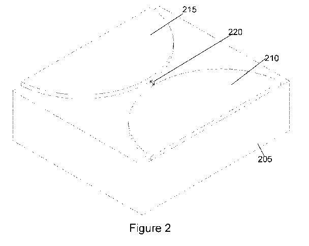
Figure 2 illustrates a three-dimensional view of a photodetector according to
one
embodiment or implementation. The photodetector includes a single absorption
region
(or absorption layer) 205. Two electrodes 210, 215 are disposed or formed on
the
absorption region spaced from one another. There is a (lateral) distance (or
separation)
220 between the two electrodes 210, 215. The absorption region 205 includes a
substantially un-doped material. In other words, the absorption region 205
includes an
intrinsic material. In this embodiment, both electrodes 210, 215 have
substantially the
same or equivalent curvatures. When a bias (or an electrical bias) of
sufficient
magnitude is applied across electrodes 210, 215, due to the curvature of the
electrodes
and the separation between them, an electric field is established between them
of the
requisite magnitude for avalanche multiplication to occur near them. It
will be
CA 03106027 2021-01-07
WO 2020/016564 PCT/GB2019/051977
11
appreciated that both the curvature and/or the distance 220 between the
electrodes
210, 215 determines the breakdown voltage. Given that no doping is used in the
absorption region, it is surprising that avalanche breakdown may be achieved
by
controlling the geometry (e.g. the curvature and/or electrode separation) of
the
electrodes.
Figure 3a illustrates a top view of an alternative photodetector according to
one
embodiment or implementation. Figure 3b illustrates a top view of the
photodetector
depicted in Figure 3a, in which electric field line distribution between two
electrodes is
shown. Two electrodes 305, 310 are disposed on the absorption region spaced
from
one another. The curvature and/or shape of both electrodes 305 and 310 are not
equivalent in this example, and are therefore referred to as being asymmetric.
For
example, the first electrode 305 has a predetermined curvature and the second
electrode 310 has a different arrangement or shape compared to the first
electrode
305. When a bias of sufficient magnitude is applied across the electrodes, an
enhanced electric field is established near electrode 305 as indicated by the
increased
density of field lines (see Figure 3b). This enhanced electric field may
result in
avalanche breakdown near the first electrode 305.
Figure 4a illustrates a top view of an alternative photodetector according to
one
embodiment or implementation. Figure 4b illustrates a top view of the
photodetector of
Figure 4a in which electric field line distribution between two electrodes is
shown. Two
electrodes 405, 410 are disposed on the absorption region spaced from one
another. In
this embodiment, the curvature and/or shape of both electrodes 405, 410 are
equivalent or substantially the same and are therefore referred to as being
symmetric.
When a bias of sufficient magnitude is applied across the electrodes, an
enhanced
electric field is established near electrode 415 near the curved electrodes
405, 410
(see Figure 4b), as indicated by the increased density of field lines. This
enhanced
electric field may result in avalanche breakdown near the electrodes 405, 410.
Figure 5a illustrates a top view of an alternative photodetector according to
one
embodiment or implementation. Figure 5b illustrates a top view of the
photodetector of
Figure 5a in which electric field line distribution between the electrodes is
shown. Four
electrodes 505, 510, 515, 520 are disposed on the absorption region spaced
from one
another. More electrodes are used in this example to increase the volume of
the
CA 03106027 2021-01-07
WO 2020/016564 PCT/GB2019/051977
12
detection region. In one example, the curvature and/or shape of electrodes
505, 510,
515, 520 could be symmetric. In an alternative example, the curvature and/or
shape of
the electrodes 505, 510, 515, 520 could be different and therefore the
electrodes 505,
510, 515, 520 may be asymmetric When a bias of sufficient magnitude is applied
across electrodes 505, 510, 515, 520 an enhanced electric field is established
near
them as indicated by the increased density of field lines (see Figure 5b).
This enhanced
electric field may result in avalanche breakdown near electrodes 505, 510,
515, 520.
Figure 6a illustrates a top view of an alternative photodetector according to
one
embodiment or implementation. Figure 6b illustrates a top view of the
photodetector of
Figure 6a in which electric field line distribution between the electrodes is
shown. In the
implementation of Figure 6a and Figure 6b, eight electrodes 605, 610, 615,
620, 625,
630, 635, 640 are disposed on the absorption region spaced from one another.
Like the
implementation of Figure 5, more electrodes are used in this example to
increase the
volume of the detection region. In one example, the curvature and/or shape of
the
electrodes 605, 610, 615, 620, 625, 630, 635, 640 are substantially the same
and
therefore the electrodes 605, 610, 615, 620, 625, 630, 635, 640 are symmetric.
In an
alternative example, the curvature and/or shape of the electrodes 605, 610,
615, 620,
625, 630, 635, 640 could be different and therefore the electrodes 605, 610,
615, 620,
625, 630, 635, 640 may be asymmetric. When a bias of sufficient magnitude is
applied
across electrodes 605, 610, 615, 620, 625, 630, 635, 640, an enhanced electric
field is
established near them as indicated by the increased density of field lines
(see Figure
6b). This enhanced electric field may result in avalanche breakdown near
electrodes
605, 610, 615, 620, 625, 630, 635, 640.
Figure 7a illustrates a top view of an alternative photodetector according to
one
embodiment or implementation. Figure 7b illustrates a top view of the
photodetector of
Figure 7a in which electric field line distribution between the electrodes is
shown. Ten
electrodes 705, 710, 715, 720, 725, 730, 735, 740, 745, 750 are disposed on
the
absorption region spaced from one another. The electrodes are organised, for
example, in an arrangement suitable for wavelength spectrometry. Like the
implementation of Figure 6, more electrodes are used in this example to
increase the
volume of the detection region. In one example, the curvature and/or shape of
the
electrodes 705, 710, 715, 720, 725, 730, 735, 740, 745, 750 are substantially
the same
and therefore the electrodes are symmetric. In an alternative example, the
curvature
CA 03106027 2021-01-07
WO 2020/016564 PCT/GB2019/051977
13
and/or shape of the electrodes 705, 710, 715, 720, 725, 730, 735, 740, 745,
750 could
be different and therefore the electrodes may be asymmetric. When a bias of
sufficient
magnitude is applied across electrodes 715, 720, 725, 730, 735, 740, 745, 750,
an
enhanced electric field is established near them as indicated by the increased
density
of field lines (see Figure 7b). This enhanced electric field may result in
avalanche
breakdown near electrodes 715, 720, 725, 730, 735, 740, 745, 750. This
configuration
may be used as part of a spectrometer when combined with a spectroscopic
technique
in which spatial separation of photons is obtained, such as refraction or
diffraction. The
spectral properties may be inferred from the position of photon incidence,
which itself
may be obtained from the electrode that collects the carriers.
Figure 10 (a) and Figure 10 (b) illustrate a three-dimensional view of a
photodetector
according to one embodiment or implementation. The photodetector device is
configured for integration with on-chip planar waveguides 1025. The
photodetector
includes a single absorption region (or layer) 1005. Two electrodes 1010, 1015
are
disposed on the absorption region spaced from one another. There is a distance
1020
between the two electrodes 1010, 1015. The absorption region 1005 includes a
substantially un-doped material. The contacts or electrodes 1010, 1015 may be
disposed on a step face (figure 10b) from a top surface, or on the top surface
(figure
10a).
Geometric Field Enhancement
We will now describe the theory behind the geometrical enhancement of the
electric
field that is here exploited for avalanche multiplication according to the
implementations
of the present disclosure. We will also discuss numerical simulation results.
According to Maxwell's equations, in the absence of a changing magnetic field
the
electric field E established between two electrodes is defined solely by the
gradient of
the electric potential Vrcp
E = ¨Vrcp,
(1)
where
äp äp _dcp
(2)
dx dy
CA 03106027 2021-01-07
WO 2020/016564 PCT/GB2019/051977
14
a vector whose magnitude quantifies the spatial rate of change of the electric
field at a
given point, and whose direction specifies its steepest increase from that
point.
From (1) and (2), it is not only evident that the bias applied across the
electrodes
affects the electric field established between them, but the very geometry
(e.g. the
curvature and/or shape and/or arrangement and/or electrode distance) of the
electrodes themselves does too. Specifically, the electric field magnitude
increases
both with the applied bias and electrode curvature, but decreases with
electrode
separation.
The salient facet of the present disclosure is inherent in the exploitation of
geometry,
and in particular electrode curvature, rather than doping, to enhance the
formation of
an electric field of the requisite magnitude for avalanche breakdown to occur
in a
prescribed material: thereby providing the necessary amplification of current
required
for single-photon detection.
For a linear, isotropic, and homogeneous medium Gauss's law defines the
electric field
established by a given distribution of charge p
V = E = ¨
(3)
ErE0'
where V = E is the divergence of the electric field
äEx äE dE,
V = E = ¨ + ¨ +
(4)
ax äy äz
a scalar quantifying the extent to which the electric field diverges from a
given point, Er
is relative permittivity of the medium, and Eo is the permittivity of vacuum.
In the case where the charge density is negligible, from (1) and (3)
ErE0V2(p = 0
(5)
where Vr2cp is the Laplacian of the electric potential
CA 03106027 2021-01-07
WO 2020/016564 PCT/GB2019/051977
a2(1) a2(1) _ä2p
(6)
V2
ax2 az2
a scalar quantifying the divergence of the gradient of the electric field at a
given point.
Both the bias Vg applied across the electrodes and the electrode geometry
provide the
5 necessary and sufficient boundary conditions to solve (5) for the
electric potential cp
over all space by the finite element method, before finally solving (1) for
the electric
field.
A selection of results of the 2D solutions to (5) and (1) are now presented.
These are
10 qualitatively similar to 3D simulations, which, for simplicity, are not
shown. We define
the field magnitude a as
a = (¨õ)10,
(7)
v g
where d is the electrode separation, Vg is the applied bias, and 1E1 is the
electric field
magnitude. It is important to note that the field magnitude is unitless.
15 Figure 8 is a plan profile of the field magnitude established between
the electrodes
(805 and 810) of nine different electrode geometries, each of equivalent
electrode
separation, but of varying electrode radii R. The ratio of the electrode
separation to
electrode radius is here termed the relative curvature clic, where K = 1IR is
the
curvature, and is varied in a binary geometric progression from 0.25 to 32.
The parallel
electrode case where dK=0 is included for comparison. For the parallel
electrode case
(top left), at all points between the electrodes 805, 810 the field magnitude
is unity (as
no variation shown between the electrodes 805, 810). For all other geometries
the
electrodes 805, 810 are curved, in proximity to which regions of field
enhancement
(white regions), where the field magnitude is greater than unity, can clearly
be
observed.
It is known that for two parallel electrodes 1E1 = , in which case from (7) a
= 1.
Accordingly, we define regions of field enhancement to be where a> 1, and
regions of
field diminishment to be where a < 1.
CA 03106027 2021-01-07
WO 2020/016564 PCT/GB2019/051977
16
Figure 9 illustrates field magnitudes along the line y = 0 for nine different
electrode
geometries of varying relative curvatures in Figure 8. The extent of field
enhancement
in the enhanced regions depicted in Figure 8 is investigated in Figure 9. In
the parallel
electrode case (top left of Figure 8), the field magnitude (see dic = 0) is
again confirmed
to be unity at all points between the electrodes. For all other geometries the
electrodes
are curved, and exhibit enhanced regions in proximity to the electrodes where
the field
magnitude is greater than unity. The degree of field enhancement within the
enhanced
regions can be observed to increase both with increasing electrode proximity,
and with
increasing curvature. It is noteworthy that for the curved electrodes the
electric field is
diminished with increasing proximity to the electrode separation centre-point.
The inset
clearly shows the degree of field enhancement near the left electrode (as both
electrodes have the exact same shape, the level of enhancement will be
identical for
the right electrode too), for relative curvatures dic > 256 the electric field
is enhanced
approaching the electrode interface by at least one order of magnitude. For
all curved
devices the enhanced region can be seen to extend at least 0.1d from each
electrode.
It is clear both from Figures 8 and 9 that increasing the electrode curvature
increases
the field enhancement in their proximity. The degree of enhancement
exponentially
increases with increasing curvature, and rapidly tends to infinity. The bias
VB applied
across the electrodes demands that an enhanced field is compensated for by a
diminishment field elsewhere, but it is important to stress that the magnitude
of the
diminished field will not generally be zero - meaning photon-induced carriers
created in
the diminished region will be still be driven to the enhanced regions as
intended.
Example of Single-photon Detection by Avalanche Breakdown
By operating a material at or above its breakdown field Eb ¨ a method of
operation
referred to as Geiger mode operation ¨ mobile charge carriers created by the
internal
photoelectric effect can gain enough kinetic energy from the electric field
for collisions
to be ionising: resulting in the creation of additional mobile charge carriers
for which the
process can repeat again. This mechanism, referred to as avalanche breakdown,
is
self-sustaining and produces a macroscopic mobilisation of charge from a
single
photon: resulting in a measurable detection signal. It will be appreciated
that the
present disclosure is not restricted to single-photon detection only.
CA 03106027 2021-01-07
WO 2020/016564
PCT/GB2019/051977
17
Breakdown Fields and Band Gaps
The following table details the breakdown fields of a number of different
materials,
sorted in order of increasing magnitude. The separation between two parallel
electrodes required to facilitate avalanche breakdown at an applied bias of
Vg= 10 V is
listed.
Material E b (MV M-1) d (pm) Band Gap (eV)
Band Gap (nm)
I nSb 0.1 100 0.17 7293
I no.53Ga0.4.7As 0.2 3.33 0.74 1675
I nAs 0.2 2.5 0.35 3502
GaSb 4 2 0.72 1707
Ge 10 1 0.66* 1875*
Si 30 0.33 1.12* 1107*
GaAs 40 0.25 1.42 871
C (Diamond) 50 0.2 5.46* 227*
I nP 50 0.2 1.34 922
A10.4.5Ga0.55As 50 0.2 1.99 626
GaP 100 0.1 2.26* 548*
AIN 200 0.05 6.03 205
BN 400 0.03 6.1* 203*
GaN 500 0.02 3.28 378
Table 1. Breakdown fields and band gaps. Sorted in order of increasing
magnitude, the breakdown
fields for a selection of materials are listed. For each material the
separation between two parallel
electrodes required to facilitate avalanche breakdown at and applied bias of
VB =10 V is listed along with
the material's band gap in units of eV and nm. * denotes the material has an
indirect band gap.
Geometric Field Enhancement Example
In one example only, for a GaAs device with an electrode separation of d = 1
pm, to
achieve breakdown at Vg= 10 V from (7) a field magnitude of a 4 is required,
which in
2D is achieved approaching the electrodes by a relative curvature of cbc = 64,
corresponding to a radius of R = 16 nm.
Experimental Results
Devices have been fabricated from semi-insulating gallium arsenide (GaAs) and
have
been evidenced to be capable of undergoing avalanche breakdown at low voltages
(for
CA 03106027 2021-01-07
WO 2020/016564 PCT/GB2019/051977
18
example, less than or equal to 10 V), and performing without amplification,
room-
temperature low-level light detection with response times below 100 ps.
General Principles of the Implementations
We will now discuss the general principles of the operation of the
photodetector device
of the present disclosure. These principles are applicable to all the devices
discussed
above in Figures 2 to 8. Generally speaking, charge carriers are generated in
the
absorber region both by the absorption of incident photons, and by thermal
excitation,
with the former being desirable, and the latter undesirable. Absorbed photons
will have
energy equal to or greater than the absorber's band gap, where the absorber
can be
chosen to suit a particular application but with the proviso that unwanted
thermally-
generated carriers will be more problematic for smaller band-gap materials.
Generated carriers may initiate an avalanche breakdown, which will depend on:
1. The location of their production. Though dependent on scattering
processes, carriers will tend to travel parallel to the electric field vector.
If
the carrier's path reaches an electrode without it encountering the
avalanche region, it will not cause an avalanche.
2. The applied bias, and the absorber's breakdown field value. The shape of
the electric field is independent of the applied voltage, but its magnitude is
not. Larger voltages will give larger avalanche regions, allowing more
generated carriers to contribute to the avalanche current. Similarly, a low
breakdown field will give a smaller avalanche volume.
3. Applied electric or magnetic fields, whether using external or integrated
devices, or fields such as would be generated by an absorber region which
is magnetic or exhibits a spin-hall effect. Electric fields will perturb the
absorber region electric field, and magnetic effects will deflect moving
carriers.
If a carrier reaches an avalanche region during the above-breakdown part of
the
periodic bias (gated-Geiger mode operation), it will, through impact
ionisation, generate
CA 03106027 2021-01-07
WO 2020/016564 PCT/GB2019/051977
19
a current additional to that which it contributes itself. If a carrier reaches
the electrode
without avalanching, this amplification effect is absent. Consequently, we can
define
from the electric field distribution a volume of the absorber in which carrier
generation
will lead to a measurable signal through avalanche multiplication. We
designate this
volume the detection region. The device should therefore be designed such that
photons of the desired wavelength will be absorbed in the detection region;
the
characteristic absorption depth should be optimised to reduce to an acceptable
degree
the fraction of photons passing through this volume. The detection region is a
subset of
the avalanche region.
Thermally-generated carriers are the source of unwanted dark current, and are
a
limiting factor to device operation. An important observation is that, though
all absorber
materials will have a finite rate of thermal generation of carriers, only
those created
within the detection region will be amplified on reaching the device
electrodes. In
principle at least, it is therefore not necessary to provide electrical
isolation for the
device.
Manufacturing or Realisation of the Disclosed Device
We will now discuss the manufacturing of the disclosed photodetector. The
following
comments are applicable to all the devices (in Figures 2 to 8) discussed in
the present
disclosure. The device may be made in many ways; its simplest configuration is
the
forming of two or more electrodes directly on the surface of the absorber
material, with
those electrodes connected to external control circuitry. The electrodes may
be metal,
or metal multilayers, but may also be semiconductors such as polysilicon or a
layer or
layers formed during the growth of the absorber; the necessary conditions are
that the
device is not significantly degraded by electrical resistance or intermediate
insulating
layers, and that the Fermi level in the conductor should align with the band
structure of
the absorber material at a point within the band-gap such that carrier
injection from the
contacts is not significant. The absorber (or the absorption region) itself is
intended to
be as free as possible of electrical carriers for reasons stated below, but
the principle of
geometric enhancement is also, but with lesser utility, applicable to Schottky-
type
contacts separated by a carrier-rich region. Cooling of the sample using a
Peltier
device may be practical, and cryogenic techniques may be necessary for
detecting
lower-energy photons or for very low photon fluxes.
CA 03106027 2021-01-07
WO 2020/016564 PCT/GB2019/051977
Devices of the simplest type may be made by standard lithographic techniques
using
resist and the appropriate exposure and development. Generally speaking,
techniques
for doing this include:
5
1. Lift-off, in which the contact material, usually a metal or multilayer of
metals,
is deposited onto a lithographically-patterned surface. The resist is removed
chemically, leaving the contact material only in the desired areas.
Deposition here is best suited to a highly-directional technique such as
10 resistive thermal or electron-beam evaporation, putting technical
limitations
on the choice of materials, but is often ideal for metals.
2. Etch-back, which involves the formation of a layer of contact material
across
the entire surface, followed by lithography and chemical- or plasma-etching
15 of the unwanted material.
Many techniques are suitable for layer
deposition, including evaporative deposition, in-situ epitaxial growth such as
molecular-beam or chemical epitaxies, or sputter-deposition.
Generally, the reflection of photons from the device surface will reduce
detection
20 efficiency. This may be addressed by techniques including anti-
reflection coatings or
layers. Similarly, a buried reflector stack may be used to reflect photons
which would
otherwise travel beyond the detection region.
It may be useful to tailor the electric-field profile in the device by
patterning the
absorber using the above (or other) processes. Etching of the absorber (or
absorption
region) prior to deposition could permit the recessing of contacts to optimise
the
detectable volume; the thickness of the detection region will be enhanced in
this kind of
structure. This may also be useful if surface recombination is a problem, as
carriers
would be drawn away from the surface by the field profile.
Recombination of carriers before avalanching results in a reduced responsivity
and
detection efficiency, and the time taken for carriers to traverse the device
may limit its
bandwidth. However, in the present device, the use of insulating or intrinsic
semiconducting material improves both; the scarcity of free carriers strongly
inhibits
recombination and reduces the screening effects which limit electric field in
conductors
CA 03106027 2021-01-07
WO 2020/016564 PCT/GB2019/051977
21
and doped semiconductors, leading to higher drift velocity and thus faster
transit and
higher bandwidth.
The dark current might be large enough that isolation of some kind is
desirable. A way
to achieve this would be to incorporate a wider-gap barrier layer below the
detection
region, minimising the bulk generation of carriers and/or blocking the
progress of those
carriers towards the surface. This may be improved further by mesa-etching the
absorber such that as large an area as possible of the contacts lies on the
barrier
material. The removal by etching of a sacrificial buried layer, a thinning of
the entire
substrate, or using a free-standing thin film as the absorber may have a
similar effect.
It will be appreciated that all doping polarities and/or voltage polarities
mentioned
above or shown in the figures could be reversed, the resulting devices still
being in
accordance with the present disclosure.
The skilled person will understand that in the preceding description and
appended
claims, positional terms such as 'above', 'overlap', 'under', 'lateral',
'vertical', etc. are
made with reference to conceptual illustrations of a photodetector device,
such as
those showing standard cross-sectional perspectives and those shown in the
appended drawings. These terms are used for ease of reference but are not
intended
to be of limiting nature. These terms are therefore to be understood as
referring to a
photodetector when in an orientation as shown in the accompanying drawings.
Although the invention has been described in terms of preferred embodiments as
set
forth above, it should be understood that these embodiments are illustrative
only and
that the claims are not limited to those embodiments. Those skilled in the art
will be
able to make modifications and alternatives in view of the disclosure which
are
contemplated as falling within the scope of the appended claims. Each feature
disclosed or illustrated in the present specification may be incorporated in
the
invention, whether alone or in any appropriate combination with any other
feature
disclosed or illustrated herein.