Note: Descriptions are shown in the official language in which they were submitted.
CA 03106857 2021-01-18
WO 2020/018002
PCT/RU2019/050105
ELECTROCHROMIC MATERIAL AND METHOD OF MANUFACTURING THEREOF
Field of the invention
[0001] The present invention relates to electrochromic field, in particular,
to electrochromic (EC)
materials of neutral to eye colors, and to methods of manufacturing such
materials. More
particularly, the present invention relates to the field of inorganic EC
materials with advanced
characteristics and to their manufacturing technologies aimed at obtaining
optimal material
structure. The materials possess extended color range (tints of blue, gray,
black, brown) as well
as higher conductivity, which allows deposition of thicker EC layers (up to 10
[tm) without a
dramatic drop in their performance. In addition, the materials are promising
for the use as
cathode materials in primary or secondary energy sources.
Background of the invention
[0002] Over the past several decades, tungsten oxide (W03) had been
extensively studied due to its
interesting physical and chemical properties. W03 shows a strong reversible
field-aided ion
intercalation behavior. Ions such as Lit, Nat, Kt, etc. may be easily
introduced into the host W03
matrix. This ion insertion is combined with a strong change in the electronic
and optical
properties of the oxide, and this effect is exploited intensively in EC
devices, such as large area
information displays, rear-view mirrors, smart windows for automobiles and
energy saving
architecture due to their low power consumption and high energy efficiency [1-
4]. Amorphous
W03 film synthesized by magnetron sputtering has shown to be an excellent
candidate for EC
applications 115, 6]. When ions are intercalated, the charge-compensating
electrons enter the
localized states. The electronic structure of W03 is modified, and this
strongly alters the optical
properties of the material from transparent to a deep blue color. A number of
dopant and
approaches for the doping the host amorphous W03 material by transition metals
and
nonmetallic elements have been investigated for the enhancement of their EC
and
electrochemical properties [7-16].
[0003] U.S. Patent Publication No. 2007097480A1 discloses an electrochromic
single-phase compound
of formula Wi_xTax03-x/2, wherein x has a value in a range of approximately
0.15 to
approximately 0.5, produced by pulse laser deposition as a thin film. In
particular, U.S. Patent
Publication No. 2007097480A1 discloses Ta0.1W0.902.95 changing color from
light pink to cadet
blue, and Ta0.3W0.702.85 from light green to light brown-green under tit ion
intercalation at ¨
CA 03106857 2021-01-18
WO 2020/018002
PCT/RU2019/050105
2
0.7 V. The electrochromic material may be used in "smart" windows, mirrors,
information
displays and variable emittance surfaces. However, U.S. Patent Publication No.
2007097480A1
fails providing a neutral color at colored and bleached states.
[0004] U.S. Patent Publication No. 2009323157A1 discloses an electrochromic
material including at
least one of the following compounds: oxides of tungsten (W), niobium (Nb),
tin (Sn), bismuth
(Bi), vanadium (V), nickel (Ni), iridium (Ir), antimony (Sb) and tantalum
(Ta), alone or as a
mixture, and optionally including an additional metal such as titanium (Ti),
rhenium (Re) or
cobalt (Co), possible to switch glazing between a bleached state and a colored
state characterized
by a light transmission of 55/2.5%, 50/1%, 40/0.01%. However, U.S. Patent
Publication No.
2009323157A1 is silent on providing a neutral color at colored and bleached
states.
[0005] U.S. Patent Publication No. 2010245973A1 discloses an electrochromic
material based on W03_
y (0<y 0.3), where intercalation of lithium ions into tungsten oxide causes
the tungsten oxide to
change from transparent (bleached state) to blue (colored state), and
generally mentions a nickel
tungsten oxide turning from a transparent state to a brown colored state.
However, U.S. Patent
Publication No. 2009323157A1 is silent on chemical composition of the "nickel
tungsten oxide".
[0006] U.S. Patent Publication No. 2014002884A1 discloses an electrochromic
material chosen among
hydrated metal oxides, preferably amorphous, such as hydrated tungsten oxide
HxWO3mH20,
where x is between 0 and 1 and n is an integer of 1 to 2, and mixtures of two
or more of these
oxides. However, U.S. Patent Publication No. 2014002884A1 is silent on
providing a neutral
color at colored and bleached states.
[0007] U.S. Patent Publication No. 2014043666A1 discloses an electrochromic
material selected from
the group consisting of Lii82NiWo 450x; Li
97NiZr0230x; Lio 5iNiZro 16Lao 190x;
Li222NiZro 14Moo 250x; Li3i2NiZr0 isTa0150x; and Li265NiZr0 i8V0600x, where x
ranges from
approximately 0.1 to approximately 50, from approximately 1 to approximately 6
or from
approximately 1.6 to approximately 5.4, which it is proposed to be combined
with dark blue
electrochromic tungsten oxide, to yield a more neutral grey dark state for the
overall
electrochromic coating. However, U.S. Patent Publication No. 2009323157A1 is
silent on
chemical composition of the "tungsten oxide". Moreover, the document states
that one sample
exhibited a repeatable bleaching time of approximately 11 seconds, and a
coloration time of
approximately 11 seconds with corresponding bleached and dark state for light
transmission at
670 nm of 98/50%, another sample exhibited corresponding values of
approximately 25 seconds,
CA 03106857 2021-01-18
WO 2020/018002
PCT/RU2019/050105
3
approximately 12 seconds, and approximately 94/26%, so the electrochromic
material of U.S.
Patent Publication No. 2009323157A1 is rather slow.
[0008] U.S. Patent Publication No. 2017003564A1 discloses electrochromic
materials, which may be
binary metal oxides (e.g., oxides that include two metals in addition to
lithium or other
transported ion, NiWO being one example), ternary metal oxides (e.g., oxides
that include three
metals, NiWTa0 being one example), or even more complex materials. It is
generally stated that
they are doped or otherwise combined with one or more additional elements. The
additional
element(s) may include at least one a non-alkali metal in various cases. The
electrochromic
materials may comprise one or more additional element selected from the group
consisting of:
silver (Ag), aluminum (Al), arsenic (As), gold (Ag), barium (B a), beryllium
(Be), bismuth (Bi),
calcium (Ca), cadmium (Cd), cerium (Ce), cobalt (Co), chromium (Cr), copper
(Cu), europium
(Eu), iron (Fe), gallium (Ga), gadolinium (Gd), germanium (Ge), hafnium (Hf),
mercury (Hg),
indium (In), iridium (Ir), lanthanum (La), magnesium (Mg), manganese (Mn),
molybdenum
(Mo), niobium (Nb), neodymium (Nd), osmium (Os), protactinium (Pa), lead (Pb),
palladium
(Pd), praseodymium (Pr), promethium (Pm), polonium (Po), platinum (Pt), radium
(Ra), rhenium
(Re), rhodium (Rh), ruthenium (Ru), antimony (Sb), scandium (Sc), selenium
(Se), silicon (Si),
samarium (Sm), tin (Sn), strontium (Sr), tantalum (Ta), terbium (Tb),
technetium (Tc), tellurium
(Te), thorium (Th), titanium (Ti), thallium (T1), uranium (U), vanadium (V),
tungsten (W),
yttrium (Y), zinc (Zn), zirconium (Zr), and combinations thereof. In certain
embodiments, the
additional element(s) may include at least one element selected from the group
consisting of
tantalum, tin, niobium, zirconium, silicon, aluminum, and combinations
thereof. In particular, it
discloses a material of LiaNiW,Ay0z, where: a is 1 to 10; x is 0 to 1; y is 0
to 1; and z is at least
1; and wherein a, x, y, z, and A are selected independently for each of the
first and second
sublayers of the counter electrode layer, and NiWTa0 including approximately
7% or 14%
tantalum. However, U.S. Patent Publication No. 2017003564A1 is silent on
providing a neutral
color at colored and bleached states.
[0009] U.S. Patent Publication No. 2017329200A1 discloses an electrochromic
material containing any
one or more of a number of metal oxides including tungsten oxide (W03),
molybdenum oxide
(Mo03), niobium oxide (Nb2O5), titanium oxide (TiO2), copper oxide (Cu0),
iridium oxide
(Ir203), chromium oxide (Cr2O3), manganese oxide (Mn203), vanadium oxide
(V205), nickel
oxide (Ni203), cobalt oxide (Co203) and the like. The metal oxide may be doped
with one or
CA 03106857 2021-01-18
WO 2020/018002
PCT/RU2019/050105
4
more dopants such as lithium, sodium, potassium, molybdenum, niobium,
vanadium, titanium,
and/or other suitable metals or compounds containing metals. Mixed oxides (for
example, W¨
Mo oxide, W¨V oxide) also may be used so the electrochromic layer may include
two or more of
the aforementioned metal oxides. However, U.S. Patent Publication No.
2017329200A1 is silent
on providing a neutral color at colored and bleached states.
[0010] US Patent No. 6266177B1 discloses technology of producing
electrochromic materials like
CU0.064W0.930y, 1(0.1W0.90y, Na0.1W0.90y, Li0.1W0.9 y, Ba0.1W00.90y,
(Li0.1Cr0.1W0.8)0y,
(Li0.1C00.1W0.8)0y. However, US Patent No. 6266177B1 is silent on providing a
neutral color at
colored and bleached states.
[0011] Patent documents W02011028253A2, W02011028254A2 disclose an approach to
providing
electrochromic material having improved color properties. In terms of
color/hue, certain
embodiments may reduce the yellowish hue in the clear state and the multiple
colors that
sometimes are present in the tinted state by ensuring delta E, which may be
less than
approximately 1.5 eV, more preferably less than approximately 1.25 eV, and
still more
preferably less than approximately 1 eV, while value of x preferably is
2.4<x<3; more preferably
2.6<x<3 in sub-stoichiometric WO,, instead providing a more neutral color in
the clear state with
a choice from one of multiple colors in the tinted state.
[0012] Patent documents W02011137080A1, W02011137104A1 and W02012177790A2
disclose an
electrochromic material W03_,, (0<y<0.3) and nickel-tungsten oxide (NiWO)
counter-electrode
with tantalum dopant to provide a neutral color at bleached state. However,
W02011137080A1
is silent on providing a neutral color at colored state.
[0013] Patent document W02013013135A1 discloses, inter alia, an electrochromic
material Li,Ni(II)(i_
3,)Ni(III)(y)Wz0(i+o.sx+o.sy+3z). However, W02013013135A1 is silent on
providing a neutral color at
colored and bleached states.
[0014] Patent documents W02014113796A1 and W02014113801A1 disclose a lithium
tungsten nickel
oxide film as an electrochromic material. However, W02014113796A1 is silent on
providing a
neutral color at colored and bleached states.
[0015] Patent document W02014143410A1 discloses an electrochromic material
having an atomic ratio
of amount of lithium to combined amount of nickel and tungsten (i.e., Li:
[Ni+W]) or combined
amount of nickel, molybdenum and tungsten (i.e., Li:[Ni+Mo+W]) in the
electrochromic layer is
generally at least approximately 0.4:1, 0.75:1, 0.9:1 and generally less than
1.75:1. The
CA 03106857 2021-01-18
WO 2020/018002 PCT/RU2019/050105
document also discloses an electrochromic material having an atomic ratio of
the combined
amount of molybdenum and tungsten to the combined amount of nickel, molybdenum
and
tungsten (i.e., [Mo+W]:[Ni+Mo+W]) is greater than approximately 0.8:1, 0.7:1,
0.6:1 or 0.5:1.
The document also discloses an electrochromic material having an atomic ratio
of the combined
amount of molybdenum, tungsten and bleached state stabilizing element(s) M to
the combined
amount of nickel, molybdenum, tungsten and bleached state stabilizing elements
M in the
electrochromic lithium nickel oxide material (i.e., [Mo+W+M]:[Ni+Mo+W+M]),
where M is Y,
Ti, Zr, Hf, V, Nb, Ta, B, Al, Ga, In, Si, Ge, Sn, P, Sb or a combination
thereof) is less than
approximately 0.8:1, 0.7:1, 0.6:1 or 0.5:1 but greater than approximately
0.075:1. However,
W02014143410A1 is silent on providing a neutral color at colored and bleached
states.
[0016] Patent document W02017034847A1 discloses an electrochromic material in
a form of cubic or
hexagonal cesium doped tungsten oxide nanoparticles having improved color
properties, in
particular, CsxWO3(where 0.2<x<0.4), CsiW06_, (where 0<a<0.3), NbOx, TiO2,
M003, Ni02,
V205 or combinations thereof. For example, to produce a blue color, the
electrochromic material
may include approximately 100 wt.% of W03 as the first nanostructures and may
omit the
second nanostructures; to produce a green color, the electrochromic material
may include
approximately 60 wt.% of Cs().29W03, hexagonal crystal lattice structure
nanocrystals, and
approximately 40 wt.% of indium tin oxide (e.g., Sn:In203) nanocrystals; to
produce a brown
color, the electrochromic material may include approximately 100 wt.% NbO,
nanoparticles
(e.g., Nb2O5_, where 0<a<0.1) as the first nanostructures and may omit the
second
nanostructures; to produce a purple color, the electrochromic material may
include
approximately 100 wt.% Nb:TiO2 nanocrystals as the first nanostructures and
may omit the
second nanostructures; to produce a neutral gray color, the first
nanostructures may include
amorphous niobium oxide nanoparticles (e.g., Nb205_5, where 0<a<0.1), and the
second
nanostructures may include cesium doped tungsten oxide nanoparticles having a
cubic crystal
lattice structure (e.g., CsW206_5 nanocrystals, where 0<a<0.3).
[0017] Patent document W02017136243A1 proposes using 5-10 wt% of amorphous
nanostructured
materials like NbO, for color balancing to the visible light absorption in
electrochromic materials
due to the polaron-type shift in the spectral absorption of the doped-
transition metal oxide bronze
like CsiW206,, where 0<x<0.1.
CA 03106857 2021-01-18
WO 2020/018002
PCT/RU2019/050105
6
[0018] Patent document W02017165834A1 discloses an electrochromic material
that is made
substantially of WOK, where x is between approximately 2.7 and 3.5. However,
W02017165834A1 is silent on providing a neutral color at colored and bleached
states.
[0019] Non-patent document [18] discloses intercalation and conversion
processes related to atoms of
Li, Na and Ca in a crystal lattice of W03, used in electrochemical elements
and electrochromic
devices.
[0020] Non-patent document [19] discloses an effect of lithium concentration
in amorphous W03 on
optical properties of tungsten oxide-based films.
[0021] Non-patent document [20] discloses an effect of lithium concentration
in amorphous W03 on
spectral dependence of transmission factor and reflection factor of tungsten
oxide-based films.
[0022] Non-patent document [21] discloses a lithium intercalation process
related to different
electrolytes in electrochromic materials based on tungsten and nickel oxides.
[0023] Non-patent document [22] discloses an effect of lithium concentration
in W03 on spectral
dependence of optical properties.
[0024] Non-patent document [23] discloses an effect of nitrogen doping on
electrochromic properties of
W03.
[0025] Non-patent document [24] discloses an effect of W03 reduction degree on
electrochromic
properties of W03.
[0026] Non-patent document [25] discloses an effect of lattice structure type
of W03 on electrochromic
properties of W03. A possibility of doping W03 with titanium is indicated.
[0027] Non-patent document [26] discloses different aspects of providing
combined
electrochromic/storage devices based on W03.
[0028] Non-patent document [27] discloses an effect of doping W03 with
molybdenum on spectral
dependence of optical properties of W03.
[0029] Non-patent document [28] discloses an effect of W03 reduction degree on
electrochromic
properties of W03.
[0030] Non-patent document [29] discloses an effect of annealing on optical
properties of tungsten
oxide with stoichiometric content of W18049 compared to ordinary tungsten
oxide W03.
[0031] Conventional electrochromic materials obtained according to known
technology have a fixed tint
color, mostly blue, which may be uncomfortable for some users and even
inapplicable in some
cases, e.g., due to safety reasons. Fixed color means here that the prior art
technology is mostly
CA 03106857 2021-01-18
WO 2020/018002
PCT/RU2019/050105
7
unable to provide any selection of available colors during production.
Further, conventional
electrochromic materials have a limited lifetime. Moreover, conventional
electrochromic
materials have a long transitional time when changing from colored to
transparent state and back.
[0032] Accordingly, there is a need in the art for relatively cheap
electrochromic materials and
technology for industrial and/or domestic application, which would provide
extended tint color
range, including optically neutral colors like gray or brown, improved
lifetime, and shortened
transitional time. Preferably, such materials would be also structurally and
technologically
compatible with photovoltaic devices like solar batteries and with energy
storing devices like
lithium batteries or supercapacitors. This compatibility would allow using a
unified technology
and providing combined devices like smart glasses having controllable
transparency and capable
of producing and storing electrical energy.
Summary of the invention
[0033] Magnetron sputtering and co-sputtering for producing EC materials may
be performed by PDC
method in several ways: (1) directly from carbide-based material targets such
as WC, MoC, CrC,
SiC, VC, Ni3C, Co2C, NbC-Nb2C, TaC, SiC, Mn5C2, etc.; (2) from relevant
transition metals W,
Mo, Cr, Al, Ti, Zr, Nb, Ni, V, Ta, Mn and graphite-based material target as
well as non-metal
elements such as Si, Ge, P, B, etc.; (3) directly from composite targets (fine
powder mixture of
transition metals, non-metal elements and graphite powder). Sputtering may be
performed
instantly from 1 to 4 targets in each case.
[0034] The proposed sputtering method allows for obtaining EC materials with
increased electronic and
ionic conductivity, higher coloration and good cycling (lifetime). Moreover,
the inventors have
obtained other tints of blue as well as gray, black and brown colors neutral
to the eye.
[0035] The proposed technology provides an electrochromic material having a
formula W02.4
2 9:M 1 :M2:E1 :E2:E3, where M1 is a dopant selected from Mo, Ti, Ni, Zr, V,
Cr, Al, Nb, Ta, Co,
Mn; M2 is an optional dopant selected from Mo, Ti, Ni, Zr, V, Cr, Al, Nb, Ta,
Co, Mn; here, El
is a dopant selected from H, N, C, Si, Ge, P, B; E2 is a dopant selected from
H, N, C, Si, Ge, P,
B; E3 is an optional dopant selected from H, N, C, Si, Ge, P, B; M1 M2, El E2
E3.
[0036] In particular, the electrochromic material may be M(I)0 1_3 0W02 4_2
9:M1 :M2:El:E2:E3, where
M(I) is selected from group 1 elements: Lit, Nat, Kt; it may be M(Tho sW02 4-
2 9:M 1 :M2:E1 :E2:E3, wherein M(II) is selected from group 2 elements: Mg2+,
Ca2+, Ba2+, Zn2+; it
may also be M(ITho oW02 4_2 9:MLMIELE2:E3, wherein M(III) is selected from
group 3
CA 03106857 2021-01-18
WO 2020/018002
PCT/RU2019/050105
8
elements: Sc3+, Y3+, La3+ and other lanthanides i.e., Ce3+, Pr3+, Nd3+, Pm3+,
Sm3+, Eu3+, Gd3+,
Tb3+, Dy3+, Ho3+, Er3+, Tm3+, Yb3+, Lu3+.
[0037] For co-sputtering, a combination of gas mixtures may be used: Ar/02/N2,
Ar/H2/N2/02,
Ar/NH3/02, Ar/CO/N2/02, Ar/CO/H2/N2/02, Ar/CH4/N2/02 and Ar/NH3/CO/N2/02. The
pressure
of the gas mixture may be between approximately 5 millitorr and approximately
15 millitorr, and
the gas mixture flow may be between approximately 80 sccm (standard cubic
centimeters per
minute) and approximately 100 sccm.
[0038] Further, the EC material may be pre-intercalated with Lit, Na + or K.
Alternatively, the EC
material may be pre-intercalated with Mg2+, Ca2+, Ba2+ or Zn2+. Still
alternatively, the EC
material may be pre-intercalated with Sc3+, Y3+, La3+, Ce3+, Pr3+, Nd3+, Pm3+,
SM3+, Eu3+, Gd3+,
Tb3+, Dy3+, Ho 3+, Er 3+, Tm3+, Yb3+, Lu3+. Pre-intercalation may be performed
in a liquid cell
using absolutized organic or inorganic electrolytes in argon atmosphere.
[0039] Further processing depends on the above pre-intercalation options. If
the EC material was not
pre-intercalated, it undergoes post-annealing at a temperature between
approximately 450 C and
approximately 550 C. No deintercalation needs to be performed in this case.
[0040] If the EC material was pre-intercalated with Lit, Na + or K+, it is
thermo-splitted by post-
annealing at a temperature between approximately 250 C and approximately 450
C and further
deintercalated under negative polarity in a liquid cell ions at approximately
room temperature (in
the case of using Na + or K+ ions for pre-intercalation). The deintercalation
procedure is not
necessary to perform when using Li + ions.
[0041] If the EC material was pre-intercalated with Mg2+, Ca2+, Ba2+ or Zn2+,
it is thermo-splitted by
post-annealing at a temperature between approximately 250 C and approximately
450 C and
further deintercalated under negative polarity in a liquid cell at
approximately room temperature.
[0042] If the EC material was pre-intercalated with Sc3+, Y3+, Ln3+
(lanthanides), it is thermo-splitted by
post-annealing at a temperature between approximately 100 C and approximately
250 C and
further deintercalated under negative polarity in a liquid cell at
approximately room temperature.
[0043] When the EC material was pre-intercalated with large atoms (e.g., Zn2+,
Ca2+, Y3+, etc.), splitting
(i.e., forming vertical nano-channels facilitating movements of Li + ions
during operation of the
EC material) may take place at a lower temperature, sometimes even at room
temperature. The
more pre-intercalated atom radius, the lower the splitting temperature may be.
CA 03106857 2021-01-18
WO 2020/018002
PCT/RU2019/050105
9
[0044] Post-annealing allows for fast switching and deep coloring/decoloring
EC material having stable
electrochemical characteristics and a long lifetime.
[0045] The EC material obtained by the above method is at least partially a
crystalline material. It may
be used as a cathode material or as an anode material, depending on
configuration of the EC
device layer stack.
[0046] As a result, the inventors have obtained a tungsten oxide EC material
(W024-
29:M 1 :M2:E1 :E2:E3) heavily doped with metals Ml, M2 = Mo, Ti, Ni, Zr, V,
Cr, Al, Nb, Ta,
Co, Mn, and nonmetals El, E2, E3 = H, N, C, Si, Ge, P, B. The main element in
each case is W
with a concentration of tungsten oxide in the final deposited film of more
than approximately
50% towards dopant concentration.
[0047] Additional features and advantages of the invention will be set forth
in the description that
follows, and in part will be apparent from the description, or may be learned
by practice of the
invention. The advantages of the invention will be realized and attained by
the structure
particularly pointed out in the written description and claims hereof as well
as the appended
drawings.
[0048] It is to be understood that both the foregoing general description and
the following detailed
description are exemplary and explanatory and are intended to provide further
explanation of the
invention as claimed.
Brief description of the attached drawings
[0049] The accompanying drawings, which are included to provide a further
understanding the
invention and are incorporated in and constitute a part of this specification
and together with the
description serve to explain the principles of the invention.
[0050] In the drawings:
[0051] FIG. 1 illustrates an electrochromic stack;
[0052] FIG. 2A and FIG. 2B illustrate "wet" cells to perform lithium
intercalation (FIG. 2A) and
deintercalation (FIG. 2B) for optical measurements;
[0053] FIG. 3 illustrates dependence of optical transmittance (T) of EC layer
on degree of Li+
intercalation, where 1C is an average fast reversible capacity (approximately
13 mAh/g) of
galvanic cells with variety of heavily doped EC materials used as cathode. The
transmittance
drops down under increase of intercalated Li + ions in WOK-based materials.
CA 03106857 2021-01-18
WO 2020/018002
PCT/RU2019/050105
[0054] FIG. 4 illustrates dependence of transmittance of an EC doped tungsten
oxide Li,WA1CN02.9
(WA1CON) material in a visible range on degree of Lit concentration in the
intercalated material.
Detailed description of embodiments of the invention
[0055] Reference will now be made in detail to the preferred embodiments of
the present invention,
examples of which are illustrated in the accompanying drawings.
[0056] Electrochromic (EC) materials were developed, based on the heavily
doped tungsten oxide
W02.4_2.9:M 1 :M2:ELE2:E3 (where Ml, M2 = Mo, Ti, Ni, V, Cr, Al, Nb, Ta, Co,
Mn; El, E2, E3
= H, N, C, Si, Ge, P, B). When these materials are cathode materials
intercalated with metal ions,
they are not only intensively colored in various tints of blue (cold blue,
violet, gray blue, etc.),
but in some cases the new materials are colored in such "neutral" colors as
gray, black and
brown. Transparency of the obtained materials ranges from T? 76% in the
bleached state to T <
0.3% in the colored state and surpasses many existing commercial products. In
some cases at full
coloring in the samples, the films may be completely non-transparent in the
visible light range.
[0057] Doping the WO, host material was performed either by magnetron reactive
co-sputtering metals
and carbide materials or by reactive co-sputtering metals and graphite. Use of
carbide materials
as targets or co-sputtering metal and graphite is an important condition for
obtaining EC
materials W02.4_2.9:M1:M2:E1 :E2: E3 with advanced characteristics.
[0058] The obtained materials were post-annealed at a comparatively high
temperature (450-550 C).
Accordingly, the materials were crystalline. Different publications often show
diametrically
opposed opinions on effectiveness of amorphous and crystalline EC materials
based on tungsten
oxide. The inventors studied many samples of doped materials W02.4_2.9:M 1
:M2:E1 :E2:E3 and
conclude that crystalline structures are far more effective and stable when
used as EC layers. The
highest temperature of post-annealing EC sputtered materials known from open
sources usually
does not exceed 350-360 C [17], while a much higher temperature (up to 800
C) is usually
used in sol-gel technology during sintering small particles for EC layer
formation.
[0059] EC films obtained by this method possess increased electron
conductivity and a more porous
structure. It facilitates intercalation and de-intercalation of positive ions
(1-1 , Lit, Nat, Kt, Ca2t,
Mg2t, Zn2t, y3t, Sc3t, La3t, etc.) avoiding destruction of the EC coating. In
addition, the
proposed approach allows for application of quite thick EC layers (up to 10
[tm) while
maintaining an acceptable speed of coloring and bleaching. Consequently, it
allows achieving
more intense coloring in depth of EC coatings. This is especially important in
cases when the
CA 03106857 2021-01-18
WO 2020/018002
PCT/RU2019/050105
11
necessary depth of color or tint may not be achieved by another method. In
other words, when
intensity of the color of the material itself is low, a desired grade of
transmittance (T) in the
colored state in the visible range may be achieved owing to larger thickness
of the coating [30].
[0060] Depending on a value of electrochemical potential of the counter
electrode used in the cell, the
W02 4-2 9: M 1 M2:E1:E2:E3 materials obtained by the inventors may be used as
either cathode or
anode EC material. When the counter electrode is made of a metal foil or a
graphite-based
material or some oxide-based material or phosphate-based material like
Li4Ti5012, Ce02,
LiMn02, Nb2O5, TiO2, LiFePO4, etc., all having a rather low electrochemical
potential (usually
less than 3.3-3.5V compared to Li/Li), the W024_29:M1:M2:E1 :E2:E3 materials
may be used as
cathode EC materials. In other words, when the cell containing the cathode EC
material is
discharged (does not have any stored charge), the EC layer is completely
intercalated (e.g., by
Li + ions) and is in the colored state. Thus, power is not consumed for
maintaining the EC
material in the colored state in this kind of configuration. This option
allows saving energy, if the
EC material mostly has to be in the colored state. For example, it may be
advantageous when the
EC material is used for providing facade glazing operable under high
insolation conditions. In
this case, the EC material may be powered down for most of time and still
assure defending inner
space against solar irradiation, and it may be powered up for a short time
when the glazing needs
to be in the colorless state.
[0061] When the counter electrode is made of a material having a high
electrochemical potential
(usually more than 3.3-3.5V compared to Li/Lit) like V205, LiCo02, LiNi02,
LiNiCo02, etc.,
the W02 4-2 9:M1 :M2:E1:E2:E3 materials may be used as anode EC materials. In
other words,
when the cell containing the anode EC material is discharged (does not have
any stored charge),
the EC layer is completely deintercalated and is in the colorless state. Thus,
power is not
consumed for maintaining the EC material in the colorless state in this kind
of configuration.
This option allows saving energy, if the EC material mostly has to be in the
colorless state. It
may be advantageous when the EC material is used for applications requiring to
pass as much
sun or other light as possible for most of time, for example, in home interior
solutions or in car
dimmable glass.
[0062] In addition, films of EC materials W02 4_2 9:M 1 :M2:El:E2:E3 obtained
by co-sputtering carbides
and co-sputtering with graphite may be used for electrodes with advanced
properties for
electrochemical power sources like batteries and supercapacitors
(pseudocapacitors or hybrid
CA 03106857 2021-01-18
WO 2020/018002
PCT/RU2019/050105
12
capacitors) [31]. These materials are more promising if compared to existing
conventional
cathode materials based on cobalt, nickel and manganese oxides, as their real
capacity for Li/Li'
may be much higher, lifetime many times longer, and operating temperature
range quite wide (-
50... +150 C). This greatly expands the range of applications of such power
sources.
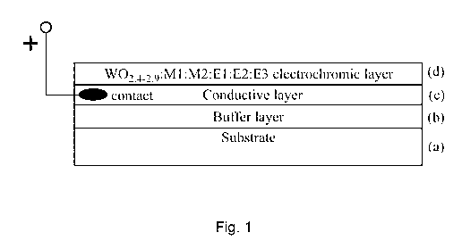
Materials
[0063] Magnetron sputtering of all materials was performed on rigid and
flexible substrates (a) (FIG. 1).
The buffer layer (b) may be sputtered before conductive layer (c). The
following combinations of
(a), (b) and (c) may be used: (glass or ceramic)/Si02/ITO, glass/SiC,0y/FTO,
(PET or
PEN)/Si02/ITO films (in some cases at relatively low temperatures) or any
other transparent
substrates for the transparent electrode assembly as well as non-transparent
or minor electrodes
such as (glass or ceramic)/M, Kapton /Si02/ITO, Kapton /M, (PEN or PET)/M (M =
Al, Ti,
Mo, Cr, NiCr or any suitable reflective metal) to perform optical and
electrochemical
measurements in a liquid cell (FIG. 2A, FIG. 2B). Thickness of the substrate
may also vary.
The thickness is usually 20 to 250 um for flexible polymer films or some thin
flexible ceramics
and 0.45 to 4 mm for glass, ceramics and other rigid substrates. Buffer layer
(b) in some
substrates is necessary to apply and its thickness ranges from 50 to 200 nm.
Electron-type
conductive layer (c) has a thickness of approximately 150-250 nm for ITO, 600-
900 nm for
FTO and 250-350 nm for metal conductors. Commercially available and tailored
substrates with
conductive layers may be used.
[0064] EC materials (d) were synthesized by magnetron co-sputtering several
different targets and
simultaneous depositing. A wide range of doping elements in the host WO,
matrix was made
available by changing the magnetron gun's power. This helped to make a number
of EC
materials with promising coloring and electrochemical characteristics.
Manufacturing Method A
[0065] Co-sputtering from 2 targets was employed. One target was W or WC and
the second one was
MCcarbide MoC, CrC, SiC, VC, Ni3C, Co2C, NbC-Nb2C, TaC, SiC, Mn5C2, etc. as
well as non-
metal carbides like EC = SiC or composite targets M(or E)Ccomposite (M = Al,
Nb, V, Ti, Ta, Co,
Mn, NiV7; E = Si, Ge, P, B; C = graphite). The composite targets may be used,
when the carbide
materials are unavailable, or just to decrease the cost of materials.
[0066] Target combinations: W(WC)-M1(E1 )Ccarbide and W(WC)-M1 (El
)Ccomposite=
CA 03106857 2021-01-18
WO 2020/018002
PCT/RU2019/050105
13
[0067] Gas mixtures: Ar/02/N2, Ar/H2/N2/02, Ar/NH3/02, Ar/CO/N2/02,
Ar/CO/H2/N2/02,
Ar/CH4/N2/02 and Ar/NH3/CO/N2/02.
[0068] Post-annealing: Slow annealing in a muffle oven or rapid temperature
annealing (RTA) both in
air atmosphere at 450-550 C was performed.
[0069] By this method such materials as W02 6_2 9:El:E2:E3 and W02 6_2 9:M1
:El:E2:E3 (M1 = Ti,
NiV7, V, Cr, Al, Nb, Ta, Co, Mn; El, E2, E3 = H, N, C, Si, Ge, P, B) were
synthesized.
Presence of M1 and El, E2, E3 made the tungsten oxide matrix more crystalline
and provided a
greater surface area. The presence of nano-sized vertical channels in EC film
improved M(I, II,
III)n+ ions penetration depth. As a result, almost whole volume of WOK-based
material became
accessible for interaction with M(I, II, III) ions. The dopant presence also
enhanced electron
conductivity of the material. That is why the coloring in the EC layer was
faster and its intensity
was higher in comparison with pure W03, oxygen depleted W02 4-2 9 and even
some well-known
doped WOK-based materials, as well as nitrogen doped tungsten oxide (WNO)
[14].
Manufacturing Method B
[0070] Co-sputtering from 3 targets was employed.
[0071] Target combinations: W-M 1(E1 )Ccarbide-M2 and W-M 1 (E 1 )Ccomposite-
M2.
[0072] Gas mixtures: Ar/02/N2, Ar/H2/N2/02, Ar/NH3/02, Ar/CO/N2/02,
Ar/CO/H2/N2/02,
Ar/CH4/N2/02 and Ar/NH3/CO/N2/02.
[0073] Post-annealing: Slow annealing in a muffle oven or rapid temperature
annealing (RTA) both in
air atmosphere at 450-550 C was performed.
[0074] By this method, such materials as W03:Ml:M2:El:E2:E3 (M1, M2 = Ti,
NiV7, V, Cr, Al, Nb,
Ta, Co, Mn; El, E2, E3 = H, N, C, Si, Ge, P, B) were synthesized. A presence
of Ml, M2 and
El, E2, E3 dopants (such as in method A) made the tungsten oxide film more
conductive for
M(I, II, III) ions and electrons. In addition, combination of dopants with
oxidation states 3+, 4+
and 5+ in the tungsten oxide matrix helped suppressing "deep trap" ions
intercalation during the
coloring process [31]. As a result, almost whole volume of the material became
available for
interaction with M(I, II, III) ions and this reaction was fully reversible.
Coloring such EC layer
was faster and color intensity was much higher.
Manufacturing Method C
[0075] Co-sputtering from 4 targets was employed.
[0076] Target combinations: W-M 1(E1 )-M2-Cgraphite
CA 03106857 2021-01-18
WO 2020/018002
PCT/RU2019/050105
14
[0077] Gas mixtures: Ar/02/N2, Ar/H2/N2/02, Ar/NH3/02, Ar/CO/N2/02,
Ar/CO/H2/N2/02,
Ar/CH4/N2/02 and Ar/NH3/CO/N2/02.
[0078] By this method the same materials were synthesized as in method B, but
instead of using
carbides or graphite composites, co-sputtering with separated graphite targets
was used to get
approximately the same results. This method was more complicated in view of co-
sputtering
from 4 targets simultaneously, however the process can be made cheaper and
more flexible. For
example, it was not necessary to make expensive and complicated composite
targets or targets of
refractory carbides.
Optical measurements
[0079] For identifying color intensity, coloring dynamics and color
coordinates of EC materials, liquid
cells or semi-cells placed in vessels (cuvettes) made from PMMA or silica
glass were used (FIG.
2A, FIG. 2B).
[0080] A sample of an EC film (d) on a substrate (a)¨(c) was placed into a
solution of 1M LiC104 or
LiPF6 in purified propylene carbonate (PC). This cell included cathode (d),
electrolyte (e) and
anode (f), and, consequently formed a galvanic cell (a battery). Therefore,
for coloring a cathode
material (ion intercalation) one may use either discharge of a galvanic cell
for a fixed load (e.g.,
R = 10, 100 or 1000 Ohms), or application of reverse voltage of a DC power
supply, as well as
use a potentiostat/galvanostat. Foils made of Li, Na, K, Mg, Ca, Zn, Sc, Y,
La, etc. may be used
as the anode (f) metal. Lithium metal, calcium, magnesium and zinc were mostly
used. OCV
value of 3.2-3.4 V was obtained when lithium was used as anode. Coloring time
was monitored
by the discharge curves of the cells W02 4_2 9: M1 : M2:El:E2:E3IPC+LiC1041Li.
Discharge of a
liquid cell of 6-10% was considered the maximum fast reversible coloring
state. To build a
transmittance change curve, the points corresponding to different degrees of
the discharge were
taken (FIG. 3). Furthermore, the EC sample, e.g., a cathode material on a
substrate
Si/5i02/Ti/W024_29:M 1 :M2:E 1: E2:E3, which was discharged to the necessary
condition, was
taken out of the cell and washed with organic absolute aprotic solvents. Then
the reflectivity
(transmittance) along with color coordinates CIE L*a*b* of the EC layer were
measured. Almost
all operations were conducted in a dry gas or inert gas atmosphere.
Other methods of EC film modification to achieve higher performance
[0081] Highly satisfactory results in synthesis of new materials of W02 4_2
9:M1 :M2:El:E2:E3 type were
achieved by using reactive magnetron sputtering method from carbide and
graphite containing
CA 03106857 2021-01-18
WO 2020/018002
PCT/RU2019/050105
targets. This approach allowed obtaining EC materials with improved porosity,
increased number
of channels for metal ion diffusion and improved ion conductivity.
Additionally, greater
enhancement of performance characteristics of the materials specified above
was achieved,
including significantly increasing surface area and porosity of the material,
and also increasing
its lifetime due to use of pre-intercalation and "splitting" of pre-
intercalated samples of EC films.
Method I. Surface modification by M(I) ions pre-intercalation and post-
annealing
[0082] Substrates: Si/Si02/M (M = Ti, Mo, Cr, NiCr or stainless steel),
Glass/Si02/ITO or
Glass/SiCx0y/FTO or similar.
[0083] Source materials: W02 4_29:Ml:M2:E 1 :E2:E3, as described above.
[0084] Original samples were pre-intercalated with monovalent metal ions (Lit,
Na + and K+) using a
potentiostat/galvanostat by 1/8, 1/4, 1/2, 3/4 and 1C of maximum
(irreversible) capacity of EC
material. For intercalation, the same cells with a liquid electrolyte as shown
at FIG. 2A were
used. In addition, crystallites of the same chemical composition as original
amorphous pre-
intercalated material, M(I)01-0 65W0242 9: M1 M2:E 1 :E2: E3, were formed.
[0085] The resulting samples were post-annealed in argon atmosphere at +250...
+450 C. During that,
the EC film partially "splitted" and vertical channels of almost regular shape
were formed.
Diameter of the channels was approximately 30 nm.
[0086] Modified by such methods, the material may alternate between bleached
and colored state 5-10
times faster than a non-modified material. It may be important in some
applications, where the
switching speed is important (e.g., in displays, rear mirrors, dynamic
optics).
Method II. Surface modification by M(II, III) ions pre-intercalation with and
without post-
annealing
[0087] In addition to monovalent metal ions for pre-intercalation, two- or
three-valence metal ions (e.g.,
Mg2+, Ca2+, Ba2+, Zn2+, Sc3+, Y3+ and La3+) were used. A relevant material was
used as anode
and a similar cell was utilized (FIG. 2A). Similar to the case of monovalent
metal ions, the
intercalation was also performed by 1/8, 1/4, 1/2, 3/4 and 1C of maximum
capacity of EC
material using a potentiostat/galvanostat. During the subsequent post-
annealing process, a "split"
of the EC film occurred, so vertical channels was formed and surface area was
significantly
increased. During that, crystallites formation was observed, which
crystallites had composition
of M(II, III),W02 4_2 9: M1 : M2:El:E2:E3 where x = 0.1... 0.25 for M(II)2+
and x = 0.1... 0.15 for
M(III)3+.
CA 03106857 2021-01-18
WO 2020/018002
PCT/RU2019/050105
16
[0088] In the case of intercalation of multivalent metal ions, their ion
radius is larger than that of lithium
ions, so "splitting" the EC film and increasing its surface area were achieved
with subsequent
post-annealing process at a much lower temperature, which was important when
organic
substrates were used.
[0089] EC films obtained by this method may be used in cells with monovalent
metal ions (Lit, Na + or
I( ). Their coloring speed was also significantly increased. Furthermore,
cycling resistance of the
material structured by this approach was significantly improved.
[0090] It should be noted that the method for increasing surface area without
post-annealing (or with
low temperature post-annealing) might be more attractive from technological
point of view,
because there is no need for an additional high temperature post-annealing
operation in this case.
However, EC materials with nano-crystallites formed using post-annealing at a
high temperature
(450-550 C) are more resistant to cycling.
[0091] New heavily doped EC materials W02.4-2.9: M 1 :M2:E1:E2:E3 are
proposed, which are colored to
blue, grey-blue, grey, black and brown tints upon ion intercalation. These
materials were
synthesized by reactive magnetron co-sputtering with mandatory use of either
one or several
carbon-containing targets (carbides, graphite composites or pure graphite).
Post-annealing at a
high temperature and pre-intercalation were also used. The materials
synthesized according to
this approach showed higher electron and ion conductivity.
[0092] Pre-intercalation may be performed by both monovalent and multivalent
ions with formation of
compositions MWo. 1 -o.6sW02.4_2.9 :M 1 :M2:E 1 : E2:E3 , M(14). i-
o.2sW02.4_2.9:M 1 :M2:E 1 :E2:E3 and
M(IIN.1-0.isW02.4_2.9:M1:M2:E1:E2:E3. The coloring speed is higher when
multivalent ions are
used.
[0093] The method of modification of the material by pre-intercalation of the
EC layer followed by
"thermo-splitting" during post-annealing is proposed according to the
invention. In this case, the
EC material is structured in such a way that vertical nano-sized channels are
formed, which
facilitates subsequent intercalation and de-intercalation of metal ions during
normal operation of
the EC material. As a result, speed of coloring and bleaching increases 5-10
times. Additionally,
crystallites formed under high temperature post-annealing are more resistant
to cycling, so
lifetime of the EC material essentially increases.
[0094] Table 1 below shows EC material transmittance T depending on EC
material capacity for
LixWA1CN02.6.
CA 03106857 2021-01-18
WO 2020/018002
PCT/RU2019/050105
17
Table 1
Relative Absolute Absolute Ratio
Charge Charge Charge rt(Li )/n(LiW03)
coulomb mAh/g mol% (%)
0.125 0.08 1.62 1.44 73.804
0.250 0.16 3.24 2.88 70.510
0.500 0.32 6.47 5.77 53.864
0.750 0.48 9.71 8.65 40.064
1.000 0.64 12.95 11.54 20.564
1.560 1.00 20.23 18.03 10.169
[0095] In Table 1, 1C is average 100% reversible coloring capacity for the
doped EC materials based on
W03 matrix. Reversible coloring capacity means capacity to provide fully
reversible coloring
and bleaching in the EC material. There is technically no degradation and
"deep ion trapping"
effect at 1C with use of organic liquid electrolytes.
[0096] In some cases, the obtained EC materials had a large theoretical
capacity 300-320 mAh/g, and
with some dopant materials in tungsten oxide matrix, their measured real
capacity was 240-250
mAh/g during tests, which significantly exceeds capacity of currently used
cathode materials for
lithium-ion batteries (theoretical capacity of LiCo02 ¨ 140 mAh/g, LiMn204 ¨
148 mAh/g,
LiFePO4 ¨ 170 mAh/g, etc.) [20]. Thus, the materials obtained by the inventors
are promising for
use in electrochemical current sources as cathode materials.
[0097] On the one hand, high capacity may be advantageous when the EC
materials are used in
electrochemical current sources, e.g., in combined EC/photovoltaic devices. On
the other hand,
such a high capacity may be a negative factor for some EC devices, as
transition from the
uncolored state to the colored state or vice versa may require more energy. In
view of this, it
should be noted that in spite of a high theoretical capacity of LixWO2 4_2 9:M
1 :M2:El:E2:E3
obtained according to the invention (theoretically this material may be
intercalated with lithium
ions up to x = 3), its EC effect becomes apparent when only 6-10% of the
theoretical capacity is
charged or discharged, which corresponds to intercalation value of
approximately x = 0.18... 0.3
(FIG. 3). In other words, high capacity of these materials is not a serious
limitation in terms of
power consumption for the application of EC devices. Moreover, the lifetime of
such devices
would be higher because of mild cycling conditions in the EC mode.
CA 03106857 2021-01-18
WO 2020/018002
PCT/RU2019/050105
18
Examples
[0098] Description of examples of W02.4-2.9: M 1 :M2:E1:E2:E3 samples built by
the inventors during
prototyping is further provided to demonstrate attaining the claimed technical
result.
Example 1
[0099] W0.8902.6:A10.39:C0.02:N001 cathode EC material was synthesized from
three targets, W, Al and
Graphite, in Ar/02/N2 atmosphere by PDC reactive magnetron co-sputtering onto
a Glass/FTO
substrate at a room temperature. The thickness of the EC layer was 500-1000
nm. Sputtering
pressure was 10 mT, and total gas flow was 80 sccm with 6 sccm of 02 and 24
sccm of N2. Post-
annealing was performed in a muffle oven at 500 C in air atmosphere. Optical,
electrochemical
and dynamic switching measurements were performed in a liquid cell. The
obtained EC material
had deep blue color in the colored state and showed excellent switching time
in PC-LiC104
electrolyte (approximately 20-60 seconds for both colored and uncolored
states) at 1.0-2.0 V
using LiFePO4 as a counter electrode. Maximum transmittance of the film in
visible range was
approximately 76% in the uncolored state and less than 0.3% in the colored
state. There was no
any residual blue color after Li + deintercalation in the uncolored state.
Example 2
[00100] W0.902.6:Cr0.22:C0.12:N001 cathode EC material was synthesized from
two targets, W and CrC, in
Ar/02/N2 atmosphere by PDC reactive magnetron co-sputtering onto a Glass/FTO
substrate at a
room temperature. Thickness of the EC layer was 350-1000 nm. Sputtering
pressure was 10 mT,
and total gas flow was 80 sccm with 24 sccm of 02 and 6 sccm of N2. Post-
annealing was
performed in a muffle oven at 450 C in air atmosphere. Optical,
electrochemical and dynamic
switching measurements were performed in a liquid cell. The obtained EC
material had graphite-
grey color in the colored state and showed an excellent switching time in PC-
LiC104 electrolyte
(approximately 20-30 seconds for both colored and uncolored states) at 2.0V
with LiFePO4
counter electrode. Maximum transmittance in visible range was approximately
71% in the
uncolored state and less than 4% in the colored state. The sputtered film had
a tiny brown tint
after post-annealing (in the uncolored state) and this tint became less after
a couple of
intercalation/deintercalation cycles.
Example 3
[00101] W09026:Cr023:C014:H001:N001 cathode EC material was synthesized from
three targets, W, Cr
and Graphite, in Ar/CH4/N2/02 atmosphere by PDC reactive magnetron co-
sputtering onto a
CA 03106857 2021-01-18
WO 2020/018002
PCT/RU2019/050105
19
Glass/FTO substrate at a room temperature. Thickness of the EC layer was 350-
1000 nm.
Sputtering pressure was 10 mT, and total gas flow was 80 sccm with 24 sccm of
02 and 6 sccm
of N2. Post-annealing was performed in a muffle oven at 450 C in air
atmosphere. Optical,
electrochemical and dynamic switching measurements were performed in a liquid
cell. The
obtained EC material had almost black color in the colored state and still
showed a good
switching time in PC-LiC104 electrolyte (approximately 60 seconds for the
colored state and 90
seconds for the uncolored state) at 2.0V with LiFePO4 counter electrode.
Maximum
transmittance in visible range was approximately 65% in the uncolored state
and less than 1% in
the colored state. The sputtered film had a brown tint after post-annealing
(in the uncolored state)
and this color stay almost the same after a number of
intercalation/deintercalation cycles.
Example 4
[00102] W0.6102.6:A10.78:C0.13:H0.01:N0.02 cathode EC material was synthesized
from three targets, W, Al
and Graphite, in Ar/NH3/CO/N2/02 atmosphere by PDC reactive magnetron co-
sputtering onto a
Glass/FTO substrate at a room temperature. Thickness of the EC layer was 500-
1000 nm.
Sputtering pressure was 10 mT, and total gas flow was 80 sccm with 4 sccm of
02 and 26 sccm
of N2. Post-annealing was performed in a muffle oven at 550 C in air
atmosphere. Optical,
electrochemical and dynamic switching measurements were performed in a liquid
cell. The
obtained EC material had blue color in the colored state and showed an average
switching time
in PC-LiC104 electrolyte (approximately 90 seconds for the colored state and
150 seconds for
and uncolored state) at 1.0-2.0V using LiFePO4 or LiCo02 as a counter
electrode. Maximum
transmittance of the film in visible range was approximately 62% in the
uncolored state and less
than 10% in the colored state. There were also some residual blue coloring
after Li+
deintercalation (in the uncolored state), which cannot be removed if the layer
thickness is over
500 nm.
Example 5
[00103] W0.8902.9:Nb0.28:C0.12:N001 cathode EC material was synthesized from
three targets, W, Nb and
Graphite, in Ar/N2/02 atmosphere by PDC reactive magnetron co-sputtering onto
a Glass/FTO
substrate at a room temperature. Thickness of the EC layer was 500-1000 nm.
Sputtering
pressure was 10 mT, and total gas flow was 80 sccm with 10 sccm of 02 and 20
sccm of N2-
Post-annealing was performed in a muffle oven at 450 C in air atmosphere.
Optical,
electrochemical and dynamic switching measurements were performed in a liquid
cell. The
CA 03106857 2021-01-18
WO 2020/018002
PCT/RU2019/050105
obtained EC material had almost blue color in the colored state and showed an
average switching
time in PC-LiC104 electrolyte (approximately 120 seconds for the colored state
and 240 seconds
for the uncolored state) at 1.0-2.0V with LiFePO4 counter electrode. Maximum
transmittance in
visible range was approximately 75% in the uncolored state and less than 2% in
the colored state.
The sputtered film had no any tint after post-annealing (in the uncolored
state) and seemed to be
fairly colorless in visible range. However, the material may have some
residual blue coloring
after Li + deintercalation (in the uncolored state) if the layer thickness is
over 1500 nm.
Example 6
[00104] W0.902.6:Ni0.28:V0.06:Si0.12:C0.05:N0.01 cathode EC material was
synthesized from three targets, W,
NiV7 and SiC, in Ar/N2/02 atmosphere by PDC reactive magnetron co-sputtering
onto a
Glass/FTO substrate at a room temperature. Thickness of the EC layer was 500-
2500 nm.
Sputtering pressure was 10 mT, and total gas flow was 80 sccm with 8 sccm of
02 and 22 sccm
of N2. Post-annealing was performed in a muffle oven at 500 C in air
atmosphere. Optical,
electrochemical and dynamic switching measurements were performed in a liquid
cell. The
obtained EC material had a kind of "dirty" blue color in the colored state and
showed a good
switching time in PC-LiC104 electrolyte (approximately 90 seconds for the
colored state and 120
seconds for the uncolored state) at 1.0-2.0V with LiFePO4 counter electrode.
Maximum
transmittance in visible range was approximately 66% in the uncolored state
and less than 3% in
the colored state. The sputtered film had a light brown color (in the
uncolored state), and loosed
most of its color after post-annealing. The material may have some residual
color after Li+
deintercalation, if the layer thickness is over 1000 nm.
Example 7
[00105] W1.05 02.6 A10.07 S i0. 06 Bo.os: C0.02: (NO.001) cathode EC material
was synthesized from three targets,
W, AlSi-composite, and BC-composite, in Ar/02/N2 atmosphere by PDC reactive
magnetron co-
sputtering onto a Glass/FTO substrate at a room temperature. Thickness of the
EC layer was
500-2500 nm. Sputtering pressure was 10-15 mT, and total gas flow was 80 sccm
with 11 sccm
of 02 and 19 sccm of N2. Post-annealing was performed in a muffle oven at 550
C in air
atmosphere. Optical, electrochemical and dynamic switching measurements were
performed in a
liquid cell. The obtained EC material had deep grey blue color in the colored
state and showed a
quite good switching time in PC-LiC104 electrolyte (approximately 60 seconds
for the colored
state and 120 seconds for the uncolored state) at 1.0-2.0V with LiFePO4
counter electrode.
CA 03106857 2021-01-18
WO 2020/018002
PCT/RU2019/050105
21
Maximum transmittance in visible range was approximately 70% in the uncolored
state and less
than 1% in the colored state. The sputtered film had a light grey tint after
post-annealing (in the
uncolored state). The material had almost no residual bluish color after Li +
deintercalation.
Example 8
[00106] W0.5802.9:Nlo.63:B0.07:P0.05:C0.02:(No.00l) cathode EC material was
synthesized from two targets,
WNi, and BPC composite, in Ar/02/N2 atmosphere by PDC reactive magnetron co-
sputtering
onto a Glass/FTO substrate at a room temperature. Thickness of the EC layer
was 500-2500 nm.
Sputtering pressure was 10-15 mT, and total gas flow was 80 sccm with 4 sccm
of 02 and 26
sccm of N2. Post-annealing was performed in a muffle oven at 550 C in air
atmosphere. Optical,
electrochemical and dynamic switching measurements were performed in a liquid
cell. The
obtained EC material had brown color in the colored state and showed an
average switching time
in PC-LiC104 electrolyte (approximately 120 seconds for the colored state and
240 seconds for
the uncolored state) at 1.5-2.0V with LiFePO4 counter electrode. Maximum
transmittance in
visible range was approximately 62% in the uncolored state and less than 3% in
the colored state.
The sputtered film had a light brown tint (in the uncolored state) after post-
annealing and
retained some residual brown color after Li + deintercalation.
Example 9
[00107] W0.902.6:A10.16Mn0.08:C0.02:N001 cathode EC material was synthesized
from three targets, W, Al,
MnC-composite, in Ar/CO/N2/02 atmosphere by PDC reactive magnetron co-
sputtering onto a
Glass/FTO substrate at a room temperature. Thickness of the EC layer was 500-
2500 nm.
Sputtering pressure was 10 mT, and total gas flow was 80 sccm with 6 sccm of
02 and 24 sccm
of N2. Post-annealing was performed in a muffle oven at 500 C in air
atmosphere. Optical,
electrochemical and dynamic switching measurements were performed in a liquid
cell. The
obtained EC material had deep blue color in the colored state and showed a
good switching time
in PC-LiC104 electrolyte (approximately 80 seconds for the colored state and
160 seconds for the
uncolored state) at 1.0-2.0V with LiFePO4 counter electrode. Maximum
transmittance in visible
range was approximately 73% in the uncolored state and less than 1% in the
colored state. The
sputtered film is almost colorless after post-annealing. The material had no
residual blue coloring
after Li + deintercalation (in the uncolored state).
CA 03106857 2021-01-18
WO 2020/018002
PCT/RU2019/050105
22
Example 10
[00108] Splitted W1.002.6:A10.06:C0.15:N0.01 cathode EC material was
synthesized from three targets, W, Al
and Graphite, in Ar/02/N2 atmosphere by PDC reactive magnetron co-sputtering
onto a
Glass/FTO substrate at a room temperature. Thickness of the EC layer was 500-
1000 nm.
Sputtering pressure was 10 mT, and total gas flow was 80 sccm with 24 sccm of
02 and 6 sccm
of N2. Preintercalation by Li + ions was made in a liquid cell with PC-LiC104
electrolyte and Li
foil as a counter electrode to provide approximately Li(o.22-0.64)Wi.002.6:
A10.06: C0.15 NO.0 1 film.
This material was post-annealed in an RTA oven at 450 C in argon atmosphere.
After post-
annealing, reverse Li + deintercalation was performed. Optical,
electrochemical and dynamic
switching measurements were made in a liquid cell. The obtained EC material
had deep blue
color in the colored state and showed an excellent switching time in PC-LiC104
electrolyte (25-
70 seconds for both colored and uncolored states) at 1.0-2.0 V using LiFePO4
as a counter
electrode. Maximum transmittance of the splitted film in visible range was
approximately 75% in
the uncolored state and less than 0.2% in the colored state. There was some
residual blue
coloring after Li + deintercalation (in the uncolored state).
Example 11
[00109] Splitted W0.9702.8:Cr0.23:C0.04:N0.01 cathode EC material was
synthesized from three targets, W,
Cr and Graphite, in Ar/02/N2 atmosphere by PDC reactive magnetron co-
sputtering onto a
Glass/FTO substrate at a room temperature. Thickness of the EC layer was 500-
2500 nm.
Sputtering pressure was 10 mT, and total gas flow was 80 sccm with 24 sccm of
02 and 6 sccm
of N2. Preintercalation by Li + ions was made in a liquid cell with PC-LiC104
electrolyte and Li
foil as a counter electrode to provide approximately Li(o.18-
0.25)Wo.9702.8:Cro.23:Co.04:No.01 film.
This material was post-annealed in an RTA oven at 450 C in argon atmosphere.
After post-
annealing, reverse Li + deintercalation was performed. Optical,
electrochemical and dynamic
switching measurements were performed in a liquid cell. The obtained EC
material had black
color in the colored state and showed an excellent switching time in PC-LiC104
electrolyte
(approximately 20 seconds for the colored state and 60 seconds for the
uncolored state) at 2.0V
with LiFePO4 counter electrode. Maximum transmittance in visible range was
approximately
70% in the uncolored state and less than 3% in the colored state. The splitted
film was slightly
brown after post-annealing. The material almost had no residual coloring after
Li+
deintercalation (in the uncolored state).
CA 03106857 2021-01-18
WO 2020/018002
PCT/RU2019/050105
23
Example 12
[00110] Splitted W1.002.6:A10.06:C0.15:H0.01:N0.02 cathode EC material was
synthesized from three targets,
W, Al and Graphite, in Ar/NH3/CO/N2/02 atmosphere by PDC reactive magnetron co-
sputtering
onto a Glass/ITO substrate at a room temperature. Thickness of the EC layer
was 500-2500 nm.
Sputtering pressure was 10 mT, and total gas flow was 80 sccm with 24 sccm of
02 and 6 sccm
of N2. Pre-intercalation by Zn2+ ions was made in a liquid cell with PC-
Zn(C104)2 electrolyte and
Zn foil as a counter electrode to provide approximately Zn(o.1-0.is)W1.0 02.6
:A10.06: C0.15 H0.01: NO.02
film. This material was post-annealed at 250 C in argon atmosphere. After low
temperature
post-annealing, reverse Zn2+ deintercalation was performed. Optical,
electrochemical and
dynamic switching measurements were performed in a liquid cell with PC-LiC104
electrolyte.
The obtained EC material had deep blue color in the colored state and showed a
good switching
time in PC-LiC104 electrolyte (approximately 90 seconds for the colored state
and 240 seconds
for the uncolored state) at 2.0 V with LiFePO4 counter electrode. Maximum
transmittance in
visible range was approximately 71% in the uncolored state and less than 3% in
the colored state.
The low temperature splitted film was slightly blue after low temperature post-
annealing and
subsequent Li + intercalation/deintercalation cycles (in the uncolored state).
Possibly, the material
had some "trapped" Zn2+ ions after the splitting process.
Conclusion
[00111] Through the tungsten oxide deep doping method, the inventors have
developed new EC materials
W02.4_2.9: M 1 :M2:El:E2:E3 having a fairly wide range of colors ¨ tints of
blue, grey-blue, grey,
black and brown colors. They have been synthesized via reactive magnetron co-
sputtering from
several targets simultaneously depositing in mixtures of several gases. One of
the targets always
should be a carbon containing material, for instance metal or nonmetal
carbide, composite
mixture of metal and graphite or pure graphite. The reactive gas mixture in
which sputtering is
conducted always contains a nitrogen source in the form of N2 or NH3, and may
also include
carbon containing gases CO or CH4. It is important to conduct post-annealing
the EC films at
very high temperatures (450-550 C) in most cases. The inventive approach
results in formation
of EC materials having much higher electron and ion conductivity, which
enables production of
thicker EC layers without decreasing coloring and bleaching speed.
CA 03106857 2021-01-18
WO 2020/018002
PCT/RU2019/050105
24
[00112] Novel structuring methods of EC materials through the pre-
intercalation approach followed by
"thermo-split" at post-annealing are also proposed. Pre-intercalation is
conducted by monovalent
and/or multivalent metal ions.
[00113] It should be noted that use of multivalent ions accelerates the EC
material coloring speed, as one
charged particle carries two or three times more total charge during one
action and the reduction
process of tungsten with dopants is faster. However, since multivalent ions
generally have a
larger ionic radius, their reverse diffusion during bleaching in the EC
material may be hampered.
[00114] Moreover, the materials obtained and structuring methods applied are
promising for use in
production of cathode materials for primary and secondary electrochemical
power sources. Such
cathode materials have large capacity and power and remain functional in a
wide temperature
range without visible degradation, which may be crucial for many applications
of such power
sources.
[00115] The term "approximately" or "substantially" used herein means that the
related numeric or other
value may reasonably vary, e.g., depending on manufacturing tolerance and/or
measurement
accuracy. In some cases, it may mean that the actual numeric value may vary by
5% or 10%
relatively to the indicated value.
[00116] Having thus described preferred embodiments, it should be apparent to
those skilled in the art
that certain advantages of the described method and apparatus have been
achieved. It should also
be apparent to those skilled in the art that the above examples are merely
illustrations of the
claimed invention and they physically cannot cover all combinations of the
claimed ranges of
features. To cover all these combinations, the inventors would have to perform
thousands of
experiments, which would very expensive and time-consuming, thus providing all
possible
examples is not expedient economically. However, general knowledge of EC
theory and some
partial experiments performed by the inventors allow them stating that any
combination of the
parameters recited in claims provides attaining at least one of the following
advantageous effects:
possibility of obtaining different colors of the EC materials; improved speed
of coloring and/or
uncoloring; extended lifetime; widened operational temperature range of the EC
materials;
possibility of implementing combined EC/photovoltaic devices having
competitive properties.
[00117] It should also be appreciated that various modifications, adaptations,
and alternative
embodiments thereof may be made within the scope and spirit of the present
invention. The
invention is further defined by the following claims.
CA 03106857 2021-01-18
WO 2020/018002
PCT/RU2019/050105
References (all incorporated herein in their entirety):
[00118] 1. Niklasson, G. A. & Granqvist, C. G., Electrochromics for smart
windows: thin films of
tungsten oxide and nickel oxide, and devices based on these, J. Mater. Chem.
17, 127-156
(2007).
[00119] 2. Granqvist, C. G., Niklasson, G. A. & Azens, A., Electrochromics:
Fundamentals and energy-
related applications of oxide-based devices, Appl. Phys. A Mater. Sci.
Process. 89, 29-35 (2007).
[00120] 3. Piccolo, A. & Simone, F. Energy performance of an all solid state
electrochromic prototype
for smart window applications, Energy Procedia 78, 110-115 (2015).
[00121] 4. Sbar, N. L., Podbelski, L., Yang, H. M. & Pease, B., Electrochromic
dynamic windows for
office buildings, Int. J. Sustain. Built Environ. 1, 125-139 (2012).
[00122] 5. Avendalio, E., Berggren, L., Niklasson, G. A., Granqvist, C. G. &
Azens, A., Electrochromic
materials and devices: Brief survey and new data on optical absorption in
tungsten oxide and
nickel oxide films, Thin Solid Films 496, 30-36 (2006).
[00123] 6. Lampert, C. M., Large-area smart glass and integrated
photovoltaics, Sol. Energy Mater. Sol.
Cells 76, 489-499 (2003).
[00124] 7. Gui, Y. & Blackwood, D. J., Electrochromic Enhancement of W03-TiO2
Composite Films
Produced by Electrochemical Anodization, J. Electrochem. Soc. 161, E191¨E201
(2014).
[00125] 8. Avellaneda, C. 0. & BulhOes, L. 0. S., Photochromic properties of
W03 and W03:X (X = Ti,
Nb, Ta and Zr) thin films, Solid State Ionics 165, 117-121(2003).
[00126] 9. Taurino, A., Catalano, M., Rella, R., Siciliano, P. & Wlodarski,
W., Structural and optical
properties of molybdenum-tungsten mixed oxide thin films deposited by the sol-
gel technique, J.
Appl. Phys. 93, 3816-3822 (2003).
[00127] 10. Bathe, S. R. & Patil, P. S., Electrochemical Behavior of TiO2
Nanoparticle Doped W03 Thin
Films, 2014, 3-8 (2014).
[00128] 11. Monk, P. M. S., Akhtar, S. P., Boutevin, J. & Duffield, J. R.,
Toward the tailoring of
electrochromic bands of metal-oxide mixtures, Electrochim. Acta 46, 2091-2096
(2001).
[00129] 12. Dautremont-Smith, W. C. ,Transition metal oxide electrochromic
materials and displays: a
review. Part 1: oxides with cathodic coloration, Displays 3, 3-22 (1982).
[00130] 13. Jittiarporn, P., Badilescu, S., Al Sawafta, M. N., Sikong, L. &
Truong, V.-V., Electrochromic
properties of sol-gel prepared hybrid transition metal oxides ¨ A short
review, J. Sci. Adv. Mater.
Devices 2, 286-300 (2017).
CA 03106857 2021-01-18
WO 2020/018002
PCT/RU2019/050105
26
[00131] 14. Sun, X., Liu, Z. & Cao, H., Electrochromic properties of N-doped
tungsten oxide thin films
prepared by reactive DC-pulsed sputtering, Thin Solid Films 519, 3032-3036
(2011).
[00132] 15. Shein, I. R. & Ivanovskii, a. L., Effect of fluorine, nitrogen,
and carbon impurities on the
electronic and magnetic properties of W03, Semiconductors 47, 740-744 (2013).
[00133] 16. Chen, Y. et al., Electrochromic properties of Ni-W Oxide thin
films by reactive magnetron
sputtering, Energy Procedia 57, 1834-1841 (2014).
[00134] 17. Thummavichai, K. et al. Low Temperature Annealing Improves the
Electrochromic and
Degradation Behavior of Tungsten Oxide (WO) Thin Films. J. Phys. Chem. C 121,
20498-
20506 (2017).
[00135] 18. Yang He, Meng Gu, Haiyan Xiao, Atomistic Conversion Reaction
Mechanism of W03 in
Secondary Ion Batteries of Li, Na, and Ca. Angewandte Chemie International
Edition, Issue
55(21), p. 6244-6247, 2016 DOI 10.1002/anie.201601542
[00136] 19. Lars Berggren, Gunnar A. Niklasson, Optical charge transfer
absorption in lithium-
intercalated tungsten oxide thin films. Applied Physics Letters, Volume 88,
Issue 8, 081906
(2006) DOI 10.1063/1.2177548
[00137] 20. Lars Berggren, Jacob C. Jonsson, Gunnar A. Niklasson, Optical
absorption in lithiated
tungsten oxide thin films: Experiment and theory. Journal of Applied Physics,
Volume 102, Issue
8, 083538 (2007) DOI 10.1063/1.2800838
[00138] 21. S. Green, J. Backholm, P.Georen, C.G. Granqvist, G.A. Niklasson,
Electrochromism in
nickel oxide and tungsten oxide thin films: Ion intercalation from different
electrolytes. Solar
Energy Materials and Solar Cells, Volume 93, Issue 12, December 2009, p. 2050-
2055 DOI
10.1016/j .solmat.2009.05.009
[00139] 22. Sunnie H.N. Lim, Jan Isidorsson, Lizhong Sun, B. Leo Kwak, Andre
Anders, Modeling of
optical and energy performance of tungsten-oxide-based electrochromic windows
including their
intermediate states. Solar Energy Materials and Solar Cells, Volume 108,
January 2013, p. 129-
135 DOI 10.1016/j.solmat.2012.09.010
[00140] 23. Xilian Sun, Zhimin Liu, Hongtao Cao, Electrochromic properties of
N-doped tungsten oxide
thin films prepared by reactive DC-pulsed sputtering. Thin Solid Films, Volume
519, Issue 10, 1
March 2011, p. 3032-3036 DOI 10.1016/j.tsf.2010.12.017
CA 03106857 2021-01-18
WO 2020/018002
PCT/RU2019/050105
27
[00141] 24. Horng-Hwa Lu, Effects of oxygen contents on the electrochromic
properties of tungsten
oxide films prepared by reactive magnetron sputtering. Journal of Alloys and
Compounds
Volume 465, Issues 1-2, 6 October 2008, p. 429-435 DOI
10.1016/j.jallcom.2007.10.105
[00142] 25. M.C. Rao, Structure and properties of W03 thin films for
electrochromic device application,
Journal of Non-Oxide Glasses Vol. 5, No. 1, 2013, p. 1-8
[00143] 26. PeihuaYang, Peng Sun, Wenjie Mai, Electrochromic energy storage
devices. Materials
Today, Volume 19, Issue 7, September 2016, p. 394-402 DOI
10.1016/j.mattod.2015.11.007
[00144] 27. V. Madhavi, P. Jeevan Kumar, P. Kondaiah, O.M. Hussain, S.
Uthanna, Effect of
molybdenum doping on the electrochromic properties of tungsten oxide thin
films by RF
magnetron sputtering. Ionics, December 2014, Volume 20, Issue 12, p. 1737-1745
DOI
10.1007/s11581-014-1073-8
[00145] 28. G.A. Niklasson, A. Norling, G. Possnert, L. Berggren, Optical
properties of amorphous
tungsten oxide films: Effect of stoichiometry. Journal of Physics: Conference
Series, Volume
100, Part 8, 2008, p. 082023
[00146] 29. Kunyapat Thummavichai, Liam Trimby, Nannan Wang, C. David Wright,
Yongde Xia,
Yanqiu Zhu, Low temperature annealing improves the electrochromic and
degradation behavior
of tungsten oxide (WO) thin films. J. Phys. Chem. C, 2017, 121 (37), pp 20498-
20506 DOI
10.1021/acs.jpcc.7b06300
[00147] 30. Liu, H.-S. et al., Highly transparent to truly black
electrochromic devices based on an
ambipolar system of polyamides and viologen, NPG Asia Mater. 9, e388 (2017).
[00148] 31. Yang, P., Sun, P., Mai, W., Electrochromic energy storage devices,
Mater. Today 19, 394-
402 (2016).