Note: Descriptions are shown in the official language in which they were submitted.
CA 03106875 2021-01-19
WO 2020/020875
PCT/EP2019/069776
1
Safe Operation in Wireless Power Transmission Systems
FIELD OF INVENTION
The present invention relates to the safe operation of wireless power
transmission
systems, and in particular to a mobile side circuit of a wireless power
transmission system
wherein the circuit topology in a mobile side rectifier is dynamically
configurable upon
occurrence of a failure state in the mobile side circuit, further to a
wireless power
transmission system using the mobile side circuit, and to related methods of
operation for
the mobile side circuit and the wireless power transmission system.
TECHNICAL BACKGROUND
Wireless power transmission systems, also referred to as inductive power
transmission
systems have huge advantages over cable connected systems. Due to
technological
advancements, wireless power transmission systems used for, e.g., charging of
mobile
batteries gain more and more attention.
In general, wireless power transmission systems consist of a stationary side
circuit and a
mobile side circuit. The stationary side circuit has a switched mode
electronic circuit acting
as a stationary excitation unit for stationary side resonant circuit
consisting of at least one
capacitor and a transmission coil. At the mobile side circuit, a voltage and
current are
induced in a mobile side resonant circuit. A passive or active rectifier feeds
directly a
battery or a mobile energy system which consists of several loads, e.g., DC/DC-
converter
and energy storage devices like batteries, Su percaps, and/or Ultracaps.
Fig. 1 shows a schematic diagram of a wireless power transmission system using
series-
series compensation as known in the art.
CA 03106875 2021-01-19
WO 2020/020875
PCT/EP2019/069776
2
As shown in Fig. 1, a series-series compensation technique may be used in a
wireless
power transmission system. For the stationary side circuit there is provided a
stationary
excitation unit 1 which feeds the stationary side resonant circuit 2. In the
mobile side
circuit a bridge rectifier 4 converts the received AC-Signals output by the
mobile side
resonant circuit 3 into DC output voltages and currents. The output of the
rectifier 4 is
connected in parallel to a smoothing capacitor and a load 6 which may be a
battery or any
other consumer or storage device. In general there is provided a switching
element 5 to
protect the load 6 upon occurrence of a failure sate in the mobile side
circuit.
However, an opening of the switching element 5 or any other event which leads
to an
open circuit on the mobile side circuit can lead to over-voltages at the
output of the
mobile side resonant circuit as the stationary power supply still continues to
feed the
mobile side resonant circuit with energy. This can lead to damaging the mobile
side
electronics. To avoid damage to the mobile side electronics the mobile side
circuit needs
.. to be protected without time delay upon occurrence of a mobile side failure
state.
To solve this problem, in US-A-6,037,745 it is proposed to short-circuit the
mobile side
resonant circuit without shorting the mobile side battery or energy storage
device. For
series-series compensation topologies this can be seen as state of the art.
However,
shorting the mobile side resonant circuit interrupts the power supply to the
battery but
does not interrupt the current in the mobile side resonant circuit. In view of
this in EP 2
903 852 B1 it is suggested to short circuit the mobile side resonant circuit
and to detect
the short circuit on the stationary side for interruption of power supply from
the
stationary side resonant circuit.
Fig. 2 shows voltage and current waveforms after establishing a short circuit
of the mobile
side resonant circuit of the mobile side circuit for a series-series-
compensated inductive
power transmission system.
As shown in Fig. 2, shorting the mobile side resonant circuit as described
above leads to a
sudden very hard step response of the mobile side resonant circuit and thus to
very high
currents and extremely high voltage peaks in the power transmission coils as
well as in the
CA 03106875 2021-01-19
WO 2020/020875
PCT/EP2019/069776
3
resonant capacitors. This can lead to isolation failures in these parts or to
a damage or a
degrading of the short-circuit switches due to the high currents.
As also shown in Fig. 2, the sudden voltage step generates extremely high
currents which
reach nearly four times the initial steady state current. This leads to very
high voltages in
the transmission coils as well as in the resonant capacitors. On the other
side the shorting
MOSFET circuits are confronted with very high current stresses.
SUMMARY OF INVENTION
In view of the above the object of the invention is to ensure a safe operation
of the
wireless power transmission system while effectively avoiding damage to the
mobile side
circuitry upon occurrence of a failure state at the mobile side.
According to a first aspect of the present invention this object is achieved
by a mobile side
circuit of a wireless power transmission system. The mobile side circuit
comprises a
mobile side resonant circuit inductively coupled to a stationary side resonant
circuit of the
wireless power transmission system, a mobile side rectifier adapted to operate
in a first
operative mode being a half-bridge rectification mode or a full bridge
rectification mode
during failure-free operation of the mobile side circuit, and an energy
storage circuit
connected in parallel to output terminals of the mobile side rectifier and
adapted to
smooth the output of the mobile side rectifier. Further, a mobile side control
circuit is
adapted to control at least one switching element connected in parallel to at
least one
rectifying element of the mobile side rectifier to change the first operative
mode of the
mobile side rectifier to a second operative mode upon occurrence of a failure
in the
mobile side circuit. According to the present invention the second operative
mode is
different from the first operative mode and is selected from a group
comprising a half-
bridge mode, a full-bridge mode, a DC mode where the voltage across the energy
storage
circuit is switched through to the input of mobile side rectifier with or
without polarity
reversion, and an antiphase mode where the input voltage and the input current
of the
mobile side rectifier are phase-shifted with respect to each other according
to a
predetermined phase-shift.
CA 03106875 2021-01-19
WO 2020/020875
PCT/EP2019/069776
4
According to a second aspect of the present invention this object is achieved
by a wireless
power transmission system comprising a mobile side circuit according to the
first aspect.
The wireless power transmission system further comprises a stationary side
excitation unit
adapted to excite a stationary side resonant circuit for wireless power
transmission to the
mobile side circuit and a stationary side controller. The stationary side
controller is
adapted to control operation of the stationary excitation unit, monitor power
transfer to
the mobile side circuit, and to interrupt wireless power transmission when a
change in an
amount of power transmitted to the mobile side circuit exceeds a predetermined
threshold.
According to a third aspect of the present invention this object is achieved
by a method of
operating a mobile side circuit according to the first aspect of the present
invention
comprising the steps of operating the mobile side rectifier in an operative
mode being a
half-bridge rectification mode or a full bridge rectification mode during
failure-free
operation of the mobile side circuit and controlling at least one switching
element
connected in parallel to at least one rectifying element of the mobile side
rectifier to
change the first operative mode of the mobile side rectifier to a second
operative mode
upon occurrence of a failure state in the mobile side circuit. Here, the
second operative
mode is different from the first operative mode and is selected from a group
comprising a
half-bridge mode, a full-bridge mode, a DC mode where the voltage across the
energy
storage circuit is switched through to the input of mobile side rectifier with
or without
polarity reversion, and an antiphase mode where the input voltage and the
input current
of the mobile side rectifier are shifted with respect to each other according
to a
predetermined range.
According to a fourth aspect of the present invention this object is achieved
by a method
of operating a wireless power transmission system according to the second
aspect of the
present invention comprising the step of monitoring power transfer to the
mobile side
circuit and the step of interrupting wireless power transmission when a change
in an
amount of power transmitted to the mobile side circuit exceeds a predetermined
threshold.
BRIEF DESCRIPTION OF DRAWING
CA 03106875 2021-01-19
WO 2020/020875
PCT/EP2019/069776
In the following embodiments of the present invention will be described with
reference to
the drawing in which:
5 Fig. 1
shows a schematic diagram of a wireless power transmission system using series-
series compensation as known in the art;
Fig. 2 shows voltage and current waveforms after establishing a short circuit
of the
mobile side resonant circuit of the mobile side circuit for a series-series-
compensated inductive power transmission system;
Fig. 3 shows a schematic diagram of a wireless power transmission system using
series-
series compensation according to the present invention;
Fig. 4 shows a flowchart of operation for the mobile side circuit of the
wireless power
transmission system according to the present invention;
Fig. 5 shows a flowchart of operation for the stationary side circuit of the
wireless power
transmission system according to the present invention;
Fig. 6 shows a first example for change of the operative mode of the mobile
side rectifier
from a full-bridge mode to a half-bridge mode and vice versa according to a
first
embodiment of the present invention;
Fig. 7 shows a second example for change of operative mode of the mobile side
rectifier
from a full-bridge mode to a half-bridge mode and vice versa according to the
first
embodiment of the present invention;
Fig. 8 shows a third example for change of operative mode of the mobile side
rectifier
from a full-bridge mode to a half-bridge mode and vice versa according to the
first
embodiment of the present invention;
CA 03106875 2021-01-19
WO 2020/020875
PCT/EP2019/069776
6
Fig. 9 shows a fourth example for change of operative mode of the mobile side
rectifier
from a full-bridge mode to a half-bridge mode and vice versa according to the
first
embodiment of the present invention;
Fig. 10 shows a signal diagram of voltage and current at the stationary side
circuit and the
mobile side circuit upon change of operative mode of the mobile side rectifier
from a full-bridge mode to a half-bridge mode and vice versa according to the
first
embodiment of the present invention;
Fig. 11 shows a signal diagram of voltage and current at the stationary side
circuit and the
mobile side circuit upon change of operative mode of the mobile side rectifier
from a half-bridge mode to a full-bridge mode and vice versa according to the
first
embodiment of the present invention;
Fig. 12 shows a first example for change of the operative mode of the mobile
side rectifier
from a full-bridge mode to a DC mode a without polarity reversion and vice
versa
according to a second embodiment of the present invention;
Fig. 13 shows an equivalent schematic diagram for the change of the operative
mode of
the mobile side rectifier from a full-bridge mode to a DC mode without
polarity
reversion as shown in Fig. 12;
Fig. 14 shows a second example for change of the operative mode of the mobile
side
rectifier from a full-bridge mode to a DC mode a with polarity reversion and
vice
versa according to the second embodiment of the present invention;
Fig. 15 shows an equivalent schematic diagram for the for change of the
operative mode
of the mobile side rectifier from a full-bridge mode to a DC mode with
polarity
reversion as shown in Fig. 14;
Fig. 16 shows an example for change of the operative mode of the mobile side
rectifier
from a full-bridge mode to an antiphase mode and vice versa according to a
third
embodiment of the present invention;
CA 03106875 2021-01-19
WO 2020/020875
PCT/EP2019/069776
7
Fig. 17 shows an equivalent schematic diagram for the for change of the
operative mode
of the mobile side rectifier from a full-bridge mode to the antiphase mode as
shown in Fig. 16 for a negative cycle of the input current to the mobile side
rectifier;
Fig. 18 shows an equivalent schematic diagram for the for change of the
operative mode
of the mobile side rectifier from a full-bridge mode to the antiphase mode as
shown in Fig. 16 for a positive cycle of the input current to the mobile side
rectifier; and
Fig. 19 shows an example change of the operative mode of the mobile side
rectifier from
a half-bridge mode to the DC mode without polarity reversal and vice versa
upon
occurrence of a failure at the mobile side according to a fourth embodiment of
the
present invention.
DETAILED DESCRIPTION
In the following the present invention will be explained in detail with
reference to the
.. drawing. Here, it should be understood that such explanation is related to
examples of the
present invention only and not binding to the scope of the present invention
as defined by
the claims. As far as reference is made to specific circuit components this is
to be
considered as example for the underlying functionality such the circuit
components are
clearly exchangeable as long as the same functionality is achieved.
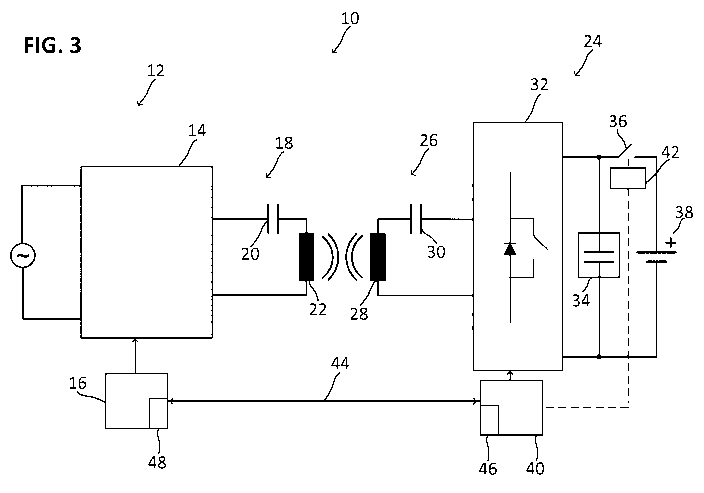
Fig. 3 shows a schematic diagram of a wireless power transmission system 10
using series-
series compensation according to the present invention.
As shown in Fig. 3, the inductive power transfer system 10 has a stationary
side circuit 12
comprising a stationary side DC/AC converter 14, a stationary side controller
16, and a
stationary side resonant circuit 18 set up from with at least one stationary
side capacitor
20 and at least one stationary side transmitter coil 22.
CA 03106875 2021-01-19
WO 2020/020875
PCT/EP2019/069776
8
Operatively, the stationary side DC/AC converter 14 is adapted to excite the
stationary
side resonant circuit 18 for generation of an oscillating magnetic field
during wireless
power transmission. Further, operatively the stationary side controller 16 is
adapted to
measure the stationary side high frequency current and optionally the
stationary side high
frequency voltage for control of the primary side DC/AC converter 14. Still
further,
operatively the stationary side controller 16 optionally is adapted to measure
the amount
of power transmitted wirelessly from the stationary side circuit 12 to a
mobile side circuit
24 of the wireless power transmission system 10.
As shown in Fig. 3, the wireless power transfer system 10 also has at least
one mobile side
circuit 24 separated from the stationary side circuit 12.
As shown in Fig. 3, the mobile side circuit 24 comprises a mobile side
resonant circuit 26
set up from at least one a receiver coil 28 connected in series to at least
one mobile side
capacitor 30. The mobile side circuit 24 further comprises a mobile side
rectifier 32. At the
input the mobile side rectifier 32 is connected to the mobile side resonant
circuit 26 and
at the output the mobile side rectifier 32 is connected to an energy storage
circuit 34. The
energy storage circuit 34, e.g., a capacitor, is connected via a switch 36 to
a load 38. The
mobile side circuit 24 comprises a mobile side controller 40 adapted to
control the mobile
side rectifier 32.
As shown in Fig. 3, the mobile side circuit may also comprise a mobile side
failure detector
42 adapted to detect occurrence of a failure state at the mobile side circuit
24 and
coupled to the mobile side controller 40. Optionally, the mobile side
controller 40 may
comprise a mobile side communication interface 46 adapted to indicate the
occurrence of
a failure sate to the stationary side controller 16.
Operatively, the receiver coil 28, when placed in the magnetic field produced
by the
transmitter coil 22, receives energy transmitted by the transmitter coil 22
through
inductive coupling. The inductive coupling leads to generation of a mobile
side high
frequency voltage and a mobile side high frequency current in the mobile side
resonant
circuit 26.
CA 03106875 2021-01-19
WO 2020/020875
PCT/EP2019/069776
9
Operatively, the mobile side rectifier 32 is adapted to convert the mobile
side high
frequency voltage and the mobile side high frequency current into a mobile
side rectified
voltage under control of the mobile side controller 40 for subsequent
smoothing by the
energy storage circuit 34. Also, operatively the mobile side rectifier 32
outputs a mobile
side direct current for supply to the load 38 across the switch 36.
Operatively, the mobile side controller 40 may be adapted to measure the
mobile side
high frequency current and to measure the mobile side high frequency voltage
as input to
the mobile side rectifier 32, as an option. Further, the mobile side
controller 40 is adapted
to measure the mobile side direct current and/or the mobile side DC voltage
and to
process generated measurement results for control of the mobile side rectifier
32.
As shown in Fig. 3, according to the present invention the provision of a
wireless
communication link 44 between the stationary side circuit 12 and the mobile
side circuit
24 is an option. In this case, the stationary side controller 16 comprises a
first
communication interface 48 and the mobile side controller 40 comprises a
second
communication interface 46. It should be noted that according to the present
invention
there no restriction regarding the type of wireless communication implemented
for the
wireless communication link 44 which may rely, e.g., on the IrDa standard, or
alternatively
on Bluetooth WiFi, WLAN, etc.
Generally, very often rectifiers on the mobile side of a wireless power
transmission system
use full- or half-bridge rectifiers set up from at least two rectifying
element, e.g., diodes or
active switching elements controlled by the mobile side controller 40 to
implement the
rectifying functionality.
In the most general sense according to the present invention it is suggest to
provide the
option to bypass or short circuit at least rectifying element in the mobile
side rectifier 32
upon occurrence of a failure. As will be explained in more detail in the
following this
allows to change the operative mode of the mobile side rectifier 32 to one
operative
mode selected from a group comprising:
= a half-bridge mode;
= a full-bridge mode;
CA 03106875 2021-01-19
WO 2020/020875
PCT/EP2019/069776
= a DC mode without polarity reversion where the voltage across the energy
storage
circuit 34 is switched through to the input side of the mobile side rectifier
32
without reversion of polarity of the voltage across the energy storage circuit
34;
= a DC mode with polarity reversion where the voltage across the energy
storage
5
circuit 34 is switched through to the input side of the mobile side rectifier
32 with
reversion of polarity of the voltage across the energy storage circuit 34;
= an antiphase mode where the input voltage and the input current of the
mobile
side rectifier 32 are phase-shifted with respect to each other according to a
predetermined range of phase-shift, e.g., by mapping the voltage across the
10 energy
storage circuit 34 to the input side of the mobile side rectifier while
maintain voltage polarity when the current flowing through the mobile side
resonant circuit 26 has negative polarity and by mapping the voltage across
the
energy storage circuit 34 to the input side of the mobile side rectifier while
reversing voltage polarity when the current flowing through the mobile side
resonant circuit 26 has positive polarity.
In the most general sense the change of operation mode in the mobile side
rectifier 32
changes the output power of the mobile side rectifier 32 to reduce the stress
and avoid
damage to the mobile side circuit. E.g., a transition from full-bridge mode to
half-bridge
mode suddenly reduces the output power by half. According to the present
invention, this
event can be detected on the stationary side to interrupt wireless power
transmission
from the stationary side circuit to the mobile side circuit.
An important advantage of the present invention is that the provision of a
communication
channel between the stationary side circuit and the mobile side circuit to
communicate
occurrence of a failure with time delays is not mandatory. To the contrary,
the present
invention enables immediate action by the mobile side circuit to handle an
occurrence of
a failure without time delay.
Further, while a person skilled in the art would suggest that making a short
circuit of the
secondary side resonant circuit 26 is safer than switching from a full-bridge
mode to a
half-bridge mode such understanding neglects that very high currents are
generated
CA 03106875 2021-01-19
WO 2020/020875
PCT/EP2019/069776
11
during this switching event leading to a new sort of danger. The present
invention
overcomes this danger.
Further, according to the present invention current stresses in the mobile
side rectifier 32
are significantly reduced upon occurrence of a failure due to the fact that
the change in
voltage is not as large as it is in the case of switching a hard short-
circuit.
Another important advantage according to the present invention is that for
change of the
operative mode of the mobile side rectifier in a minimum configuration only
one switching
element is needed to bypass or short circuit at least rectifying element in
the mobile side
rectifier 32 upon occurrence of a failure instead of two switches. This
reduces costs and
complexity of the system.
Further, it should be noted that according to the change of operative mode in
the mobile
.. side rectifier 32 is not restricted in any way and in to one direction
only, e.g. from full-
bridge mode to half-bridge mode, as long as the operative mode during failure-
free
operation is different from the target operative mode of the mobile side
rectifier 32 used
upon occurrence of a failure at the mobile side circuit 24.
In the following different examples for realizing the basic concept of the
present invention
as outlined above will be explained with reference to Fig. 4 to Fig. 19.
Fig. 4 shows a flowchart of operation for the mobile side circuit of the
wireless power
transmission system according to the present invention.
As shown in Fig. 4, in a step S10, operatively executed by the stationary side
circuit 12
under control of the stationary side controller 16 and by the mobile side
circuit 24 under
control of the mobile side controller 40, the wireless power transmission
system 10 starts
the wireless power transmission. At this stage, in a step S12, operatively
executed by the
mobile side failure detector 42 and the mobile side controller 40, it will be
checked
whether a failure occurs at the mobile side. If so, the failure handling
procedure according
to the present invention will start and otherwise the process flow proceeds
according to
standard procedure.
CA 03106875 2021-01-19
WO 2020/020875
PCT/EP2019/069776
12
As shown in Fig. 4, in a step S14, operatively executed by the mobile side
controller 40,
there is determined a first operative mode for the mobile side rectifier 32
according to
prevailing operative conditions, e.g., type of load 38, power consumption by
the load 38,
etc. Then the mobile side rectifier operates in the first operative mode
being, e.g., a ha If-
bridge rectification mode or a full bridge rectification mode during failure
free operation
of the mobile side circuit;
As shown in Fig. 4, in a step S16, operatively executed by the mobile side
failure detector
42 and the mobile side controller 40, it will again be checked whether a
failure sate occurs
at the mobile side. Such a check may be implement according to a predetermined
interval,
upon issuance of a related control signal, or any other suitable condition.
As shown in Fig. 4, if the result of step S16 is that a failure state occurs
at the mobile side
then there follows a step S18, operatively executed by the mobile side
controller 40, to
determine the second operative mode which is different from the first
operative mode
and is selected from a group comprising a half-bridge mode, a full-bridge
mode, a DC
mode where the voltage across the energy storage circuit 34 is switched
through to the
input of mobile side rectifier 32 with or without polarity reversion, and an
antiphase mode
where the input voltage and the input current of the mobile side rectifier 32
are shifted
with respect to each other according to a predetermined range.
As shown in Fig. 4, in a step S20, operatively executed by the mobile side
controller 40,
the mobile side rectifier 32 is operated in the second operative mode. As
outlined above
and explained in more detail in the following this may be achieved by
controlling at least
one switching element connected in parallel to at least one rectifying element
of the
mobile side rectifier 32 to change the first operative mode of the mobile side
rectifier 32
to the second operative mode upon occurrence of the failure state in the
mobile side
circuit.
As shown in Fig. 4, in a step S22, operatively executed by the mobile side
failure detector
42 and the mobile side controller 40, it will be checked whether the failure
prevails at the
mobile side. Such a check may be implemented according to a predetermined
interval,
CA 03106875 2021-01-19
WO 2020/020875
PCT/EP2019/069776
13
upon issuance of a related control signal, or any other suitable condition. If
the result of
step 22 is negative the operation of the mobile side circuit in the second
operative mode
will continue and otherwise the procedure will continue with operation of the
mobile side
circuit 24 in the first operative mode.
It should be noted that according to the present invention the first operative
mode may
be kept constant, e.g., in full ¨bridge mode or half-bridge mode, or may
change from full ¨
bridge mode to half-bridge mode when the operative conditions during failure
free
operation of the mobile side require so.
Fig. 5 shows a flowchart of operation for the stationary side circuit of the
wireless power
transmission system according to the present invention.
As shown in Fig. 5 and assuming that the wireless power transmission has
started, in a
step S24, operatively being controlled by the stationary side controller 16,
wireless power
transfer takes place from the stationary side to the mobile side. Then in a
step S26,
operatively executed by the stationary side controller 16, the amount of power
transmitted to the mobile side will be monitored. It should be noted that such
monitoring
may be implemented at regular intervals, at change of operative conditions, or
under any
other suitable condition.
As shown in Fig. 5, in a step S28, operatively executed by the stationary side
controller 16,
it will be determined whether the change in the amount of transmission power
or current
exceeds a predetermined threshold or not. A typical range for the
predetermined
threshold according to the present invention may lie in the range of 5 % to 20
%. If the
evaluation in step S28 is affirmative, there follows a step S30, operatively
executed by the
stationary side controller 16, to interrupt wireless power transmission to the
mobile side.
The interruption of power supply to the mobile side circuit 24 allows to avoid
any damage
to circuit elements of the mobile side circuit 24 in a very efficient and safe
manner.
As shown in Fig. 5 and as an option, if the evaluation in Step S28 is not
affirmative,
another way to achieve interruption of the power supply to the mobile side
circuit 24 is
the exchange of a notification of failure state from the mobile side circuit
to the stationary
CA 03106875 2021-01-19
WO 2020/020875
PCT/EP2019/069776
14
side circuit in a step 32, operatively executed by the mobile side controller
40 and the
mobile side communication interface 46 as well as the stationary side
controller 16 and
the stationary side communication interface 48.
In the following different examples for change of operative mode in the mobile
side
rectifier 32, according to a first embodiment of the present invention will be
explained
assuming the mobile side rectifier has a full-bridge circuit topology.
Fig. 6 shows a first example for change of the operative mode of the mobile
side rectifier
32 from a full-bridge mode to a half-bridge mode and vice versa according to a
first
embodiment of the present invention.
As shown in Fig. 6, the mobile side rectifier 32 is a full-bridge rectifier
and has a first
rectifying element 50 and a second rectifying element 52 connected in series
between a
first output terminal 54 and a second output terminal 56 of the full-bridge
rectifier and
having a common connection terminal connected to a first input terminal 58 of
the full-
bridge rectifier.
As shown in Fig. 6, the mobile side rectifier 32 further has a third
rectifying element 60
and a fourth rectifying element 62 connected in series between the first
output terminal
54 and the second output terminal 56 of the full-bridge rectifier 32 and
having a common
connection terminal connected to a second input terminal 64 of the full-bridge
rectifier.
As shown in Fig. 6, the mobile side rectifier further has a first switching
element 66 which
is connected in parallel to the first rectifying element 50.
As shown in Fig. 6, assuming that the first rectifying element 50 is bypassed
upon
occurrence of a failure state in the mobile side circuit 32, then, during a
positive half-cycle
of the input current to the mobile side rectifier 32, the current flows as
shown in the
middle illustration of Fig. 6, while during a negative half-cycle of the input
current to the
mobile side rectifier 32 flows as shown in the right illustration of Fig. 6.
CA 03106875 2021-01-19
WO 2020/020875
PCT/EP2019/069776
As shown in Fig. 6, during the positive half-cycle of the input current the
current flows
across the first switching element 66, the energy storage circuit 34 and the
fourth
rectifying element 62. Otherwise, during the negative half-cycle of the input
current the
current flows across the third rectifying element 60 and the first switching
element 66.
5
From the above it should be clear that by short circuiting or equivalently by-
passing the
first rectifying element 50 there is achieved a change of operative mode in
the mobile side
rectifier from full-bridge mode to half-bridge mode realizing a first half-
bridge circuit 68.
Also, a short circuit of the mobile side resonant circuit 26 and related
excessive transient
10 behavior of voltage and current at the mobile side circuit 24 may be
avoided as the
current will always flow across one rectifying element of the first half-
bridge circuit 68, the
first switching element 66 and ¨ during the positive half-cycle - the energy
storage circuit
34.
15 Fig. 7 shows a second example for change of operative mode of the mobile
side rectifier
from a full-bridge mode to a half-bridge mode and vice versa according to the
first
embodiment of the present invention.
The basic circuit topology for the mobile rectifier circuit 32 shown in Fig. 7
is similar to the
one outlined above with respect to Fig. 6, the difference being that a second
switching
element 70 is connected to the second rectifying element 52.
As shown in Fig. 7, assuming that the second rectifying element 52 is bypassed
upon
occurrence of a failure state in the mobile side circuit 32 then during a
positive half-cycle
of the input current to the mobile side rectifier 32 the current flows as
shown in the
middle illustration of Fig. 7, while during a negative half-cycle of the input
current to the
mobile side rectifier 32 flows as shown in the right illustration of Fig. 7.
As shown in Fig. 7, during the positive half-cycle of the input current the
current flows
across the second switching element 70 and the fourth rectifying element 62.
Otherwise,
during the negative half-cycle of the input current the current flows across
the third
rectifying element 60 and the energy storage circuit 34, and the second
switching element
70.
CA 03106875 2021-01-19
WO 2020/020875
PCT/EP2019/069776
16
From the above, it should be clear that by short circuiting or equivalently by-
passing the
second rectifying element 52 there is achieved a change of operative mode in
the mobile
side rectifier from full-bridge mode to half-bridge mode realizing a second
half-bridge
circuit 72. Further, the effects achieved according to the example shown in
Fig. 7 are the
same as explained above with respect to Fig. 6.
Fig. 8 shows a third example for change of operative mode of the mobile side
rectifier
from a full-bridge mode to a half-bridge mode and vice versa according to the
first
embodiment of the present invention.
The basic circuit topology for the mobile rectifier circuit 32 shown in Fig. 8
is similar to the
one outlined above with respect to Fig. 6, the difference being that a third
switching
element 74 is connected to the third rectifying element 60.
As shown in Fig. 8, assuming that the third rectifying element 60 is bypassed
upon
occurrence of a failure state in the mobile side circuit 32 then during a
positive half-cycle
of the input current to the mobile side rectifier 32 the current flows as
shown in the
middle illustration of Fig. 8, while during a negative half-cycle of the input
current to the
mobile side rectifier 32 flows as shown in the right illustration of Fig. 8.
As shown in Fig. 8, during the positive half-cycle of the input current the
current flows
across the first rectifying element 50 and the third switching element 74.
Otherwise,
during the negative half-cycle of the input current the current flows across
the third
switching element 74, the energy storage circuit 34, and the second rectifying
element 52.
From the above it should be clear that by short circuiting or equivalently by-
passing the
third rectifying element 60 there is achieved a change of operative mode in
the mobile
side rectifier from full-bridge mode to half-bridge mode realizing a third
half bridge circuit
76. Further, the effects achieved according to the example shown In Fig. 8 are
the same as
explained above with respect to Fig. 6.
CA 03106875 2021-01-19
WO 2020/020875
PCT/EP2019/069776
17
Fig. 9 shows a fourth example for change of operative mode of the mobile side
rectifier
from a full-bridge mode to a half-bridge mode and vice versa according to the
first
embodiment of the present invention.
The basic circuit topology for the rectifier circuit shown in Fig. 9 is
similar to the one
outlined above with respect to Fig. 6, the difference being that a fourth
switching element
78 is connected to the fourth rectifying element 62.
As shown in Fig. 9, assuming that the fourth rectifying element 62 is bypassed
upon
occurrence of a failure state in the mobile side circuit 32 then during a
positive half-cycle
of the input current to the mobile side rectifier 32 the current flows as
shown in the
middle illustration of Fig. 9, while during a negative half-cycle of the input
current to the
mobile side rectifier 32 flows as shown in the right illustration of Fig. 9.
As shown in Fig. 9, during the positive half-cycle of the input current the
current flows
across the first rectifying element 50, the energy storing unit 34 and the
fourth switching
element 78. Otherwise, during the negative half-cycle of the input current the
current
flows across the fourth switching element 78 and the second rectifying element
52.
From the above, it should be clear that by short circuiting or equivalently by-
passing the
fourth rectifying element 62 there is achieved a change of operative mode in
the mobile
side rectifier from full-bridge mode to half-bridge mode realizing a fourth
half bridge
circuit 80. Further, the effects achieved according to the example shown In
Fig. 8 are the
same as explained above with respect to Fig. 6.
Fig. 10 shows a signal diagram for voltage and current at the stationary side
circuit 12 and
the mobile side circuit 24 upon change of operative mode of the mobile side
rectifier from
a full-bridge mode to a half-bridge mode and vice versa according to the first
embodiment
of the present invention.
As shown in Fig. 10, compared to the constellation shown in Fig. 2 according
to the
present invention the transient behavior of voltage and current shows
significantly
reduced overshoot and thus achieves a related reduced load on the circuit
elements of the
CA 03106875 2021-01-19
WO 2020/020875
PCT/EP2019/069776
18
mobile side circuit 24. As shown in Fig. 10, current stresses in the mobile
rectifier circuit
32 are avoidable compared to the hard short circuit scenario as neither high
currents nor
high voltages are generated.
Fig. 11 shows a signal diagram for voltage and current at the stationary side
circuit 12 and
the mobile side circuit 24 upon change of operative mode of the mobile side
rectifier 32
from a half-bridge mode to a full-bridge mode and vice versa according to the
first
embodiment of the present invention.
As shown in Fig. 11, the present invention leads to similar results as shown
in Fig. 10 when
a change of operation mode for the mobile resonant circuit 32 is from a half-
bridge mode
to a full-bridge mode.
Further, the example shown in Fig. 11 is related to the scenario illustrated
above with
respect to Fig. 5 where the stationary side controller 16 detects increase of
power supply
to the mobile side circuit 32 or receives a notification of failure occurrence
at the mobile
side circuit 32 to then interrupt wireless power transfer to the mobile side
circuit 32.
In the following different examples for change of operative mode in the mobile
side
rectifier 32 according to a second embodiment of the present invention will be
explained
assuming that the mobile side rectifier has a full-bridge circuit topology.
The difference
with respect to the examples illustrated above with respect to Fig. 6 to Fig.
10 is that in
the examples to follow there are provided two switching elements for change of
operative
mode of the mobile side rectifier 32.
Fig. 12 shows a first example for change of the operative mode of the mobile
side rectifier
32 from a full-bridge mode to a DC mode without polarity reversion and vice
versa
according to a second embodiment of the present invention.
As shown in Fig. 12, the mobile side rectifier 32 comprises one switching
element 82
connected in parallel to the first rectifying element 50 and one switching
element 84
connected in parallel to the fourth rectifying element 62.
CA 03106875 2021-01-19
WO 2020/020875
PCT/EP2019/069776
19
Operatively, the mobile side control circuit 40 is adapted to close or open
simultaneously
the switching element 82 connected in parallel to the first rectifying element
50 and the
switching element 84 connected in parallel to the fourth rectifying element 62
upon
occurrence of a failure state in the mobile side circuit 32.
As shown in Fig. 12, assuming that the first rectifying element 50 and the
fourth rectifying
element 62 are bypassed upon occurrence of a failure state in the mobile side
circuit 32
then during a positive half-cycle of the input current to the mobile side
rectifier 32 the
current flows as shown in the middle illustration of Fig. 12, while during a
negative half-
cycle of the input current to the mobile side rectifier 32 flows as shown in
the right
illustration of Fig. 12.
As shown in Fig. 12, during the positive half-cycle of the input current the
current flows
across the switching element 82 connected in parallel to the first rectifying
element 50,
the energy storage circuit 34, and the switching element 84 connected in
parallel to the
fourth rectifying element 50. Further, during the negative half-cycle of the
input current
the current flows across the switching element 84 connected in parallel to the
fourth
rectifying element 62, the energy storage circuit 34, and the switching
element 82
connected in parallel to the first rectifying element 50.
Fig. 13 shows an equivalent schematic diagram for the change of the operative
mode of
the mobile side rectifier from a full-bridge mode to a DC mode without
polarity reversion
as shown in Fig. 12.
As shown in Fig. 13, to change the second operative mode to the DC-mode
without
polarity reversal of the voltage across the energy storage circuit 34. By
switching on both
switching elements 82 and 84 the power transfer to the load 38 is interrupted
immediately. The secondary resonant circuit is connected to a DC-voltage which
is equal
to the voltage of the energy storage circuit 34. Optionally, the stationary
side circuit 12 of
the wireless power transmission system detects this event and shuts down the
power
supply of the from the stationary side circuit 12 to the mobile side circuit
24.
CA 03106875 2021-01-19
WO 2020/020875
PCT/EP2019/069776
Fig. 14 shows a second example for change of the operative mode of the mobile
side
rectifier from a full-bridge mode to a DC mode with polarity reversion and
vice versa
according to the second embodiment of the present invention.
5 As
shown in Fig. 14, the mobile side rectifier 32 comprises one switching element
86
connected in parallel to the second rectifying element 52 and one switching
element 88
connected in parallel to the third rectifying element 60.
Operatively, the mobile side control circuit 40 is adapted to close or open
simultaneously
10 the
switching element 86 connected in parallel to the second rectifying element 52
and
the switching element 88 connected in parallel to the third rectifying element
60 upon
occurrence of a failure state in the mobile side circuit 32.
As shown in Fig. 14, assuming that the second rectifying element 52 and the
third
15
rectifying element 60 are bypassed upon occurrence of a failure state in the
mobile side
circuit 32 then during a positive half-cycle of the input current to the
mobile side rectifier
32 the current flows as shown in the middle illustration of Fig. 14, while
during a negative
half-cycle of the input current to the mobile side rectifier 32 flows as shown
in the right
illustration of Fig. 14.
As shown in Fig. 14, during the positive half-cycle of the input current the
current flows
across the switching element 86 connected in parallel to the second rectifying
element 52,
the energy storage circuit 34, and the switching element 88 connected in
parallel to the
third rectifying element 60. Further, during the negative half-cycle of the
input current the
current flows across the switching element 88 connected in parallel to the
third rectifying
element 60, the energy storage circuit 34, and the switching element 86
connected in
parallel to the second rectifying element 52.
Fig. 15 shows an equivalent schematic diagram for the change of the operative
mode of
the mobile side rectifier from a full-bridge mode to a DC mode with polarity
reversion as
shown in Fig. 14.
CA 03106875 2021-01-19
WO 2020/020875
PCT/EP2019/069776
21
As shown in Fig. 15, the difference between the first example of the second
embodiment
of the present invention explained above with respect to Fig. 12 and Fig. 13
and the
second example of the second embodiment of the present invention explained
with
respect to Fig. 13 and Fig. 14 is a DC mode where the voltage across the
energy storage
circuit 34 is mapped to the input terminals of the rectifier circuit 32 with
polarity reversal.
Also, here, the mobile side resonant circuit 26 is never short circuited so
that similar
effects as outlined above for the first example of the second embodiment of
the present
invention may be achieved for the second example of the second embodiment of
the
present invention.
In the following, different examples for change of operative mode in the
mobile side
rectifier 32 according to a third embodiment of the present invention will be
explained
assuming that the mobile side rectifier has a full-bridge circuit topology.
The difference
with respect to the examples illustrated above with respect to Fig. 6 to Fig.
10 is that in
the examples to follow there are provided four switching elements for change
of
operative mode of the mobile side rectifier 32.
Fig. 16 shows an example for change of the operative mode of the mobile side
rectifier 32
from a full-bridge mode to an antiphase mode and vice versa according to a
third
embodiment of the present invention.
As shown in Fig. 16, according to the third embodiment of the resent invention
the mobile
side rectifier 32 has one switching element 90 connected in parallel to the
first rectifying
element 50, one switching element 92 connected in parallel to the second
rectifying
element 52, one switching element 94 connected in parallel to the third
rectifying element
60, and one switching element 96 connected in parallel to the fourth
rectifying element
62.
Operatively, the mobile side control circuit 40 is adapted to implement the
antiphase
mode by simultaneously closing the switching element 90 connected in parallel
to the first
rectifying element 50 and the switching element 96 connected in parallel to
the fourth
rectifying element 62 and opening the switching element 92 connected in
parallel to the
second rectifying element 52 and the switching element 94 connected in
parallel the third
CA 03106875 2021-01-19
WO 2020/020875
PCT/EP2019/069776
22
rectifying element 60 during a negative cycle of the current from the mobile
side resonant
circuit 26.
Further, operatively, the mobile side control circuit 40 is adapted to
implement the
antiphase mode by simultaneously closing the switching element 92 connected in
parallel
to the second rectifying element 52 and the switching element 94 connected in
parallel to
the third rectifying element 60 and opening the switching element 90 connected
in
parallel to the first rectifying element 50 and the switching element 96
connected in
parallel to the fourth rectifying element 62 during a positive cycle of the
current from the
mobile side resonant circuit 26.
As shown in Fig. 16, assuming that the first rectifying element 50 and the
fourth rectifying
element 62 are bypassed upon occurrence of a failure state in the mobile side
circuit 32
then during a negative half-cycle of the input current to the mobile side
rectifier 32 the
current flows as shown in the middle illustration of Fig. 16 while during a
positive half-
cycle of the input current to the mobile side rectifier 32 flows as shown in
the right
illustration of Fig. 16.
As shown in Fig. 16, during the negative half-cycle of the input current the
current flows
across the switching element 92 connected in parallel to the first rectifying
element 50,
the energy storage circuit 34, and the switching element 96 connected in
parallel to the
fourth rectifying element 62. Further, during the positive half-cycle of the
input current
the current flows across the switching element 94 connected in parallel to the
third
rectifying element 60, the energy storage circuit 34, and the switching
element 96
connected in parallel to the fourth rectifying element 62.
Fig. 17 shows an equivalent schematic diagram for the for change of the
operative mode
of the mobile side rectifier from a full-bridge mode to the antiphase mode as
shown in Fig.
16 for a negative cycle of the input current to the mobile side rectifier.
As shown in Fig. 17, in the case of occurrence of a failure state in the
mobile side circuit
32, the four switching elements 90, 92, 94, 96 create a voltage u_2,hf which
has a 180'
phase shift in comparison to the current i_2,hf, i.e. create a positive
voltage u_2,hf during
CA 03106875 2021-01-19
WO 2020/020875
PCT/EP2019/069776
23
a negative half cycle of the current i_2,hf. Thus, energy will be transferred
back to the
stationary side where the stationary side controller 15 may detect this event
and shut
down the supply of power the stationary side resonant circuit 26 and thus also
to the
mobile side circuit 24.
Fig. 18 shows an equivalent schematic diagram for the change of the operative
mode of
the mobile side rectifier from a full-bridge mode to the antiphase mode as
shown in Fig.
16 for a positive cycle of the input current to the mobile side rectifier.
As shown in Fig. 18, in the case of occurrence of a failure state in the
mobile side circuit
32, the four switching elements 90, 92, 94, 96 create a voltage u_2,hf which
has a 1800
phase shift in comparison to the current i_2,hf, i.e. create a negative
voltage u_2,hf during
a positive half cycle of the current i_2,hf. Thus, also during the positive
half cycle of the
current i_2,hf energy will be transferred back to the stationary side. Again,
the stationary
side controller 16 may shut down the supply of power to the mobile side
circuit 24.
It should be noted that according to the present invention the phase shift
between the
voltage u_2,hf and the current i_2,hf is not restricted to a value of 180 .
Generally,
according to the present invention the mobile side controller 40 may be
adapted to
control the switching elements 90, 92, 94, 96 to create a voltage u_2,hf which
has a phase
shift in comparison to the current i_2,hf which lies in the range of 180 30 .
As an
alternative the phase shift may lie in the range of 90 30 which leads to a
reduced power
transfer to the mobile side circuit while at the same time reducing the stress
on related
circuit elements compared to the range of 180 30 .
In the following an example for change of operative mode in the mobile side
rectifier 32
according to a fourth embodiment of the present invention will be explained
assuming the
mobile side rectifier has a half-bridge circuit topology.
Fig. 19 shows an example change of the operative mode of the mobile side
rectifier from a
half-bridge mode to the DC mode without polarity reversal and vice versa upon
occurrence of a failure at the mobile side according to a fourth embodiment of
the
present invention.
CA 03106875 2021-01-19
WO 2020/020875
PCT/EP2019/069776
24
As shown in Fig. 19, according to the fourth embodiment of the present
invention the
mobile side rectifier (32) is a half-bridge rectifier having a first
rectifying element 98 and a
second rectifying element 100 connected in series between a first output
terminal 102
.. and a second output terminal 104 of the half-bridge rectifier and having a
common
connection terminal connected to a first input terminal 106 of the half-bridge
rectifier and
having the connection terminal of the second rectifying element different from
the
common connection point connected to a second input terminal 108 of the half-
bridge
rectifier. Further, according to the fourth embodiment of the present
invention one
switching element 110 is connected in parallel to the first rectifying element
98.
According to the fourth embodiment, operatively the mobile side control
circuit 40 is
adapted to close the switching element 110 connected in parallel to the first
rectifying
element 98 to change the second operative mode to the DC mode without polarity
reversal of the voltage across the energy storage circuit 34.
As shown in Fig. 19, assuming that the first rectifying element 98 of the half-
bridge
rectifier is bypassed upon occurrence of a failure state in the mobile side
circuit 32 then
during a positive half-cycle of the input current to the mobile side rectifier
32 the current
flows as shown in the middle illustration of Fig. 19, while during a negative
half-cycle of
the input current to the mobile side rectifier 32 flows as shown in the right
illustration of
Fig. 19. I.e., in both case the current will flow across the switching element
110 and the
energy storage circuit 34, however, along different directions.