Note: Descriptions are shown in the official language in which they were submitted.
CA 03106887 2021-01-19
WO 2020/021029
PCT/EP2019/070082
Resonant cavity surface acoustic wave (SAW) filters
The invention relates to surface acoustic wave devices for filter applications
and, more
particularly, to a composite substrate for surface acoustic wave filter
devices.
In recent years, surface acoustic wave (SAW) devices have been employed in an
increasing number of practical applications, such as filters, sensors and
delay lines.
The synthesis of SAW filters requires different types of tools and allows for
different
types of structures to be implemented. However, the use of classical filter
structures in SAW
devices faces various problems, such as compactness and performance of the
device.
SAW filter devices commonly use wafers made from a monolithic Quartz, LiNb03
or
LiTa03 crystal as piezoelectric materials. However, the use of piezoelectric
substrates leads
to either high sensibility to temperature or weak electromechanical coupling
depending on the
piezoelectric material used. This results in poor performance of the filters'
pass-band
characteristics.
The filter performance is defined using several parameters such as bandwidth,
in-band
insertion loss, rejection and transition bandwidth, separating the passband
and the rejection
band.
Furthermore, the use of cavities for generating poles and zeros in filter
transfer function
is a well-known technique used systematically when developing microwave
filters operating at
several GHz. Such a filter requires a waveguide along which are disposed
resonant elements
yielding poles or zero depending the way they are connected one another (in
series or in
parallel). The synthesis of such filters is based on the combination of these
poles and zeros
providing reduced ripples in the band and an improved out-of-band rejection
assuming a given
coupling factor between the source and the filtering structure. In any case,
the filter only
consists in a series of cavities connected to one another or placed along the
said waveguide
and accessed either by an electric connector or directly via the edges of the
waveguide. For
SAW devices, a conversion has to be achieved from electromagnetic to acoustic
waves and
vice versa to provide the electromagnetic filtered signal. In between,
electrode structures are
combined in a way that resonance can be combined either electrically or
acoustically to
produce the filtering effects.
So far, presently developed solutions for SAW filters are using three kinds of
architectures to achieve the filter function, mainly impedance element
lattices (the so-called
SAW-ladder) or longitudinally coupled resonators filters (LCRF) or double-mode
SAW (DMS)
CA 03106887 2021-01-19
WO 2020/021029 2
PCT/EP2019/070082
filters both based on coupling IDTs using gratings operating close to the
Bragg condition.
However, these approaches generally allow for two or more poles to be placed
in the
passband, thus resulting in non-optimized performance of the device and need a
relatively
large footprint.
The object of the invention is to overcome the drawbacks cited previously by
providing
a surface acoustic wave (SAW) filter device deposited on a composite substrate
with improved
design for compactness, simplicity and versatility as well as good
performance.
The object of the invention is achieved by a coupled cavity filter structure,
using a
surface acoustic wave, in particular a guided surface acoustic wave,
comprising an
acoustic wave propagating substrate, at least one input transducer structure
and one output
transducer structure, provided over the substrate, each comprising inter-
digitated comb
electrodes, one reflecting structure, said reflecting structure comprising at
least one or more
metallic strips, positioned at a distance d and in between the input and
output transducer
structures, in the direction of propagation of an acoustic wave, characterised
in that the
acoustic wave propagation substrate is a composite substrate comprising a base
substrate
and a piezoelectric layer. With such a filter structure, the passband can be
adjusted and at the
same time filter structures with reduced footprint can be obtained compared to
the above
described filter structures in the art.
According to a variant of the invention, the coupled cavity filter structure
can be
configured so that the surface acoustic wave is a shear wave or a longitudinal
wave inside the
piezoelectric layer. Whereas in the prior art use was made of Rayleigh waves,
the use of a
piezoelectric layer instead of a bulk substrate opens the way to use acoustic
waves of a
different type, thereby providing further optimization parameters. Guided
shear waves can
provide the highest electromechanical coupling reachable using composite
substrates. They
allow for accessing higher wave velocities than elliptically polarized waves
with extended
opportunities for thermal compensation compared to classical Rayleigh-like
waves.
Furthermore, the use of given combination of substrates and excitation
conditions enables one
to excite longitudinally polarized guided waves, yielding higher velocity than
other wave types,
shear waved and Rayleigh wave, with coupling in excess of 5%.
According to a variant of the invention, the inter-digitated comb electrodes
of the at
least one input transducer structure and one output transducer structure can
be defined by the
Bragg condition given by p = A /2, A being the operating acoustic wavelength
of said transducer
structures and p being the electrode pitch of said transducer structures. This
approach enables
to yield optimal dimension and excitation conditions or coupling conditions
for given frequency,
bandwidth and energy confinement.
CA 03106887 2021-01-19
WO 2020/021029 3
PCT/EP2019/070082
According to a variant of the invention, the coupled cavity filter structure
can comprise
further at least one Bragg mirror, located apart the input and/or output
transducer structure, on
the opposite side of the side where the one reflecting structure is located,
in the direction of
propagation of the acoustic wave. The presence of the Bragg mirror located
next to the
.. transducer structure enables to reduce losses in the structure.
According to a variant of the invention, the coupled cavity filter structure
can comprise
a plurality of reflecting structures, separated from each other by a gap g and
positioned at a
distance d and in between with respect to the input and output transducer
structures, in the
direction of propagation of an acoustic wave, each gap g between the
reflecting structures and
each gap d between a transducer structure and its adjacent reflecting
structure forming an
acoustic cavity. The fact that the structure has more than one reflecting
structure provides a
plurality of acoustic cavities in the structure. A higher number of acoustic
cavities allows
narrowing the transition band.
According to a variant of the invention, the dimension of each acoustic cavity
of the
cavity filter structure can be smaller than A/4, in particular so that the
phase velocity in the
cavity is superior to the phase velocity within the reflecting structure. Such
dimensions can
improve the resonance conditions and thereby the performance of the filter.
According to a variant of the invention, the distance between neighbouring
reflecting
structures of the plurality of reflecting structures and / or the distance
between a reflecting
structure and a neighbouring transducer structure can be the same or
different. By adapting
the dimension of the gap, thus of the cavity, the filter parameters can be
improved.
According to a variant of the invention, the reflecting structure or the
reflecting
structures can have a unitary metallic strip reflection coefficient superior
to the coupling
coefficient ks2of the composite substrate and of the electrodes of the
transducer structure, in
particular a unitary metallic strip reflection coefficient at least 1.5 times
superior to the coupling
coefficient ks2. A higher ratio of the reflection coefficient over the
coupling coefficient provides,
for a given bandwidth, an essentially flat in-band transfer function and
sharpened transition
bands, with a reduced in-band ripple effect compared to filters not satisfying
the condition.
According to a variant of the invention, each reflecting structure can
comprise at least
.. one or more metallic strips with a pitch of the metallic strips being the
same or being different
to the electrode pitch of the transducer structure. Using highly reflecting
structures can give
more tolerance of the mirror to manufacturing variations but it also allows
for shifting reflection
function zeros to improve the out-band rejection.
CA 03106887 2021-01-19
WO 2020/021029 4
PCT/EP2019/070082
According to a variant of the invention, the metallic strips of each
reflecting structure can
be electrically connected to each other. Thus, a constant value of the
electrical potential
throughout each reflecting structure can be obtained, thereby improving the
reflection
coefficient of the reflecting structure at the Bragg condition.
According to a variant of the invention, the number of metallic strips of each
reflecting
structure of the plurality of reflecting structures can be below 30,
preferentially below 20, so
that the reflection coefficient of the plurality of reflecting structures is
above 0,5, in particular
above 0,8. Thus, the cavities confinement of the acoustic energy can be
improved and mode
coupling conditions can be provided in the structure.
According to a variant of the invention, the difference between the acoustic
impedance
of the material from the piezoelectric layer and the material from the
metallic strips of the
each reflecting structure of the plurality of reflecting structures can be
such that the reflection
coefficient of the plurality of reflecting structures is superior to 0,5, in
particular superior to 0,8.
By increasing the reflection coefficient, it becomes possible to reduce the
size of the filter
structure.
The object of the invention is also achieved by a coupled cavity filter
structure, using a
surface acoustic wave, in particular a guided surface acoustic wave,
comprising an
acoustic wave propagating substrate, at least one input transducer structure
and one output
transducer structure, provided over the substrate, each comprising electrodes,
one reflecting
structure, said reflecting structure comprising a groove, positioned at a
distance L and in
between the input and output transducer structures, in the direction of
propagation of an
acoustic wave, characterised in that the acoustic wave propagation substrate
is a composite
substrate comprising a base substrate and a piezoelectric layer. With such a
filter structure,
the passband can be adjusted and at the same time filter structures with
reduced footprint can
be obtained compared to the above described filter structures in the art.
According to a variant of the invention, the coupled cavity filter structure
can be
configured so that the surface acoustic wave is a shear wave or a longitudinal
wave inside the
piezoelectric layer. Whereas in the prior art use was made of Rayleigh waves,
the use of a
piezoelectric layer instead of a bulk substrate opens the way to use acoustic
waves of a
different type, thereby providing further optimization parameters. Guided
shear waves can
provide the highest electromechanical coupling reachable using composite
substrates. They
allow for accessing higher wave velocities than elliptically polarized waves
with extended
opportunities for thermal compensation compared to classical Rayleigh-like
waves.
Furthermore, the use of given combination of substrates and excitation
conditions enables one
to excite longitudinally polarized guided waves, yielding higher velocity than
other wave types,
CA 03106887 2021-01-19
WO 2020/021029 5
PCT/EP2019/070082
shear waved and Rayleigh wave, with coupling in excess of 5%.
According to a variant of the invention, the coupled cavity filter structure
can comprise
further at least one additional groove, located apart the input and/or output
transducer structure
on the opposite side of the side where the one reflecting structure is
located, in the direction
of propagation of the acoustic wave. The presence of the grooves located next
to the
transducer structure enables to reduce losses in the structure and can be
configured such as
to obtain a total reflection of the acoustic wave propagating in the
transducer.
According to a variant, the electrodes of the at least one input transducer
structure and
one output transducer structure can be defined by the electrode pitch p being
equal to nA, A
being the operating acoustic wavelength of said transducer structures.
According to a variant, the coupled cavity filter structure can further
comprise at least
one additional groove, located apart the input and/or output transducer
structure on the
opposite side of the side where the one reflecting structure is located, in
the direction of
propagation of the acoustic wave.
According to a variant, the depth D3 of the at least one additional groove
located apart
the input and/or output transducer structure on the opposite side of the side
where the one
reflecting structure is located, in the direction of propagation of the
acoustic wave, can be of
the order of 2, or more.
According to a variant, the coupled cavity filter can comprise a plurality of
reflecting
structures separated from each other by a gap g and positioned at a distance L
and in between
the input and output transducer structures, in the direction of propagation of
an acoustic wave,
each gap g between the reflecting structures forming an acoustic cavity.
According to a variant,
the distance L2 between the edge of the groove and a position A, B in the
direction of
propagation of an acoustic wave corresponding to the end of the pitch of the
transducer
structure (812, 814) on the side where the groove is located can form an
acoustic cavity. The
fact that the structure has more than one reflecting structure provides a
plurality of acoustic
cavities in the structure. A higher number of acoustic cavities allows
narrowing the transition
band.
According to a variant, the distance between the edge of the groove (822,
1022, 1322,
1422, 1522, 1722) and the edge of the at least one additional groove (932,
934) can be of
the order of nA. Such dimensions can improve the resonance conditions and
thereby the
performance of the filter.
CA 03106887 2021-01-19
WO 2020/021029 6
PCT/EP2019/070082
According to a variant, the relief angle of the groove of the reflecting
structuree, the relief
angle being the angle between the horizontal axis X and the edge walls of the
groove, can be
of the order of 700 or more, in particular is of the order of 900.
According to a variant, the depth of the groove of the reflecting structuree
is of the order
of 2, or more, in particular is of the order of 102. or more, 2, being the
wavelength of the surface
acoustic wave.
According to a variant, the at least one additional groove is configured such
as to obtain
a total reflection of the propagating wave along the propagation direction.
According to a variant, the acoustic cavity formed between at least two
grooves of the
plurality of reflecting structures can be located at the surface of the
substrate, being also the
surface of the substrate where the transducer are located.
According to a variant, the acoustic cavity formed between at least two
grooves of
the plurality of reflecting structures can be located at a depth comprised
between the surface
of the substrate and the bottom surface of the at least two grooves located at
a depth D.
According to a variant, the input and output transducer structures can be
different, in
particular, the number of electrodes fingers of each transducer structure can
be different. Thus,
the filter structure is more versatile and the structure of the transducer can
be modified in order
to optimize the coupling efficiency of the mode within the reflecting
structures in order to obtain
low insertion loss.
According to a variant of the invention, the acoustic cavities can be split
into sub-
cavities separated from one another. The sub-cavities can be separated from
one another by
additional layers allowing for generating evanescent coupling from one cavity
to another. Thus,
the sub-cavities favor energy confinement in the structure and can lead to an
improvement of
the compactness of the device.
According to a variant of the invention, the cavity filter structure comprises
at least three
or more transducer structures in the direction of propagation of the acoustic
wave. The source
density can be increased, yielding an improved rejection. Also the filter band
can be flatter than
for the same filter with only two transducers.
According to a variant of the invention, the characteristics of the
piezoelectric layer
and of the electrodes of the transducer structures can be chosen such that the
CA 03106887 2021-01-19
WO 2020/021029 7
PCT/EP2019/070082
electromechanical coupling coefficient ks2 of the shear wave, preferentially
guided or
guided longitudinal wave in the piezoelectric layer is superior to 5%, in
particular superior
to 7% to obtain a higher filter bandpass properties, in particular by adapting
the electrode
geometry of transducer structure, e.g. the thickness, width and/or length
and/or number and/or
shape of the electrodes but also the thickness of the piezoelectric layer
which should be larger
than or equal to 5% of the wavelength A.
According to a variant of the invention, the thickness of the piezoelectric
layer can be
chosen such that the electromechanical coupling coefficient ks2 of the shear
wave,
preferentially guided, or of the guided longitudinal wave, in the
piezoelectric layer (104) is
superior to 5%, in particular superior to 7%. For a larger thickness, larger
than A, the acoustic
wave loses its guided property yielding multiple wave emission in the layer
and energy losses
in the substrate.
According to a variant of the invention, the cavity filter structure can
further comprise a
dielectric layer, in particular a SiO2 layer, sandwiched between the base
substrate and the
piezoelectric layer. The dielectric or passivation layer can improve the
attachment of the
piezoelectric layer over the base substrate but can also improve the
electromechanical
coupling while keeping temperature stability of the surface acoustic wave
device. Preferably,
the dielectric layer has a thickness of less than 1pm, in particular a
thickness in a range of
100nm to 1pm.
According to a variant of the invention, the piezoelectric layer of the
composite
substrate can be Aluminium Nitride (AIN), Zinc Oxide (Zn0), PZT, Niobate
Potassium KNb03
and similar materials such as KTN, etc., as well as piezolectric relaxors such
as PMN-PT and
related materials, Gallium Nitride (GaN), Lithium Tantalate LiTa03 or Lithium
Niobate LiNb03
with a crystallographic orientation for Lithium Tantalate LiTa03 or Lithium
Niobate LiNb03
defined as (YX/)/0 according to the standard IEEE 1949 Std-176, with 0, an
angle of the
crystallographic orientation being comprised between 0 and 60 or between 90
and 1500.
According to a variant of the invention, the base substrate of the composite
substrate
can be one of Silicon, in particular a high resistivity Silicon substrate
comprising a trap-rich
layer, Carbon-Diamond, Sapphire, or Silicon-Carbide. By high resistivity, one
understands
electrical resistivity of more than 1000 Ohm.cm. For transferring
piezoelectric layers on Silicon,
mass production methods like SmartCutTM, using ion implantation in a
piezoelectric source
substrate to define a layer to be transferred, attaching the source substrate
to a Silicon
substrate and transferring the layer by a thermal or mechanical treatment can
be used.
Simpler approaches based on bonding a piezoelectric substrate to the base
substrate with
subsequent thinning (via CMP, grinding, polishing) of the piezoelectric
substrate may also be
CA 03106887 2021-01-19
WO 2020/021029 8
PCT/EP2019/070082
used for the present invention, in particular suitable for thick piezoelectric
layers envisaged of
the order of a final thickness of 5 to 20 pm. Both approaches, layer transfer
via SmartCutTm or
via bonding/thinning, lead to single crystal piezoelectric layers formed on
the base substrate,
having thus high quality.
According to a variant of the invention, the base substrate can comprise a
Bragg mirror,
underneath the piezoelectric layer. The Bragg mirror consists of a stack of
layers with
periodically alternated acoustic impedance deposited or manufactured on top of
a plate of any
inorganic material. The said stack of layers behaves like a mirror for the
waves excited in the
top piezoelectric layer provided the thickness of each layer is about a
quarter of the acoustic
wavelength. Therefore, the mirror reflects waves with components pointing
toward the
substrate depth, confining the waves in the piezoelectric layer.
According to a variant of the invention, the coupled cavity surface acoustic
wave filter
structure has a filter band-pass comprised between 0.5% and 10%. It is
possible to vary the
bandpass of the filter device by varying the parameters of the cavity filter
structure and thus
the device can be adapted to the specifications of a user to obtain the
required filter bandpass.
According to a variant of the invention, the coupled cavity filter structure
can further
comprise a passivation layer formed over the transducer structures and the at
least one
reflecting structures, the passivation layer having a predetermined thickness
which is same or
different over the transducer structures and/or the at least one reflecting
structures.
The object of the invention is also achieved with a SAW ladder filter device
comprising
at least two coupled cavity filter as described previously, wherein the at
least two coupled
cavity filter devices can be positioned on a single line. Since the coupled
cavity filters according
to the invention can be positioned on a single line, the positioning and
connecting of the
multiple cavity filters does not require so much space as in state of the art
SAW ladder device.
The SAW ladder filter device according to the invention consists in a
compacter device
compared to a state of the art SAW ladder filter device.
The invention may be understood by reference to the following description
taken in conjunction
with the accompanying figures, in which reference numerals identify features
of the invention.
Figures la and lb illustrate a coupled cavity surface acoustic wave filter
structure according
to a first embodiment of the invention and its variants.
Figures 2a to 2e illustrate a coupled cavity surface acoustic wave filter
structure according to
a second embodiment of the invention and its variants.
CA 03106887 2021-01-19
WO 2020/021029 9
PCT/EP2019/070082
Figures 3a to 3d show the performance of a coupled cavity surface acoustic
wave filter
structure as shown in Figure 2b, with a composite substrate according to the
invention, with a
SiO2 layer of 500nm in between a LiTa03 (YX/)/42 piezoelectric layer of 6pm
and a semi-
infinite (100) Silicon substrate.
Figure 4 shows a table listing the characteristics of the coupled cavity
surface acoustic wave
filter structure as shown in Figure 2b, according to the invention.
Figures 5a and 5b illustrate a coupled cavity surface acoustic wave filter
structure according
to a third embodiment of the invention.
Figure 6 illustrates a coupled cavity surface acoustic wave filter structure
according to a fourth
.. embodiment of the invention.
Figure 7 illustrates a coupled cavity surface acoustic wave filter structure
according to a fifth
embodiment of the invention.
Figures 8a to 8h illustrate a coupled cavity surface acoustic wave filter
structure according to
a sixth embodiment of the invention and its variants.
Figure 9 shows the device according to the third embodiment of the invention
used for a
practical example of a simulation.
Figures 10a and 10b show the simulated characteristics of the coupled cavity
surface acoustic
wave filter structure as shown in Figure 9, according to the third embodiment
of the invention.
Figures 11a to 11d show the influence of parameters of the device on the
simulated
characteristics of a coupled cavity surface acoustic wave filter structure as
shown in Figure 9,
according to the third embodiment of the invention.
Figures 12a and 12b illustrate an example of a SAW ladder filter device
according to the state
of the art in Figure 12a and according to the invention in Figure 12b.
Figure 1 shows a coupled cavity surface acoustic wave filter structure
according to a
first embodiment of the invention. In Figure la, the coupled cavity surface
acoustic wave filter
structure 100 is realized on a substrate 102, being a composite substrate. The
composite
substrate 102 comprises a layer of piezoelectric material 104, with
crystallographic axis X, Y
and Z, formed over a base substrate 106.
The piezoelectric layer 104 in this embodiment is LiTa03 or LiNb03,
particularly with
cut orientations defined by (YX/)/0 according to the standard IEEE 1949 Std-
176, with 0, an
angle of the crystallographic orientation being comprised between 0 and 60
or between 90
CA 03106887 2021-01-19
WO 2020/021029 1 0
PCT/EP2019/070082
and 1500, Potassium Niobate KNb03 and similar material composition such as
KTN, as well
as other piezoelectric layers using sputtered or epitaxial films, for instance
Aluminium Nitride
AIN, Zinc Oxide ZnO, PZT, GaN or any composition of AIN and GaN.
The thickness of the piezoelectric layer 104 formed on the base substrate 106
is of the
order of one wavelength A or smaller, in particular is of about 20 pm or less.
The thickness t of
the base substrate 106 is larger than the thickness of the piezoelectric layer
104. A preferred
situation corresponds to a base substrate thickness that is at least ten times
larger than the
thickness of the piezoelectric layer 104, in particular 50 to 100 times
larger, which would
correspond to a base substrate thickness equal to 250 - 500pm.
The base substrate 106 used in the first embodiment of the invention is a
Silicon
substrate, in particular a high resistivity Silicon substrate. The orientation
of the Silicon
substrate is preferably (100) due to the higher acoustic wave propagation
velocity compared
to other crystalline orientation, such as for example (110), (111) or (001),
which can however
be used. Instead of Silicon, other substrate materials with an acoustic wave
propagation
velocity larger than the one of the piezoelectric layer can be chosen, such as
Carbon-Diamond,
Sapphire, or Silicon Carbide can be used.
In a variant of the invention, the base substrate 106 may further comprise a
so called
trap-rich layer close to the top layer of piezoelectric material, said trap-
rich layer improving the
isolation performance of the base substrate and may be formed by at least one
of
polycrystalline, amorphous, or porous materials such as for instance
polycrystalline Silicon,
amorphous Silicon, or porous Silicon, but the invention is not limited to such
materials.
In a variant of the invention, the base substrate 106 can further comprise a
Bragg
mirror, underneath the piezoelectric layer 104. The Bragg mirror consists of a
stack of layers
with periodically alternated acoustic impedance deposited or manufactured on
top of a plate
of any inorganic material. The acoustic impedance is the product of the wave
velocity times
the material density and is expressed in Rayleigh and preferably in Mrayleigh,
i.e. 106 Rayleigh.
A piezoelectric layer is deposited or manufactured atop the layer stack for
the excitation and
detection of acoustic waves. The stack may be advantageously composed of an
alternation of
Tungsten and Silica, or Si3N4 and 5i02, or Mo and Al, and in general any
couple of material
exhibiting an acoustic impedance ratio larger than two. The inorganic sub
plate may be
advantageously standard silicon or high resistivity silicon or glass and
generally any material
exhibiting a thermal coefficient of expansion (TCE) smaller than 6ppm/K. It
can also
incorporate a trap-rich layer to improve electrical isolation. Advantageously,
the first layer of
the stack can be 5i02 or in general any material that can be used to bound the
piezoelectric
layer to the above-described composite substrate.
CA 03106887 2021-01-19
WO 2020/021029 1 1
PCT/EP2019/070082
In this embodiment, a thin SiO2 layer 108 is provided at the interface 110
between the
piezoelectric layer 104 and the base substrate 106 to improve the attachment
of the
piezoelectric material layer 104 to the base substrate 106. The SiO2 layer 110
is 200nm thick,
but in a variant, the thickness of the SiO2 layer 110 can vary and be more or
less than 200nm
thick, in particular can vary between lOnm and 6pm.
The coupled cavity filter structure 100 comprises also two transducer
structures 112,
114 and one reflecting structure 116, positioned between the two transducer
structures 112,
114 at a certain distance d of the transducer structures 112, 114 in the
direction of propagation
X as shown in Figure 1. The region located between the reflecting structure
116 and one
.. transducer structure 112, 114, for example the region 118 with its width
defined by the distance
d, corresponds to an acoustic cavity 120. In the present case, the electrodes
are centered
inside the pitch p of the transducers 112, 114. Thus, in the following, the
end of a pitch p of the
transducer structure 112, 114 is located at a distance from the electrode 128.
In an example,
when the ratio a/p of the transducer structure 112, 114 is 50%, the end of the
pitch p is at a
.. distance equal to 2J8 off the first electrode 128 of the transducer
structure 112, 114.
As a consequence, the acoustic cavity extends between the reflecting structure
116
and the end of the pitch p of the of the transducer structure 112, 114, on the
side where the
reflecting structure 116 is located. Thus, in the coupled cavity surface
acoustic wave filter
structure 100, various acoustic cavities are present in the direction of
propagation of the
acoustic wave, in the coupled cavity filter structure shown in Figure 1a, two
acoustic cavities
120 are present.
The reflecting structure 116 usually comprises one or more metallic strips
122, and is
defined by the pitch (not shown) of the metallic strips 122, corresponding to
the distance
between the metallic strips 122 within the reflecting structure 116. Like for
the transducer
.. structures 112, 114, the pitch in the reflecting structure 116 is defined
by having the metallic
strips centered within the pitch.
The transducer structure 112 and 114 correspond to an input transducer
structure 112
and an output transducer structure 114, but their position can also be
exchanged so that the
input transducer structure is on the right side and the output transducer
structure is on the left
side of the structure, in the direction of propagation of the acoustic wave.
The E sign represents
the input acoustic signal while the S sign represents the output acoustic
signal of the
transducer structures.
Each transducer structure 112, 114 comprises two inter-digitated comb
electrodes 124,
126, each comprising a plurality of electrode means 128, 130 respectively. In
this embodiment,
CA 03106887 2021-01-19
WO 2020/021029 12
PCT/EP2019/070082
the electrode means 128, 130 have the shape of electrode fingers. The comb
electrodes 124,
126 and its respective electrode fingers 128, 130 are formed of Aluminium-
based material, for
example pure Aluminium or Aluminium alloy such Al doped with Cu, Si or Ti.
Nevertheless,
other material may be used which generates stronger reflection coefficient for
smaller
electrode relative thickness. In that matter, the preferred electrode
materials are Copper (Cu),
Molybdenum (Mo), Nickel (Ni), Platinum (Pt) or Gold (Au) with an adhesion
layer such as
Titanium (Ti) or Tantalum (Ta) or Chromium (Cr), Zirconium (Zr), Palladium
(Pd), Iridium (Ir),
Tungsten (W), etc.
The transducer structures 112, 114 are also defined by the electrode pitch p
(not
shown), corresponding to the edge-to-edge electrode finger distance between
two
neighbouring electrode fingers 128, 130 from opposite comb electrodes 124 and
126. In a
variant of the invention, the electrode pitch p is defined by the Bragg
condition given by p = A/2,
A being the operating acoustic wavelength of said transducer structures 112,
114. By operating
acoustic wavelength A, one understands A being the acoustic wavelength
following A = V/f
with f the predetermined central frequency of the filter structure and V the
phase velocity of the
utilized mode. Such transducer structure is also called a 2-finger-per-
wavelength inter-
digitated transducer (I DT).
In a variant of the invention, the inter-digitated transducer can operate out
of the Bragg
conditions, for instance, using a 3 or 4-finger-per-wavelength excitation
structure or 5 -finger-
per-two-wavelength transducers or 7 or 8 finger-per-three wavelength.
The transducer structures 112 and 114 can be symmetrical, namely they have the
same number of electrode fingers 128, 130 with the same characteristics.
However, in a variant
of the invention, they can also be different; in particular they can have a
different number of
electrode fingers 128, 130.
The electrode fingers 132, 134 of the comb electrodes 128, 130 all have
essentially the
same length /, width w as well as thickness h. According to a variant of the
embodiment, the
electrode fingers 132, 134 can have different length /, width wand thickness
h. The dimensions
are adapted to obtain a desired coupling coefficient ks, or to take advantage
of other features
such as elimination of transverse modes, modulation of the IDT impedance,
reduction of
unwanted mode emission, etc.
In a variant of the invention, the transducer structures 112, 114 may be
chirped, which
means that the electrode pitch p in the transducer structure may be changed
continuously in
a linear way or in an hyperbolic way. This will enable to enlarge the
operation frequency band
of the transducer and may yield some robustness versus temperature.
CA 03106887 2021-01-19
WO 2020/021029 13
PCT/EP2019/070082
The pitch of the metallic strips 122 of the reflecting structure 116 can be
the same as
the electrode pitch p of the transducer structure 112, 114. In a variant, the
pitch of the metallic
strips 122 of the reflecting structure 116 can be different to the electrode
pitch p of the
transducer structure 112, 114.
In a variant of the invention, the reflecting structure 116 can be chirped as
well to
increase the operating band of the filter and the efficiency of the resonance
of the acoustic
cavities 118 located in between the transducer structures 112, 114.
In a variant, the coupled cavity filter structure 100 further comprises two
Bragg mirrors
132, 134. This variant is shown in figure 1 b, where each Bragg mirror 132,
134 is positioned
next to a transducer structure 112, 114, on the outside of the coupled cavity
filter structure 200,
meaning on the other side where the reflecting structure 116 is located, in
the direction of
propagation of the acoustic wave. Each Bragg mirror 132, 134 is positioned at
a distance s of
its respective transducer structure 112, 114. Each Bragg mirror 132, 134
comprises one or
more metallic strips 136 and is defined by the pitch (not shown) of the
metallic strips 136,
corresponding to the distance between the metallic strips 136 within the Bragg
mirror 132, 134.
In a variant of the invention, the reflecting structure 116 and the Bragg
mirrors 132, 134
can be built by etching grooves instead of depositing metallic strips 136,
210. The grooves
may be etched in the piezoelectric layer 104 of the composite substrate 102
and even down
to the base substrate 106.
In a variant, a passivation layer (not shown) can be formed over the
transducer
structures 112, 114 and the at least one reflecting structure 116. The
passivation layer has a
predetermined thickness which is the same or different over the transducer
structures 112,
114 and/or the at least one reflecting structures 116. The passivation layer
can also be formed
over the Bragg mirrors 132, 134. In this variant, the substrate may be a
monolithic piezoelectric
wafer such as Lithium Tantalate or Lithium Niobate bulk wafers and the
passivation layer could
be advantageously a Silica 5i02 layer or a Tantalum Pentoxide Ta205 layer. In
this
embodiment, the passivation layer has a positive thermal coefficient of
expansion (TOE)
whereas the substrate has a negative thermal coefficient of expansion (TOE),
the layer
thickness being set to reduce the temperature coefficient of frequency (TCF)
of the SAW
device.
Figures 2a to 2e show the coupled cavity filter structure according to a
second
embodiment of the invention and its variants. For all the figures 2a to 2e,
the coupled cavity
filter structure is shown in a 2D plan view and the substrate on which it is
positioned is not
shown anymore. However, the substrate is the same as the substrate 102 of
Figure la, lb.
CA 03106887 2021-01-19
WO 2020/021029 1 4
PCT/EP2019/070082
The same reference numbers as in Figure la and lb will be used to refer to the
same features
and will not be explained again in details.
In Figure 2a, the coupled cavity filter structure 300 comprises like the
coupled cavity
filter structure 200, two transducer structures 112, 114 with two Bragg
mirrors 132, 134 each
positioned next to one transducer structure. The difference with the coupled
cavity filter 200 is
that a plurality of reflecting structures, namely four reflecting structures
202, 204, 206, 208, are
present in between the transducer structures 112, 114. Each reflecting
structure 202, 204, 206,
208 of the plurality of reflecting structure comprises at least one or more
metallic strips 210
and are defined by the pitch (not shown) of the metallic strips 210,
corresponding to the
distance between the metallic strips 210 within each reflecting structure 202,
204, 206, 208.
Here, the metallic strips 210 of each reflecting structure 204, 206, 208, 210
amount to four, but
it can be more or less. The reflecting structures 204, 206, 208, 210 of the
plurality of reflecting
structures can also have the same number of metallic strips 210 but in a
variant, they can each
have different number of metallic strips 210. For example, the number of
metallic strips 210 in
the reflecting structures 204, 206, 208, 210 can increase then decrease
throughout the whole
reflecting structures 204, 206, 208, 210 in between the transducer structures
112, 114 to
reinforce the resonance at the actual center of the structure.
These reflecting structures 202, 204, 206, 208 are separated from each other
by a gap
g. The region located in between two adjacent reflecting structures, for
example 202 and 204
with its width defined by the gap g, corresponds to an acoustic cavity 212.
Like for the coupled
cavity filter structure 100 and 200, the region located between a reflecting
structure and an
adjacent transducer structure corresponds also to an acoustic cavity 214, but
with a width
defined by the distance d between the reflective structure and the adjacent
transducer
structure. Like in the first embodiment, the electrodes of the transducer
structures 112, 114
.. being centered inside the pitch p of the transducers 112, 114 and the
acoustic cavity is defined
as the region located between the reflecting structure 116 and the end of the
pitch p of the of
the transducer structure 112, 114, on the side where the reflecting structure
116 is located.
Thus, in the coupled cavity surface acoustic wave filter structure, various
cavities are
present in the direction of propagation of the acoustic wave, being separated
by a reflecting
structure, or said otherwise, a cavity is surrounded by two reflecting
structures in between the
transducer Thus, in the coupled cavity filter structure 300 shown in Figure
2a, a total of five
acoustic cavities 212, 214 are present, in the direction of propagation of the
mode. For a given
number of reflecting structures in between the transducer structures, and with
the transducer
structures operating at the Bragg condition, the number of acoustic cavities
equals the number
of reflecting structure plus one.
CA 03106887 2021-01-19
WO 2020/021029 15
PCT/EP2019/070082
In a variant of the invention, the reflecting structures 202, 204, 206, 208
can be chirped
as well to increase the operating band of the filter and the efficiency of the
resonance of the
acoustic cavities 212, 214 located in between the transducer structures 212,
214.
In a variant of the invention, the reflecting structures 202, 204, 206, 208
and the Bragg
mirrors 132, 134 can be built by etching grooves instead of depositing
metallic strips 136, 210.
The grooves may be etched in the piezoelectric layer 104 of the composite
substrate 102 and
even down to the base substrate 106.
In a variant of the invention, the metallic strips 136, 210 of the reflecting
structures 202,
204, 206, 208 and / or of the Bragg mirrors 132, 134 can be electrically
connected to each
other. The variant where the reflecting strips 136, 210 of both the reflecting
structures 202,
204, 206, 208 and the Bragg mirrors 132, 134 are connected to each other is
shown in Figure
2b for the coupled cavity filter structure 400. This results in an improvement
of the reflection
coefficient of the reflecting structures 202, 204, 206, 208 and of the Bragg
mirrors 132, 134 at
the Bragg condition. All the reflecting structures 202, 204, 206, 208 and/or
Bragg mirrors 132,
134 are operating in the so-called short-circuit conditions, meaning that all
the metallic strips
136, 210 of a given reflecting structure 202, 204, 206, 208 / Bragg mirror
132, 134 are
connected to one another, yielding a constant value of the electrical
potential throughout the
said grating structure.
In a variant of the invention, the coupled cavity filter structure can
comprise three
transducer structures or even more. In Figure 2c is shown the variant where
three transducers
structures 402, 404, 406 are present in the coupled cavity filter structure
400. The coupled
cavity filter structure 400 is also different from the coupled cavity filter
structure 300 as shown
in Figure 2a as the plurality of reflecting structures comprises in total six
reflecting structures
302, 304, 306, 308, 310, 312. Again, the same reference numbers will be used
to describe the
same features already described in Figure 2a for the coupled cavity filter
structure 300.
Two of the transducer structures 112, 114 are positioned, like in the
structure of Figure
2a, on the outside of the reflecting structures 302, 304, 306, 308, 310, 312
while the third
transducer structure 314 is positioned in the middle of the reflecting
structures 302, 304, 306,
308, 310, 312116, so that on each side of the third transducer structure 314,
three reflecting
structures 302, 304, 306 and 308, 310, 312 are present. The transducer
structure 314 is also
separated from the two adjacent reflecting structure by a distance d,
corresponding to the
same distance between the transducer structure 112, 114 and their respective
neighbouring
reflecting structure, here 302 for the transducer structure 112 and 312 for
the transducer
structure 114. The coupled cavity filter 500 comprises then in total eight
acoustic cavities 316.
Such a cavity filter structure 500 is symmetrical and results in a stronger
confinement of energy
CA 03106887 2021-01-19
WO 2020/021029 1 6
PCT/EP2019/070082
in the cavities 316 compare to the cavity filter structure 300 as shown in
Figure 2a, with only
two transducer structures 112, 114.
In a variant of the invention, the third transducer 314 is not positioned in
the middle of
the coupled cavity filter structure so that the coupled cavity filter
structure is not symmetrical.
In a variant of the invention, the plurality of acoustic cavities can be split
into sub-
cavities. This variant is shown in Figure 2d, where the sub-cavities are
separated from one
another by the presence of additional layers. Again, the coupled cavity filter
structure 600 is
also different from the coupled cavity filter structure 300 as shown in Figure
2a as the plurality
of reflecting structures comprises in total three reflecting structures 402,
404, 406. Again, the
same reference numbers will be used to describe the same features already
described in
Figure 2a for the coupled cavity filter structure 300. In the cavity filter
structure 600, the acoustic
cavities 408 located in between the reflecting structures 402, 404, 406 and
between a
transducer structure 112, 114 and its neighbouring reflecting structure 402
and 406
respectively, are split in two sections, resulting in the presence of eight
dark regions 410 and
four white regions 412 between the two transducer structures 112, 114. The
dark regions 410
represent locations where the wave velocity is smaller than in the white
regions 412, thus
leading to a better energy confinement than in the coupled cavity filter
structure 300 shown in
Figure 2a. Thus the coupled cavity filter structure 600 yields additional
poles, leading to an
improvement of the compactness of the coupled cavity filter structure 600.
In a variant of the invention, the input and output transducer structures are
not
symmetrical or identical, and this variant is shown in Figure 2e. Again, the
coupled cavity filter
structure 700 is also different from the coupled cavity filter structure 300
as shown in Figure
2a, as the plurality of reflecting structures comprises in total two
reflecting structures 502, 504.
Again, the same reference numbers will be used to describe the same features
already
described in Figure 2a for the coupled cavity filter structure 300. In Figure
2, the number of
electrode fingers of each transducer structure is different. In the coupled
cavity filter structure
700, the transducer structure 114 comprises inter-digitated comb electrodes
124, 126 with
each five electrode fingers 128, 130, with a constant electrode pitch p
throughout the whole
transducer structure 114. The transducer structure 506 comprises inter-
digitated comb
electrodes 508, 510, but they each have eight electrode fingers 128, 130 and
furthermore a
gap is present in the transducer structure 506 between the third electrode
finger 128 of the
comb electrode 508 and the fourth electrode finger 130 of the comb electrode
510.
Furthermore, in this variant, no Bragg mirrors are present next to the
transducer structures
114, 506, which will yield more losses and ripples than the coupled cavity
filter structure 300
CA 03106887 2021-01-19
WO 2020/021029 1 7
PCT/EP2019/070082
of Figure 2a. However, this coupled cavity filter structure 700 offers a more
compact and
simpler design than the structure shown in Figure 2a.
The coupled cavity surface acoustic wave filter structure functions in the
following way.
An input inter-digitated transducer (IDT) emits acoustic energy toward the
reflecting structure
and excites its resonance. The reflecting structure is coupled to another one
which therefore
generates coupling conditions yielding energy transfer from one reflecting
structure to another.
A plurality of such reflecting structures can be coupled to one another but
there is at least one
output transducer structure which collects the transmitted energy.
Thus, the invention proposes to use a coupled cavity filter structure which
takes
advantage of the wave guidance of the top piezoelectric layer from the
composite substrate
and uses acoustic resonant cavities that couple energy from one reflecting
structure to another.
In case of a coupled cavity filter structure, the resonance of the transducer
structure is
occurring in the low frequency transition band of the filter and the anti-
resonance almost in the
middle of the filter band. Therefore, conditions on the electromechanical
coupling coefficient
are similar to those required for impedance filters, namely that the coupling
coefficient must
be 1.5 to twice larger than the band to be achieved, as a given mode must
exhibit a coupling
factor in proportion of the bandpass to be achieved, allowing for reducing the
insertion loss
within this band. However, large reflection coefficients larger than the
coupling coefficient,
ideally 1.5 times or more the coupling coefficient are required to achieve the
filter band.
According to the invention, the relation of the reflection coefficient with
respect to the
coupling coefficient can be achieved with the composite substrate, even when
the coupling
coefficient of the transducer structure is 5% or more. This is particularly
true, when using shear
waves or longitudinally waved guided in the piezoelectric layer of the
composite substrate.
Due to the thickness of the piezoelectric layer, being lower than the
wavelength, a
shear wave mode or a longitudinal mode is guided within the piezoelectric
layer. Furthermore,
the energy loss in the composite substrate can be reduced. The thickness of
the piezoelectric
layer should be larger than or equal to 5% of the wavelength A. For thick
piezoelectric layers
the shear mode of a composite substrate is not entirely guided anymore but has
a lossy bulk
component which reflects at the interface to the base substrate and leads to
parasitic modes
or rattle effect. For thin piezoelectric layers, i.e. wavelength or
subwavelength thick the shear
mode is however entirely guided with no lossy bulk mode.
The figure of merit of a filter device is the transmission of the filter,
which shows the
filter bandpass as a function of the frequency with the level of losses in dB
in the bandpass.
CA 03106887 2021-01-19
WO 2020/021029 1 8
PCT/EP2019/070082
The filter bandpass depends on various factors, namely the coupling
coefficient, the number
of cavities and the coefficient of reflection.
Depending on the dimensions of piezoelectric layer, of the transducer
structures, of the
length of the reflecting structures, the number of coupled reflecting
structures and the coupling
coefficient of the mode, it is possible to synthesize a multiple pole and zero
filter with extremely
low insertion losses, i.e. better than 2dB, in particular less than 1dB, with
a 15 to 20dB rejection
or even more according to the design and the selectivity of the transducer
structures.
Concerning the dimension of the acoustic cavities, said acoustic cavities
should ideally
be a quarter wavelength long or an odd number of quarter wavelength to meet
the optimal
resonance conditions according to the state of the art. In the present
invention, the acoustic
cavities length can be inferior to a quarter wavelength. This is due to the
strong velocity change
from free surface to grating area, yielding an acoustic impedance mismatch
much large than
what accessible using standard true SAW solutions
Concerning the coupling coefficient, fora composite substrate and for the
metallic strips
.. parameters (material, dimensions), the coupling coefficient is directly
related to the bandpass
value by a factor 0,7, so that the required bandpass of the filter device can
be obtained by
choosing the materials and the dimensions of the cavity filter structure.
Concerning the number of metallic strips in the reflecting structures, it is
chosen to
generate a global reflection coefficient larger than 0.5, in particular larger
than 0.8, to allow
confinement of the acoustic energy in the cavity and therefore to provide mode
coupling
conditions.
As already mentioned, the magnitude of the reflection coefficient preferably
is larger
than the coupling coefficient, ideally 1.5 times higher or more than the
coupling coefficient
parameter. The larger the reflection coefficient, the smaller the number of
metallic strips and
therefore the larger the filter bandwidth will be. For instance, a reflection
coefficient larger than
15% allows for reducing the number of metallic strips composing the reflecting
structures,
which directly impacts the bandwidth of the filter: the smaller the number of
metallic strips in
the reflecting structures, the larger the bandwidth, provided the reflection
coefficient of the
structure is large or equal 50%. Considering a reflection coefficient larger
than 15%, a filter
with bandwidth larger than 5% can be achieved.
A particular example of a filter device operating at 2.6GHz with a bandwidth
in excess
of 7% and in-band ripples smaller than 0.6dB is given with a 30nm thick
Tantalum (Ta)
electrodes on a composite substrate comprising a 300nm thick (YX/)/52 LiNb03
layer on a
CA 03106887 2021-01-19
WO 2020/021029 1 9
PCT/EP2019/070082
1pm thick SiO2 layer onto (100) Silicon substrate. In this example, the
reflection coefficient
reaches 20% and the coupling factor about 18%.
Figures 3a - 3d show the characteristics of a surface acoustic wave filter
device
comprising a cavity filter structure as shown in Figure 2b, with a composite
substrate according
to the invention, with a 5i02 layer of 500nm in between a LiTa03 (YX/)/42
piezoelectric layer
of 6pm and a semi-infinite (100) Silicon substrate. This configuration is
suitable to operate in
the frequency range 50 to 250MHz.
On such composite substrate, a pure shear true mode can be excited and
propagates.
For this SAW filter device, the coupled cavity filter structure shown in
Figure 2b was
used, namely an input and an output transducer structures with each an
adjacent Bragg mirror,
four reflecting structures leading to five acoustic cavities present in
between the transducer
structures. The metallic strips of both each reflecting structures and the
Bragg mirrors are
connected to each other for a short-circuit operation.
The inter-digitated transducer structure have an electrode pitch set to 9.95
pm and a
ratio a/p set to 0.3, with a number of electrode finger pair set to 15.
Furthermore, the mirror
grating period is set to 10pm and a/p to 0.4, with 30 electrodes. The gap
between the mirror
grating and the inter-digitated transducer structure is set to 9pm,
corresponding to about half
a wavelength. Two internal reflecting structures of 14 electrodes each are
separated by a gap
g of 4.8pm, corresponding to about a quarter wavelength. The aperture is then
3.1mm.
Figure 3a shows a general view of the filter transfer function and the group
delay of the
filter as a function of frequency (MHz), from 170 to 250MHz. The group delay
is a measure of
the phase linearity. Figure 3b shows a zoom of Figure 3a near the central
frequency and thus
focuses on the bandpass, showing the very low losses of the transfer. Figure
3c is the reflection
coefficient, showing the signature of the pole of the filter (minimum 'Sul
peaks), in function of
the frequency (MHz) as well. Figure 3d is a Smith abacus plot of the so-called
reflection
coefficient currently used by the skilled person in the art to assess
electrical impedance
matching of both ports of the filter. The reflection coefficient must be
centered around the 50
Ohm condition, i.e. the center of the abacus to be matched.
The transfer function in Figure 3a indicates the performance of the device,
with a filter
bandpass between 210 and 218MHz. In Figure 3b, it can be seen that the filter
bandpass
shows a flat profile at around 0,5dB, with low in-band ripples.
Figure 4 shows a table listing the characteristics of the coupled cavity
surface acoustic
wave filter structure as shown in Figure 2b, according to the invention. For
all the coupled
CA 03106887 2021-01-19
WO 2020/021029 2 0
PCT/EP2019/070082
cavity filter structures, the composite substrate used was the same as for
Figure 3, namely a
LiTa03 (YX/)/42 piezoelectric layer of 6pm, with a SiO2 layer of 500nm in
between the
piezoelectric layer and the semi-infinite (100) Silicon base substrate.
The coupled cavity filter structure corresponds to Figure 2b, namely an input
and an
-- output transducer structures with each an adjacent Bragg mirror, four
reflecting structures
leading to five acoustic cavities present in between the transducer
structures. The metallic
strips of both each reflecting structures and the Bragg mirrors are connected
to each other for
a short-circuit operation.
All the coupled cavity filter structures described in figure 4 correspond to
the
propagation of a pure shear wave mode and show performance, i.e. a filter band-
pass varying
from 0,5 to 10%, low insertion loss of below 2dB, with a 15dB to 20dB
rejection loss, a coupling
factor above 5% and temperature coefficient of frequency (TCF) below 20ppm/K.
Bandpass
as large as 10% can be achieved using LNO thin layers with for instance Pt or
W or Ta or Mo
based electrodes with thickness compatible with current deposition
technologies, namely with
h/A equal of less than 5%, with h the absolute thickness of the metal strip.
For a required performance of the coupled cavity SAW filter device, it is thus
possible
to choose the materials in order to adjust the coupling coefficient and to
adjust the number and
size of the reflecting structures so as not to go over a size limit of the
coupled cavity filter
structure.
A coupled cavity SAW filter device according to the invention uses a shear
wave of a
composite substrate in order to obtain a narrow filter band-pass comprised
between 0,5% and
10%, low insertion loss of below 2dB, with a 15dB to 20dB rejection loss as
well as low ripples
within the filter band-pass, with a reduced size due to an improved
compactness.
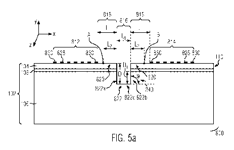
Figures 5a and 5b illustrate a coupled cavity surface acoustic wave filter
structure
-- according to a third embodiment of the invention.
In the third embodiment, like for the first embodiment shown in Figures la and
1 b, the
coupled cavity surface acoustic wave filter structure 800 is realized on a
composite substrate
102 being the same as the substrate 102 of Figures la and lb.
The same reference numbers as in Figure la and lb will be used to refer to the
same
features and will not be explained again in details.
In this embodiment, the thin 5i02 layer 108 provided at the interface 110
between the
piezoelectric layer 104 and the base substrate 106 to improve the attachment
of the
CA 03106887 2021-01-19
WO 2020/021029 2 1
PCT/EP2019/070082
piezoelectric material layer 104 to the base substrate 106 is 500nm thick.
The coupled cavity filter structure 800 comprises two transducer structures
812, 814
and one reflecting structure 816, positioned between the two transducer
structures 812, 814
at a certain distance L of the transducer structures 812, 814 in the direction
of propagation X
as shown in Figure 5a.
Each transducer structure 812, 814 comprises two electrodes 824, 826 (not
shown),
each comprising a plurality of electrode means 828, 830 respectively. The comb
electrodes
are connected to a +VI-V potential in an alternative manner, the electrode 824
at a +V and the
electrode 826 at ¨V, or vice-versa. In a variant, the electrodes 824, 826 can
be comb
electrodes, in particular inter-digitated electrodes.
The transducer structures 812, 814 are defined by the electrode pitch p (not
shown),
corresponding to the edge-to-edge electrode finger distance between two
neighbouring
electrode fingers 828, 830 from opposite comb electrodes 824 and 826.
In this embodiment, the electrode pitch p of the transducer structures 812,
814 is
defined by a number of wavelength nA, A being the operating acoustic
wavelength of said
transducer structures 812, 814.
A metallic ratio a/p of the transducer structure is defined as the ratio of
the width of the
electrode a over p the pitch of the electrode.
In this embodiment of the invention, the reflecting structure 816 is realized
by a groove
822, and is defined by the dimension L1 corresponding to the distance between
the two side
edge walls 822a and 822b of the groove 822 and by its total depth D. The total
depth D of the
groove 822 is defined between the surface of the piezoelectric layer 104 where
the transducer
812, 814 are positioned to the bottom surface 822c of the groove 822. The
depth D of the
groove 822 is of the order of 2, or more, in particular is of the order of la
or more, 2, being the
wavelength of the surface acoustic wave.
Furthermore, the groove 822 is also defined by the etching relief angle 8340,
defining
the position of the edge walls 822a, 822b of the groove in regards to the
horizontal axis X and
the bottom surface of the groove 822c. The relief angle 0 840 can be of the
order of 70 or
more, in particular is of the order of 90 . Figure 5a illustrates a groove 822
with a vertical edge
wall corresponding to a relief angle 8 340 of 90 .
The region located between the reflecting structure 816 and a transducer
structure 812,
814, for example the region 818 with its width defined by the distance L2,
corresponds to an
CA 03106887 2021-01-19
WO 2020/021029 22
PCT/EP2019/070082
acoustic cavity 820. The distance L2 is defined as the distance between one
edge wall 822a,
822b of the groove 822 and a point A, B situated on the surface of the
piezoelectric layer where
the transducers 812, 814 are located. The point A, B is located at the end of
the pitch of the of
the transducer structure 812, 814, on the side where the groove 822 is
located, as shown in
Figure 5a. As the electrodes are centered within the pitch, the end of the
pitch of the tranducer
structure 812, 814 does not correspond to the end of the first electrode 830
of the transducer
structure 812, 814. For example, when the ratio a/p is 50%, the end of the
pitch is located at a
distance equal to 2J8 of the first electrode 830 of the transducer structure
812, 814. Figure 5b
corresponds to figure 5a with the transducer structures 812, 814 comprising
only two
electrodes 828 and 830 in order to show more clearly the regions 818 of the
acoustic cavities
820.
In the coupled cavity surface acoustic wave filter structure 800, two acoustic
cavities
820 are present in the direction of propagation of the acoustic wave, in the
coupled cavity filter
structure shown in Figures 5a and 5b.
In this embodiment of the invention, the reflecting structure 816 is realized
by providing,
e.g. by etching, a groove 822 instead of depositing metallic strips like in
the first and second
embodiments.
The groove 822 is provided in the piezoelectric layer 104 of the composite
substrate
102 and in the SiO2 layer down into the base substrate 106 to a total depth D.
D1 corresponds
to the part of the depth D that is realized in the base substrate 106 only.
In a variant, the groove 822 can be etched only through the piezoelectric
layer 104 and
through the SiO2 layer 108 down to the surface of the base substrate 106 being
the interface
810 between the SiO2 layer 108 and the base substrate 106. Thus, D1 would be
equal to 0.
In a fourth embodiment, based on the third embodiment, the coupled cavity
filter
structure 900 further comprises two Bragg mirrors 832, 834. This embodiment is
shown in
figure 6, where each Bragg mirror 832, 834 is positioned next to a transducer
structure 812,
814 on the other side where the reflecting structure 816 is located, in the
direction of
propagation X of the acoustic wave.
Each Bragg mirror 832, 834 is positioned at a distance s of its respective
transducer
structure 812, 814. Each Bragg mirror 832, 834 comprises one or more metallic
strips 836 and
is defined by the pitch of the metallic strips 836, corresponding to the
distance between the
metallic strips 836 within the Bragg mirror 832, 834. Like for the transducer,
the pitch in the
Bragg mirror 832, 834 is defined by having the metallic strips 840 centered
within the pitch.
CA 03106887 2021-01-19
WO 2020/021029 23
PCT/EP2019/070082
In this variant, the pitch of the Bragg mirror 832, 834 is also equal to a
multiple n of
wavelength 2, so nil.
In this case, on the side where the Bragg mirror 832, 834 is located, the wave
will be
reflected with a phase change, while on the side of the groove, the type of
reflection will depend
on the width and depth of the groove.
In a fifth embodiment, based on the third embodiment, the coupled cavity
filter structure
1000 comprises two additional grooves 932, 934, each additional groove 932,
934 being
positioned next to a transducer structure 812, 814 on the other side where the
reflecting
structure 816 is located, in the direction of propagation of the acoustic
wave. This embodiment
is shown in figure 7.
Each additional groove 932, 834 is positioned at a distance s of its
respective
transducer structure 812, 814. Each additional groove 932, 934 is defined by
its width L3 and
its total depth D3. The total depth D3 of the additional groove 932, 934 is
defined between the
surface of the piezoelectric layer 104 where the transducers 812, 814 are
positioned to the
bottom surface 932c, 934c of the additional groove 932, 934. A depth D2 is
defined as the
depth of the additional groove 932, 934 from the bottom surface 822c of the
groove 822 to the
bottom surface 932c, 934c of the groove 932, 934. Thus, the total depth D3 is
defined as D
plus D2, D being the total depth of the groove 822 of the reflecting structure
816. The depth D3
of the at least one additional groove (932, 934) is of the order of 2, or
more.
In this embodiment of the invention, the reflecting structure 816 and the
additional
grooves 932, 934 are realized by providing, e.g. by etching, grooves instead
of depositing
metallic strips like in the first and second embodiments.
Each additional groove 932, 934 is configured to have a total reflection of
the
propagating wave along the propagation direction.
In a variant, the coupled cavity filter structure can comprise a Bragg mirror
and a groove
each positioned next to a transducer structure 812, 814 on the other side
where the reflecting
structure 816 is located, in the direction of propagation X of the acoustic
wave on one side of
the input transducer and a groove on the side of the output transducer.
The coupled cavity filter device according to one of the third to fifth
embodiment
operates like the coupled cavity filter device according to the first
embodiment, but its structural
features, i.e. the pitch of the transducers and the mirrors, the dimensions of
the cavities are
adapted, so that the conditions are met for the device to show similar
functionality to the first
embodiment.
CA 03106887 2021-01-19
WO 2020/021029 2 4
PCT/EP2019/070082
This is because in the case of a reflection on an edge, the definition of the
reflection
location is geometrically defined. Therefore, whatever the origin of the phase
within the
transducer, the phase construction will occur only for an integer number of
wavelengths. A
Bragg mirror equivalent reflection center is more difficult to define as it
exhibits a phase
variation which mainly depends on the reflection strength. The reflection
function of the Bragg
mirror is defined as the ratio of the reflected versus incident waves defined
at one edge of the
mirror. It is known in the art that the magnitude of the reflection
coefficient on a single electrode
of the grating is conditioning the width of the spectral band corresponding to
the reflection
operation of the grating. However, as the phase variation of the reflection
function between the
beginning and the end of the mirror stop-band is always in the range pi -
2xpi, it appears that
the magnitude of the reflection coefficient also impacts the phase variation
of the reflection
coefficient vs frequency.
Thus, replacing the reflecting structure comprising metallic strips of the
first and second
embodiment by the reflecting structure comprising a groove as in the third,
fourth, fifth and
sixth embodiment results in the condition of having a multiple of 2 for the
coupled cavity filter
device to function.
All the variants of the coupled cavity filter device according to the first
and second
embodiments can also be applied to the coupled cavity filter device according
to the third,
fourth, fifth and sixth embodiment.
Figures 8a to 8h illustrate a coupled cavity surface acoustic wave filter
structure
according to a sixth embodiment of the invention and its variants.
The substrate shown in Figure 8a and 8b is the same as the substrate 102 of
Figures
5a, 5b, 6 and 7. The same reference numbers as in Figure 7 will be used to
refer to the same
features and will not be explained again in details.
In Figure 8a, the coupled cavity filter structure 1100 comprises like the
coupled cavity
filter structure 1000, two transducer structures 812, 814 with two grooves
932, 934 each
positioned next to one transducer structure. The difference with the coupled
cavity filter 900 is
that a plurality of reflecting structures, namely two reflecting structures
1006 and 1016 are
present in between the transducer structures 812, 814. Each reflecting
structure 1006, 1016
of the plurality of reflecting structure corresponds to a groove 1022 and are
defined by the
width L1 and the total depth D of the groove 1022.
These reflecting structures 1006, 1016 are separated from each other by a gap
gin the
direction of propagation X. The region 1008 located in between the two
adjacent reflecting
structures 1006, 1016, with its width defined by the gap g, corresponds to an
acoustic cavity
CA 03106887 2021-01-19
WO 2020/021029 25
PCT/EP2019/070082
1010. The acoustic cavity 1010 can be considered as a central cavity, while
the cavities 1020
can be called the side cavities.
Like for the coupled cavity filter structure 800 and 900, the regions 1018
located
between a reflecting structure 1006, 1016 and an adjacent transducer structure
812, 814
corresponds also to an acoustic cavity 1020, with a width defined by the
distance L2 between
the edge of the reflective structure 1006, 1016 and the point A, B located on
the piezoelectric
layer 104 surface.
The region 1008 actually comprises the piezoelectric layer 104 and the SiO2
layer 108
on top of the base substrate 106.
Thus, in the coupled cavity surface acoustic wave filter structure 1100, three
cavities
are present in the direction of propagation of the acoustic wave, being
separated by a reflecting
structure, or said otherwise, a cavity is surrounded by two reflecting
structures in between the
transducer.
In another variant of the sixth embodiment, the coupled cavity surface
acoustic wave
filter structure 1200, as shown in Figure 8b, has a region 1008 between the
grooves 1006 and
1016 which is devoid the piezoelectric layer 104 and devoid the SiO2 layer
108. In the region
1008 only the base substrate 106 is present. According to a further variant,
the surface of the
base substrate could also be etched so that the thickness of the base
substrate in the region
1008 would be smaller than in the regions 1018.
For all the figures 8c to 8h, illustrating further variants with sub-cavities,
the coupled
cavity filter structure 1300 to 1800 are shown in a 2D plan view from the top.
In the coupled cavity filter structure 1300 as shown in Figure 6c, the two
reflecting
structures 1206, 1216 of the plurality of reflecting structures are separated
from each other by
a gap w but in the direction of propagation Z. The region 1208, like the
region 1008 of Figure
8a can be or not etched. In this case, the acoustic cavities 1020 are split
into two sub-cavities
1020a, 1020b.
In the coupled cavity filter structure 1400, like in the cavity filter device
1100, a plurality
of reflective structures 1316 are separated from each other by a gap g in the
direction of
propagation X, and like for the cavity filter device 1200, the plurality of
reflective structures
1316 are also separated from each other by a gap w but in the direction of
propagation Z. The
regions 1308 in between the plurality of reflective structures, like the
region 1008 of Figure 8a
and the regions 1210 of Figure 8c can be or not etched.
CA 03106887 2021-01-19
WO 2020/021029 2 6
PCT/EP2019/070082
In this variant, the acoustic cavities 1310, 1320 are split into a plurality
of sub-cavities
1310a, 1310b, 1320a, 1320b, like the device 600 according to the second
embodiment of the
invention.
In the coupled cavity filter structure 1500, as shown in Figure 8e, the
plurality of
reflective structures 1506, 1516 are symmetrically separated by a central
region 1510 with a
width wi in the direction Z, along the whole distance between the two
transducer structures
812, 814, where no reflective structures 1506, 1516 are present. Furthermore,
instead of being
elongated etched grooves in the Z direction as in the previous variants, the
grooves 1522 are
now in a square form. For clarity purposes, only one reflecting structure
1506, 1516 and one
groove 1522 are noted on the figure 8e.
In the coupled cavity filter structure 1600, shown in Figure 8f, the dimension
of the
region 1610 without reflective structures 1506, 1516 between the transducer
structures 812,
814 is different than region 1510 of the figure 8e. The region 1610 is
actually thinner, with three
reflecting structures being removed in a row in the Z direction. The region
1610 could be
assimilated to a break in symmetry of the plurality of reflective structures.
For clarity purposes,
only one reflecting structure 1506, 1516 and one groove 1522 are noted on the
figure 8f.
In another variant, the device 1700 shown in Figure 8g corresponds to the
device 1500
of Figure 8e with the two additional grooves 1532, 1534 comprising a plurality
of reflecting
structures 1506, 1516 and thus a plurality of grooves 1522.
In a variant of the invention, the coupled cavity filter structure 1800 can
comprise three
transducer structures or even more. In Figure 8h is shown the variant where
three transducers
structures 1210, 1212, 1214 are present in the coupled cavity filter structure
1200.
Two of the transducer structures 1210, 1214 are positioned, like in the
structure of
Figure 2c, on the outside of the reflecting structures 1706, 1716 while the
third transducer
structure 1212 is positioned in the middle of the reflecting structures 1706,
1716, so that on
each side of the third transducer structure 1212, one reflecting structure
1706, 1716, thus, a
groove 1722, is present. The transducer structure 1212 is also separated from
the two adjacent
reflecting structures 1706, 1716 by a distance L, corresponding to the same
distance between
the transducer structure 1210, 1214 and their respective neighbouring
reflecting structure,
here 1706 for the transducer structure 1210 and 1716 for the transducer
structure 1214. Such
a cavity filter structure 1800 is symmetrical and results in a stronger
confinement of energy in
the cavities 1720 compare to the cavity filter structure 1300 as shown in
Figure 8c, with only
two transducer structures 812, 814. Furthermore, here, the reflecting
structures 1706, 1716
CA 03106887 2021-01-19
WO 2020/021029 2 7
PCT/EP2019/070082
are also separated from each other by a distance wi, like in the device 1300
shown in figure
8c.
In a variant of the invention, the third transducer 1210 is not positioned in
the middle of
the coupled cavity filter structure so that the coupled cavity filter
structure is not symmetrical.
Figure 9 shows the device according to the third embodiment of the invention
used for
the simulation.
For this simulation, the device used corresponds to the device 1000 as shown
in Figure
7, but here the transducer structures 812 and 814 comprises only two
electrodes fingers 828,
830 each.
Furthermore, the following parameters for the structure were used. A composite
substrate with a SiO2 layer of 200nm in between a LiTa03 (YX/)/42
piezoelectric layer of
500nm and a semi-infinite (100) Silicon substrate was used for the simulation.
The electrode
pitch of the transducer p is equal to 800nm yielding a wavelength A equal to
1.6pm for a
frequency operation near 2.5GHz. The metallization ratio a/p is equal to 0.5
which means an
electrode width of a equal to 400 nm. The electrode fingers are of Al-Cu with
a thickness set
to 100 nm.
Figures 10a and 10b show the simulated characteristics of the coupled cavity
surface
acoustic wave filter structure as shown in Figure 9, according to an example
of the third
embodiment of the invention.
In this practical example, the simulation was conducted with a mesh structure
(not
shown) with a pitch p equal to 2pm, a depth D1 equal to the pitch p, a depth
D2 equal to 6xp,
a width of the groove L1 equal to 6.4pm and a width L2 equal to 2xp. A
composite substrate
with a 600nm thick LiTa03, a 500nm thick 5i02 on a (100) Si base substrate was
used.
Figure 10a shows a graph of the admittance, real part on the left Y axis and
imaginary
part on the right Axis, as a function of frequency in GHz on the X axis.
Figure 10a shows two
peaks around 61800GHz and 62000GHz, the peak at around 61750GHz showing a
strong
admittance compared to the other peak around 62000GHz.
Figure 10b shows a graph of the trans-admittance, real part on the left Y axis
and
imaginary part on the right Axis, as a function of frequency in GHz on the X
axis. Figure 10b
shows the same two peaks around 61800GHz and 62000GHz, but this time with a
more
balanced contribution, the two peaks being equivalent in amplitude.
CA 03106887 2021-01-19
WO 2020/021029 2 8
PCT/EP2019/070082
The graphs illustrate the two coupled modes, with two balanced contributions
allowing
for an effective definition of a filter bandpass, whatever the actual
amplitude level.
Figures lla to lid show the calculation of admittance of the filter elementary
structure
for various dimensions of the reflecting structure according to the invention.
A composite substrate with a SiO2 layer of 500nm in between a LiTa03 (YX/)/42
piezoelectric layer of 600nm and a semi-infinite (100) Silicon substrate was
used for the
simulation.
Figures 11 a to lib show a graph of the admittance, real part on the left Y
axis and
imaginary part on the right Axis, as a function of frequency in GHz on the X
axis, for varying
depth D1 of the groove. The frequency range shown is between 61000 and
63000GHz. All
graphs show the same two peaks around 61800GHz and 62500GHz as in Figure 10b,
which
could be considered as a double peak formation, with the first peak around
61800GHz with
higher admittance value than the second peak around 63000GHz. In Figure 10d,
the double
peak actually has a thinner bandwidth than in Figure 11a, llb or 10c.
In Figures 11 a to 11 c, D1 varies between 1 ,rn and 0.4m, while in Figure
11d, D1 varies
between 1 ,rn and 2[trn.
In Figure lla to 11d, the same behaviour of the peaks can be seen. As D1
decreases
from 1 ,rn to 0.4m, the double peak formation moves towards higher frequency,
while the first
peak decreases in admittance and the second peak increases in admittance. In
Figure lib,
11c and 11d, the second peak increases in admittance so that it actually
reaches higher values
than the first peak, while in Figure 11a, both peaks are equivalent for D1
equal to 0.4m.
Figures 12a and 12b illustrate an example of a SAW ladder filter device
according to
the state of the art in Figurel 2a and according to the invention in Figure
12b.
In Figure 12a, four transducer structures 1612, 1614, 1616 and 1618 are each
sandwiched between two reflecting structures 1632 and 1634. The inter-
digitated electrodes
of the transducers 1612, 1614, 1616, 1618 are connected to each other by
metallic lines 1640.
As can be seen, such design is bulky as the transducers and their metallic
connections require
a lot of space. The transducers cannot be aligned on a single line, either
vertical or horizontal
as they need to be shifted one to another to allow the connections between the
transducers.
Figure 12b shows a SAW ladder filter device 2000 where two cavity coupled
filter
device 1000 according to the invention are positioned next to each other on a
single line. Each
cavity coupled filter device 1000 comprises two transducer structures 1712,
1714 and 1716,
CA 03106887 2021-01-19
WO 2020/021029 2 9
PCT/EP2019/070082
1718 respectively, with their respective reflecting structures 1732, 1734 and
1716. The
reflecting structure 1716 is located in between two transducer structures, for
example 1716 in
between 1712 and 1714, and the reflecting structures 1732 and 1734 are
positioned each on
one side of a transducer structure, opposite to the side where the reflecting
structure 1716 is
positioned. In Figure 12b, the reflecting structures 1716, 1734 and 1732 are
represented as
grooves, as in Figure 8. Like in Figure 12a, the electrodes of the transducers
are connected to
each other by metallic lines 1740.
The SAW ladder filter device 2000 is shown in Figure 12b with two cavity
coupled filter
device 1000, but any variants of the cavity coupled filter device 1000
according to the invention
can be used for the SAW ladder filter device.
The SAW ladder filter device 2000 according to the invention is compacter and
does
not require as much space as the SAW ladder filter device shown on Figure 12a.
A number of embodiments of the invention have been described. Nevertheless, it
is
understood that various modifications and enhancements may be made without
departing the
following claims.