Note: Descriptions are shown in the official language in which they were submitted.
CA 03108481 2021-02-02
WO 2020/027854
PCT/US2018/045203
DETERMINING AN INPUT VOLTAGE TO A GALVANIC ISOLATION POINT
TECHNICAL FIELD
The embodiments described below relate to electronics including a galvanic
isolation point and, more particularly, to determining an input voltage to a
galvanic
isolation point.
BACKGROUND
In industrial control products communication must occur in potentially
hazardous
and electrically noisy environments while utilizing limited computation and/or
power
resources. Because of the potentially hazardous and/or electrically noisy
environments
in which industrial control products are employed, many products include
electrical
isolation between input/output (I/O) channels, sensor connection, and/or
processing
functions. In non-hazardous installations, this isolation is provided to
eliminate possible
ground loop and noise sources since I/O channels may be directed to different
systems.
In hazardous area installations, the isolation may be necessary to meet
approval
standards.
A transformer may be used to electrically isolate an input and an output
voltage.
The transformer may be part of a DC/DC converter, such as a flyback converter.
FIG. 1
shows an exemplary flyback converter 10. As shown in FIG. 1, the flyback
converter 10
includes an input voltage source 11 and an isolation transformer 12. The
isolation
transformer 12 is coupled to the input voltage source 11 and is configured to
receive an
input voltage Vin provided by the input voltage source 11. The isolation
transformer 12
is also coupled to a rectifier circuit 13. The rectifier circuit 13 is
comprised of a rectifier
diode D1 and an output capacitor Cout. A switch 15 is coupled to the isolation
transformer 12 and is configured to allow a current to flow from the input
voltage source
11 through the isolation transformer 12.
The isolation transformer 12 serves as a galvanic isolation point. That is, an
output voltage provided by the flyback converter 10 may not include noise,
transients,
high voltage, or the like, that may be induced by current flow between input
and output
sections that would be possible in the absence of the gavanic isolation point.
The
flyback converter 10 may be included in an electronics (e.g., an electronic
device) that
1
CA 03108481 2021-02-02
WO 2020/027854
PCT/US2018/045203
needs to determine the input voltage Vin to ensure that the input voltage Vin
is within
specification. For example, in a loop powered device, power may be consumed on
the
secondary or galvanically isolated side of the device's electronics, including
measurement transducer(s) and associated signal processing circuitry. The
power must
be provided by the loop coupled to the input or primary side of the device,
which may
not be sufficient for the measurement transducer and associated signal
processing
circuitry.
The electronics may also need to determine the input voltage Vin using
circuits
on the secondary or galvanically isolated side of the electronics. However,
adding an
additional galvanic isolation point (e.g., an additional transformer) to
transmit a
measured value of the input voltage Vin requires additional board space. In
addition,
significant costs may be incurred in modifying existing electronic designs to
incorporate
the additional galvanic isolation point that may be avoided if the existing
galvanic
isolation point can be utilized. Therefore, there is a need to determine the
input voltage
to the galvanic isolation point without requiring the additional galvanic
isolation point.
SUMMARY
An electronics configured to determine an input voltage to a galvanic
isolation
point of the electronics is provided. According to an embodiment, the
electronics
comprises an isolation transformer configured to conduct a primary current
provided by
an input voltage source, and provide a secondary voltage, the secondary
voltage being
proportional to a primary voltage induced by the primary current. The
electronics also
comprises a peak detection circuit coupled to the isolation transformer, the
peak
detection circuit being configured to receive the secondary voltage and, based
on the
secondary voltage, provide a signal that is proportional to the primary
voltage.
A method for determining an input voltage to a galvanic isolation point is
provided. According to an embodiment, the method comprises conducting a
primary
current provided by an input voltage source through an isolation transformer,
providing
a secondary voltage with the isolation transformer, the secondary voltage
being
proportional to a primary voltage induced by the primary current, receiving
the
secondary voltage with a peak detection circuit, and based on the secondary
voltage,
2
CA 03108481 2021-02-02
WO 2020/027854
PCT/US2018/045203
providing with the peak detection circuit a signal that is proportional to the
primary
voltage.
ASPECTS
According to an aspect, an electronics (100) configured to determine an input
voltage to a galvanic isolation point of the electronics (100) comprises an
isolation
transformer (120) configured to conduct a primary current (Ip) provided by an
input
voltage source (110), and provide a secondary voltage (Vs), the secondary
voltage (Vs)
being proportional to a primary voltage (Vp) induced by the primary current
(Ip). The
electronics (100) also comprises a peak detection circuit (130) coupled to the
isolation
transformer (120), the peak detection circuit (130) being configured to
receive the
secondary voltage (Vs) and, based on the secondary voltage (Vs), provide a
signal that
is proportional to the primary voltage (Vp).
Preferably, the electronics (100) further comprises a rectifier circuit (140)
coupled to the isolation transformer (120), the rectifier circuit (140) being
configured to
receive the secondary voltage (Vs) and provide to a load (L) a capacitor
voltage when
the secondary voltage (Vs) is at a negative value, and the secondary voltage
(Vs) when
the secondary voltage (Vs) is a positive value.
Preferably, the rectifier circuit (140) is comprised of a rectifier diode (D1)
in a
series electrical connection with the isolation transformer (120) and
configured to
provide the secondary voltage (Vs) to the load (L) when the secondary voltage
(Vs) is
the positive value by conducting a secondary current (Is) provided by the
isolation
transformer (120). The rectifier circuit (140) is also comprised of an output
capacitor
(Cout) in a parallel electrical connection with the isolation transformer
(120), the output
capacitor (Cout) being configured to receive the secondary voltage (Vs) when
the
rectifier diode (D1) is conducting the secondary current (Is).
Preferably, the rectifier diode (D1) is further configured to prevent a
current flow
when the secondary voltage (Vs) is at the negative value.
Preferably, the peak detection circuit (130) is further configured to hold a
first
voltage value of the secondary voltage (Vs) when the secondary voltage (Vs) is
at a
second voltage value that is greater than the first voltage value.
3
CA 03108481 2021-02-02
WO 2020/027854
PCT/US2018/045203
Preferably, the peak detection circuit (130) is comprised of a peak detect
diode
(D2) in a series electrical connection with a peak hold capacitor (C1), the
peak detection
circuit (130) being in a parallel electrical connection with the isolation
transformer
(120).
Preferably, the peak hold capacitor (Cl) is configured to hold the first
voltage
value of the secondary voltage (Vs) when the secondary voltage (Vs) is at the
second
voltage value that is greater than the first voltage value, and the peak
detect diode (D2)
is configured to conduct a current when the second voltage value of the
secondary
voltage (Vs) is less than the first voltage value.
Preferably, the secondary voltage (Vs) is proportional to the primary voltage
(Vp) by a secondary-to-primary turns ratio (Ns/Np) of the isolation
transformer (120).
A method for determining an input voltage to a galvanic isolation point
comprises conducting a primary current provided by an input voltage source
through an
isolation transformer, providing a secondary voltage with the isolation
transformer, the
secondary voltage being proportional to a primary voltage induced by the
primary
current, receiving the secondary voltage with a peak detection circuit, and
based on the
secondary voltage, providing with the peak detection circuit a signal that is
proportional
to the primary voltage.
Preferably, the method further comprises receiving with a rectifier circuit
the
secondary voltage and providing to a load with a rectifier circuit a capacitor
voltage
when the secondary voltage is a negative value and the secondary voltage when
the
secondary voltage is a positive value.
Preferably, providing to the load with the rectifier circuit the capacitor
voltage
when the secondary voltage is a positive value comprises providing with a
rectifier
diode in the rectifier circuit in a series electrical connection with the
isolation
transformer by conducting a secondary current provided by the isolation
transformer,
and receiving with an output capacitor in a parallel electrical connection
with the
isolation transformer the secondary voltage when the rectifier diode is
conducting the
secondary current.
Preferably, the method further comprises preventing current flow with the
rectifier diode when the secondary voltage is at the negative value.
4
CA 03108481 2021-02-02
WO 2020/027854
PCT/US2018/045203
Preferably, the method further comprises holding with the peak detection
circuit
a first voltage value of the secondary voltage when the secondary voltage is
at a second
voltage value that is greater than the first voltage value.
Preferably, the method further comprises providing a peak detect diode and a
peak hold capacitor, and connecting the peak detect diode and the peak hold
capacitor in
series to comprise the peak detection circuit.
Preferably, the method further comprises holding with the peak hold capacitor
the first voltage value when the secondary voltage is at the second voltage
value greater
than the first voltage value and configuring the peak detect diode to conduct
current
when the second voltage value is less than the first voltage value.
Preferably, the secondary voltage is proportional to the primary voltage by a
secondary-to-primary turns ratio of the isolation transformer.
BRIEF DESCRIPTION OF THE DRAWINGS
The same reference number represents the same element on all drawings. It
should be understood that the drawings are not necessarily to scale.
FIG. 1 shows an exemplary flyback converter 10.
FIG. 2 shows an electronics 100 configured to determine an input voltage to a
galvanic isolation point.
FIG. 3 shows a graph 300 illustrating various electrical values and states in
an
electronics configured to determine an input voltage to a galvanic isolation
point of the
electronics.
FIG. 4 shows a method 400 for determining an input voltage to a galvanic
isolation point.
DETAILED DESCRIPTION
FIGS. 2 ¨ 4 and the following description depict specific examples to teach
those
skilled in the art how to make and use the best mode of embodiments of
electronics and
methods that can determine an input to a galvanic isolation point. For the
purpose of
teaching inventive principles, some conventional aspects have been simplified
or
omitted. Those skilled in the art will appreciate variations from these
examples that fall
within the scope of the present description. Those skilled in the art will
appreciate that
5
CA 03108481 2021-02-02
WO 2020/027854
PCT/US2018/045203
the features described below can be combined in various ways to form
electronics and
methods that can determine an input to the galvanic isolation point. As a
result, the
embodiments described below are not limited to the specific examples described
below,
but only by the claims and their equivalents.
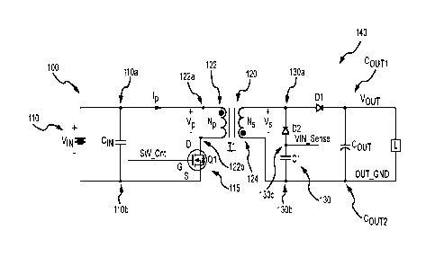
FIG. 2 shows an electronics 100 including a galvanic isolation point. As shown
in FIG. 2, the electronics 100 includes an input voltage source 110 that is
coupled to an
isolation transformer 120. The isolation transformer 120 is the galvanic
isolation point
of the electronics 100. A peak detection circuit 130 is coupled to the
isolation
transformer 120. A switch 115 is coupled to the isolation transformer 120 and
is
configured to selectively conduct a current based on a switch control signal
SW_Cntl.
Also shown is a rectifier circuit 140 that is coupled to the isolation
transformer 120. The
topology of the electronics 100 is a flyback converter, although the peak
detection
circuit 130 and rectifier circuit 140 may be employed in other topologies,
such as a
flybuck converter.
The input voltage source 110 provides an input voltage Vin. The input voltage
source 110 may provide a constant voltage, such as a direct current (DC)
voltage, to the
isolation transformer 120. The input voltage source 110 may be in a non-
isolated side of
a galvanic isolation point. As a result, the input voltage Vin may include
noise,
transients, high voltages, or the like. The input voltage source 110 may be
any suitable
source, such as a two-wire bus, an external power supply, a battery or power
supply in
the electronics 100, etc. The input voltage source 110 has a first input
voltage source
terminal 110a and a second input voltage source terminal 110b.
The switch 115 is shown as being comprised of a metal-oxide semiconductor
field effect transistor (MOSFET), although any suitable switch may be
employed. As
shown, the MOSFET includes a gate G, drain D, and source S terminals. The
switch 115
is connected to the second input voltage source terminal 110b. The switch 115
is
configured to receive the switch-control signal SW_Cntl. Where the switch 115
is
comprised of the MOSFET shown in FIG. 2, the source S is electrically
connected to the
second input voltage source terminal 110b and the gate G receives the switch-
control
signal.
The isolation transformer 120 includes a primary coil 122 and a secondary coil
124. The isolation transformer 120 may be any suitable configuration and is
not
6
CA 03108481 2021-02-02
WO 2020/027854
PCT/US2018/045203
necessarily limited to transformers. For example, the isolation transformer
120 may be
comprised of coupled inductors. As shown, the primary coil 122 is comprised of
an
inductor that has a first primary terminal 122a and a second primary terminal
122b. The
first primary terminal 122a is electrically connected to the first input
voltage source
terminal 110a of the input voltage source 110. The second primary terminal
122b is
electrically connected to the second input voltage source terminal 110b and
the switch
115.
As shown, the primary coil 122 is denoted as having a primary voltage Vp and
the secondary coil 124 is denoted as having a secondary voltage Vs. The
primary coil
122 is shown as having Np number of turns and the secondary coil 124 is shown
as
having Ns number of turns. Accordingly, the primary voltage Vp may be
proportional to
the secondary voltage Vs by a secondary-to-primary turns ratio (Ns/Np) of the
isolation
transformer 120. However, any suitable relationship may be employed.
The isolation transformer 120 may conduct a primary current Ip that is
provided
by the input voltage source 110. That is, the input voltage source 110 may
provide the
input voltage Vin to the isolation transformer 120 and the switch 115 may
selectively
close a circuit between the first input voltage source terminal 110a and the
second input
voltage source terminal 110b. As a result, the primary voltage Vp is equal to
the input
voltage Vin, thereby causing the isolation transformer 120 to conduct the
primary
current Ip. Due to inductive coupling, the primary current Ip may induce the
secondary
voltage Vs on the secondary coil 124. The secondary voltage Vs may be provided
to the
peak detection circuit 130.
The peak detection circuit 130 is configured to receive the secondary voltage
Vs.
As shown in FIG. 2, the peak detection circuit 130 includes a first voltage
determination
terminal 130a and a second voltage determination terminal 130b. The first
voltage
determination terminal 130a is electrically connected to a first secondary
terminal and
the second voltage determination terminal 130b is electrically connected to a
second
secondary terminal. Accordingly, the secondary voltage Vs is applied to the
first and
second voltage determination terminals 130a, 130b of the peak detection
circuit 130.
The peak detection circuit 130 may also be configured to provide a signal
Vin_sense via a signal terminal 130c. The signal may be proportional to the
primary
voltage Vp. As shown in FIG. 2, for example, the signal Vin_sense is
proportional to the
7
CA 03108481 2021-02-02
WO 2020/027854
PCT/US2018/045203
primary voltage Vp due to the peak detection circuit 130 holding the secondary
voltage
Vs. For example, the signal Vin_sense provided by the peak detection circuit
130 may
be a voltage value of the secondary voltage Vs. The voltage value of the
secondary
voltage Vs may be proportional to the primary voltage Vp by the secondary-to-
primary
turns ratio of the isolation transformer 120.
As shown in FIG. 2, the peak detection circuit 130 is comprised of a peak
detect
diode D2 in series with the peak hold capacitor Cl. The peak detect diode D2
is
electrically connected to the peak hold capacitor Cl at the signal terminal
130c. The
peak detect diode D2 is arranged so as to allow a current to conduct from the
peak hold
capacitor Cl to the first voltage determination terminal 130a. The peak detect
diode D2
is also arranged to prevent current from conducting from the first voltage
determination
terminal 130a to the peak hold capacitor Cl.
As a result, when the secondary voltage Vs is negative, where the first
voltage
determination terminal 130a is a negative terminal and the second voltage
determination
terminal 130b is a positive terminal, the peak detect diode D2 can allow
current to flow
from the peak hold capacitor Cl to the first voltage determination terminal
130a. This
may allow the peak hold capacitor Cl to be charged to a voltage value of the
secondary
voltage Vs.
When the secondary voltage Vs is positive, where the first voltage
determination
terminal 130a is a positive terminal and the second voltage determination
terminal 130b
is a negative terminal, then the peak detect diode D2 prevents current flow
from the first
voltage determination terminal 130a to the peak hold capacitor Cl. This allows
the peak
hold capacitor Cl to hold the voltage value of the secondary voltage Vs. That
is, the
peak hold capacitor Cl is not discharged. Accordingly, the signal Vin_sense is
still
provided.
As discussed above, the topology of the electronics 100 may be a flyback
converter, although the peak detection circuit 130 and/or rectifier circuit
140 may be
employed in other topologies, such as a flybuck converter. In a flybuck
converter,
output voltage of the "buck" winding may need to be subtracted off a signal
provided by
the peak detect circuit to derive the input voltage. The peak detection
circuit 130 may be
used in any topology where the input voltage has an amplitude that is
discernable at the
output side winding of an isolation transformer.
8
CA 03108481 2021-02-02
WO 2020/027854
PCT/US2018/045203
The rectifier circuit 140 is configured to provide an output voltage Vout
that, for
example, may be a substantially constant DC value. As shown in FIG. 2, the
rectifier
circuit 140 may receive the secondary voltage Vs from the isolation
transformer 120 and
provide the output voltage Vout. As is discussed above and explained in more
detail in
the following with reference to FIG. 3, the secondary voltage Vs may have a
negative
voltage value or a positive voltage value. When the secondary voltage Vs has a
positive
voltage value, the rectifier circuit 140 can provide the secondary voltage Vs
as the
output voltage Vout. When the secondary voltage Vs has a negative voltage
value, then
the rectifier circuit 140 may not receive the secondary voltage Vs but may
nevertheless
provide the output voltage Vout. The output voltage Vout is provided to a load
L.
As shown in FIG. 2, the rectifier circuit 140 is comprised of a rectifier
diode D1
and an output capacitor Cout. The rectifier diode D1 is also electrically
connected to an
output capacitor Cout. The rectifier diode D1 is arranged to conduct current
from the
first voltage determination terminal 130a to the output capacitor Cout. The
output
capacitor Cout has a first output terminal Coutl and a second output terminal
Cout2.
The first output terminal Coutl is electrically connected to the rectifier
diode Dl. The
second output terminal Cout2 is electrically connected to the second voltage
determination terminal 130b. A voltage difference between the first output
terminal
Coutl and the second output terminal Cout2 is shown as being the output
voltage Vout.
The rectifier diode D1 may prevent a current flow from the first output
terminal
Coutl to the first voltage determination terminal 130a. Accordingly, if the
secondary
voltage Vs has a voltage value that is less than a voltage value at the first
output
terminal Coutl, then the rectifier diode D1 may prevent the current flow from
the output
capacitor Cout to the isolation transformer 120. The rectifier diode D1 may
also allow a
current flow from the first voltage determination terminal 130a to the first
output
terminal Coutl to, for example, charge the output capacitor Cout. That is, if
the
secondary voltage Vs has a voltage value that is greater than a voltage value
at the first
output terminal Coutl, then the rectifier diode D1 may allow the current flow
to the first
output terminal Coutl.
As a result, the output voltage Vout may be substantially constant at a
voltage
value that is approximately equal to the voltage value of the secondary
voltage Vs that
causes the rectifier diode D1 to allow the current flow to the first output
terminal Coutl.
9
CA 03108481 2021-02-02
WO 2020/027854
PCT/US2018/045203
The output voltage Vout remains substantially constant even though the peak
detection
circuit 130 is providing the signal at the signal terminal 130c that is
proportional to the
input voltage Vin. That is, the various electrical values and states in the
electronics
allow the peak detection circuit 130 to determine the input voltage Vin while
also being
isolated from the input voltage source 110. The electrical values and states
in an
electronics are discussed in more detail in the following with reference to
FIG. 3.
FIG. 3 shows a graph 300 illustrating various electrical values and states in
an
electronics configured to determine an input voltage to a galvanic isolation
point of the
electronics. As shown in FIG. 3, the graph 300 includes a first through fifth
time axes
310a-310e and a state/value axis 320. The first through fifth time axes 310a-
310e are in
units of seconds, although any suitable unit may be employed. The state/value
axis 320
is in units of volts, amps, or bit-state depending on which of the first
through fifth time
axes 310a-310e is being referenced. As shown in FIG. 3, the graph 300 includes
a
switch-control plot 330a, a primary voltage Vp plot 330b, a secondary voltage
Vs plot
330c, a primary current Ip plot 330d, and a secondary current Is plot 330e.
The switch-control plot 330a is shown as being comprised of an "on" or an
"off'
state. The switch-control plot 330a may represent the switch-control signal
that is
provided to the switch 115 described with reference to FIG. 2. As can be
appreciated,
the switch-control plot 330a alternates between the "on" and the "off' state
in a periodic
manner. The frequency of the switch-control plot 330a may be, for example,
100kHz to
200kHz, although any suitable frequency or frequencies may be employed. Also,
any
suitable periods or other ways of controlling the switch 115 or the primary
current Ip
shown in FIG. 2 may be employed.
The primary voltage Vp plot 330b is shown as being comprised of a first
voltage
value 330ba and a second voltage value 330bb. The first voltage value 330ba is
shown
as being equal to an input voltage Vin, which may be provided by the input
voltage
source 110 shown in FIG. 2. As can be appreciated, alternative first voltage
values may
be employed, such as, for example, where there are additional components
between an
input voltage source and an isolation transformer.
The secondary voltage Vs plot 330c is shown as being comprised of a first
voltage value 330ca and a second voltage value 330cb. The first voltage value
330ca is
shown as being equal to -Vin(Ns/Np). That is, the first voltage value 330ca is
CA 03108481 2021-02-02
WO 2020/027854
PCT/US2018/045203
proportional to the input voltage Vin by -Ns/Np, although any suitable
relationship may
be employed, such as turns ratios associated with multiple winding
transformers, center
tap transformers, ratios associated with coupled inductors, etc. The second
voltage value
330cb is shown as being equal to an output voltage Vout. That is, the second
voltage
value 330cb is the output voltage Vout due to, using FIG. 2 as an example, the
rectifier
diode D1 allowing current flow to the output capacitor Cout.
The primary current Ip plot 330d is shown as being comprised of a first
current
value 330da and second current value 330db. The first current value 330da is
shown as
having a positive and increasing value. The second current value 330db is
shown as
being zero. The first current value 330da may be positive due to, for example,
the switch
115 being closed, thereby closing the circuit to the input voltage source 110.
This allows
the primary current Ip to flow through the isolation transformer 120. The
second current
value 330db may be zero because the switch 115 is open, thereby preventing
current
flow from the input voltage source 110.
The secondary current Is plot 330e is shown as being comprised of a first
current
value 330ea and a second current value 330eb. The first current value 330ea is
shown as
being zero. The second current value 330eb is shown as having a positive and
decreasing value. The first current value 330ea may be zero due to the
rectifier diode D1
preventing a current flow from the first output terminal Coutl to the
isolation
transformer 120. The second current value 330eb may be positive due to the
rectifier
diode D1 allowing current flow from the isolation transformer 120 to the first
output
terminal Coutl.
Turning to the peak detection circuit 130, the peak detect diode D2 allows a
current flow from the peak hold capacitor Cl when the secondary voltage Vs is
at a
voltage value less than a voltage value at the signal terminal 130c. That is,
when the
peak detect diode D2 is forward biased, current may flow to the first voltage
determination terminal 130a. As a result, the voltage value at the signal
terminal 130c
may be equal to the voltage value of the secondary voltage Vs.
When the secondary voltage Vs has a value that is greater than a voltage value
at
the signal terminal 130c, then the peak detect diode D2 may prevent a current
flow from
the first voltage determination terminal 130a to the signal terminal 130c.
That is, when
the peak detect diode D2 is reversed biased, current flow may be prevented
thereby
11
CA 03108481 2021-02-02
WO 2020/027854
PCT/US2018/045203
preventing the peak hold capacitor Cl from being discharged. The peak hold
capacitor
Cl may therefore hold a voltage value, such as the voltage value of the
secondary
voltage Vs that may charge the peak hold capacitor Cl when the peak detect
diode D2 is
forward biased.
Accordingly, when considering the secondary voltage Vs plot 330c, it can be
appreciated that the peak hold capacitor Cl may have a voltage value that is
equal to a
voltage value of ¨Vin(Ns/Np) when the peak hold diode D2 is forward biased.
That is,
when the switch-control plot 330a is "on" where the primary voltage Vp is
equal to Vin,
a voltage value of the signal terminal 130c may be equal to Vs, which is equal
to ¨
Vin(Ns/Np). It can also be appreciated that the peak hold capacitor Cl will
maintain the
voltage value of ¨Vin(Ns/Np) when the peak hold diode D2 is reverse-biased.
Additionally, there may be a load resistance across the peak hold capacitor Cl
(analagous to the load L across output capacitor Cout) which provides a path
for
discharge of the peak hold capacitor Cl at a relatively slow rate, such that
the peak hold
capacitor Cl may not indefinitely hold the largest negative voltage it has
ever been
exposed to.
As can also be appreciated, as the input voltage Vin decreases over time, the
magnitude of the voltage value of a voltage of the peak hold capacitor Cl may
correspondingly decrease. By way of example, the peak hold capacitor Cl may be
.. charged to a first voltage value of ¨Vinl(Ns/Np) during a first "on" state.
If the voltage
value of the input voltage Vin is decreasing over time, then the secondary
voltage Vs
may be at a second voltage value of ¨Vin2(Ns/Np) that is more positive or less
negative
than the first voltage value of ¨Vin 1 (Ns/Np). Accordingly, the voltage value
of the
signal terminal 130c may be at the second voltage value of ¨Vin2(Ns/Np).
Therefore, the signal provided by the signal terminal 130c may be proportional
with the input voltage Vin over time. This allows, for example, the
electronics 100 to
determine the input voltage Vin over time even though the signal terminal 130c
is
isolated from the input voltage source 110. Additionally, the signal is
provided using a
single galvanic point, rather than a separate galvanic point. This reduces the
board space
requirement over the prior art. As can be appreciated, an electronics, such as
the
electronics 100 described in the foregoing, may execute a method to provide
the signal.
An exemplary method is described in the following with reference to FIG. 4.
12
CA 03108481 2021-02-02
WO 2020/027854
PCT/US2018/045203
FIG. 4 shows a method 400 for determining an input voltage to a galvanic
isolation point. As shown in FIG. 4, the method 400 conducts a primary current
provided by an input voltage source through an isolation transformer in step
410. In step
420, the method 400 provides a secondary voltage with the isolation
transformer. The
secondary voltage may be proportional to a primary voltage induced by the
primary
current. In step 430, the method 400 receives the secondary voltage with a
peak
detection circuit. In step 440, the method 400, based on the secondary
voltage, provides
with the peak detection circuit a signal that is proportional to the primary
voltage.
The method 400 may further comprise receiving with a rectifier circuit the
secondary voltage and providing an output voltage or the secondary voltage to
a load
with a rectifier circuit. The output voltage may be provided when the
secondary voltage
is a negative value and the secondary voltage may be provided when the
secondary
voltage is a positive value. Providing to the load with the rectifier circuit
the capacitor
voltage when the secondary voltage is the positive value may comprise
providing with a
rectifier diode in the rectifier circuit in a series electrical connection
with the isolation
transformer by conducting a secondary current provided by the isolation
transformer,
and receiving with an output capacitor in a parallel electrical connection
with the
isolation transformer the secondary voltage when the rectifier diode is
conducting the
secondary current.
The method 400 may also further comprise preventing current flow with the
rectifier diode when the secondary voltage is at the negative value. For
example, as
described above with reference to FIG. 3, the rectifier diode D1 may prevent a
current
flow from the first output terminal Coutl to the first voltage determination
terminal
130a. Accordingly, if the secondary voltage Vs has a voltage value that is
less than a
voltage value at the first output terminal Coutl, then the rectifier diode D1
may prevent
the current flow from the output capacitor Cout to the isolation transformer
120.
The method 400 may also further comprise holding with the peak detection
circuit a first voltage value of the secondary voltage when the secondary
voltage is at a
second voltage value that is greater than the first voltage value. For
example, as
explained above with reference to FIG. 2, when the secondary voltage Vs is
negative,
where the first voltage determination terminal 130a is a negative terminal and
the
second voltage determination terminal 130b is a positive terminal, the peak
detect diode
13
CA 03108481 2021-02-02
WO 2020/027854
PCT/US2018/045203
D2 allows current to flow from the peak hold capacitor Cl to the first voltage
determination terminal 130a. This may allow the peak hold capacitor Cl to be
charged
to a voltage value of the secondary voltage Vs.
Accordingly, the method 400 may also further comprise providing a peak detect
diode and a peak hold capacitor, and connecting the peak detect diode and the
peak hold
capacitor in series to comprise the peak detection circuit. The method 400 may
also
further comprise holding with the peak hold capacitor the first voltage value
when the
secondary voltage is at the second voltage value greater than the first
voltage value and
configuring the peak detect diode to conduct current when the second voltage
value is
less than the first voltage value. The secondary voltage may be proportional
to the
primary voltage by a secondary-to-primary turns ratio of the isolation
transformer.
The foregoing describes the electronics 100 and the method 400 that can
determine the input voltage Vin to the galvanic isolation point. As discussed
above, the
peak detection circuit 130 can charge to and hold the secondary voltage Vs
when the
secondary voltage Vs is proportional to the input voltage Vin. The peak
detection circuit
130 can therefore provide the signal that is proportional to the input voltage
Vin.
Because the peak detection circuit 130 is coupled to the secondary coil 124
and
the input voltage source 110 is coupled to the primary coil 122, the peak
detection
circuit 130 is isolated. The peak detection circuit 130 is also isolated
without using an
additional galvanic isolation point in addition to the galvanic isolation
point used to
provide the output voltage Vout.
This technical solution solves the technical problem of using a single
galvanic
isolation point while also measuring the input voltage Vin to the galvanic
isolation
point, which can reduce the board space required to determine the input
voltage Vin.
This technical solution also solves the technical problem of measuring the
input voltage
Vin without coupling noise, transients, high voltages, or the like to the
secondary coil
124, which provides the output voltage Vout. The output voltage Vout may
therefore be
provided without the noise, transients, high voltages, or the like, that may
be present in
the input voltage Vin.
The detailed descriptions of the above embodiments are not exhaustive
descriptions of all embodiments contemplated by the inventors to be within the
scope of
the present description. Indeed, persons skilled in the art will recognize
that certain
14
CA 03108481 2021-02-02
WO 2020/027854
PCT/US2018/045203
elements of the above-described embodiments may variously be combined or
eliminated
to create further embodiments, and such further embodiments fall within the
scope and
teachings of the present description. It will also be apparent to those of
ordinary skill in
the art that the above-described embodiments may be combined in whole or in
part to
create additional embodiments within the scope and teachings of the present
description.
Thus, although specific embodiments are described herein for illustrative
purposes, various equivalent modifications are possible within the scope of
the present
description, as those skilled in the relevant art will recognize. The
teachings provided
herein can be applied to other electronics and methods that determine an input
voltage to
a galvanic isolation point and not just to the embodiments described above and
shown in
the accompanying figures. Accordingly, the scope of the embodiments described
above
should be determined from the following claims.