Note: Descriptions are shown in the official language in which they were submitted.
CA 03109659 2021-02-12
WO 2020/036998 PCT/US2019/046410
USE OF METAL-CORE PRINTED CIRCUIT BOARD (PCB) FOR GENERATION
OF ULTRA-NARROW, HIGH-CURRENT PULSE DRIVER
The present disclosure is generally related to PCBs and more particularly is
related to
the use of metal-core PCBs for constructing electrical current driver circuits
capable of
generating high-current pulses with ultra-narrow temporal pulse widths.
The Gallium Nitride (GaN) Metal-Oxide .Field-Effect Transistor (MOSFET) boasts
much higher electron mobility than its Silicon predecessor. This allows it to
switch
electrical currents at faster rates and reduces losses associated with being
in the highly
resistive "transitional" state between completely open and completely closed.
Recent
commercialization of these devices into high-efficiency power converters and
other electric
devices has resulted in their widespread availability and affordability. The
GaN MOSFET
effectively removed switching speed as a limitation to generating ultra-
narrow, high-current
pulses.
The other factors limiting the peak currents achievable in an ultra-narrow
pulse
period are the inductance of the high-current loop circuit and the voltage
applied across the
circuit. This relationship between current ramp rate, voltage and inductance
are given by the
following equation:
di 111
dt L
Where,
di
is the rate of current rise in a closed-loop circuit;
VL is the voltage applied differentially across a closed-loop circuit; and
is the series inductance of a closed-loop circuit.
There are often other d.esign. constraints limiting the voltage which can be
applied to the
closed-loop circuit so for clarity it is assumed that the applied voltage
level is a fixed value
such that the driver current ramp rate can only be increased by decreasing the
closed-loop
circuit inductance.
For an electrical current driver of this type, closed-loop circuit inductance
is not a
component that is intentionally included. Rather it is a composite of all of
the parasitic
CA 03109659 2021-02-12
WO 2020/036998 PCT/US2019/046410
inductances of the PCB and all of the electrical components (examples:
resistors, capacitors,
MOSFETs, lasers, lamps etc.) that may lie within the high-current path.
A well-known technique for reducing the circuit inductance is to use multiple
circuit
elements in parallel. For example rather than using a single capacitor with a
value of 111F
one could use ten capacitors with a value 0.1 pf could be used in parallel,
This approach
would result in 1110th of the inductance in the capacitor element with
effectively no change
in the equivalent capacitance. The costs associated with this design approach
include the
need for physically larger and more costly PCB assemblies, The requirement of
physically
larger PCB assemblies provides challenges to the design and manufacture of
modem day
products which generally have very strict size constraints due to the smaller
size of the
product. Similarly, the increased cost of the PCB assembly runs counter to the
need to
maintain lower price points in products.
The single biggest contributor to parasitic circuit inductance is usually the
PCB
itself. The inductance of the PCB traces can be approximated. by the following
formula:
L = 0,4 *mr * * (---) (in 1.tii per meter)
Where,
is the mutual inductance of the PCB traces;
is the dielectric constant (aka relative permeability) of the dielectric
material;
is the separation of the two conductor places; and
is the width of the two conductor planes.
For this reason, it is common to design the PCB with broad traces (often solid
copper
planes) and minimize the dielectric thickness between supply current trace and
return
current trace. The cost of widening the PCB traces is once again a physically
larger and
more expensive PCB, while the cost of reducing dielectric, thickness is
primarily reduced
structural integrity and reliability. For example, a common dielectric
material in PCB
fabrication is FR-4 fiberglass. This material provides cost-effective
electrical insulation as
well as structural integrity to PCBs, but can bow or flex significantly under
mechanical
2
CA 03109659 2021-02-12
WO 2020/036998
PCT/US2019/046410
stress if not constructed with sufficient dielectric thickness. Many
manufacturers will limit
the thickness of the dielectric layers based on these material properties.
Thus, a heretofore unaddressed need exists in the industry to address the
aforementioned deficiencies and inadequacies.
Embodiments of the present disclosure provide a metal-core printed circuit
board
(MCPCB) apparatus to generate an ultra-narrow, high current pulse. Briefly
described, in
architecture, one embodiment of the system, among others, can be implemented
as follows,
The MCPCB apparatus includes a rigid, metal heat sink layer and at least one
electrically
conductive top layer. At least one electrically insulating dielectric layer is
positioned
between the conductive top layer and rigid, metal heat sink layer, wherein the
dielectric
layer has a thickness of less than 0.007 inches.
In. one aspect of this disclosure, the MCPCB is free from additional heat
sinking
components, including heat sinks, thermal pads, greases, and clips.
In another aspect of this disclosure, the MCPCB driver circuit is capable of
driving
peak currents of greater than 50A in a full-wave half-maximum (FWITM) pulse
width of less
than lOns.
In another aspect of this disclosure, the MCPCB is free from additional
conductive
layers positioned between the top conductive layer and the rigid, metal heat
sink layer.
in yet another aspect of this disclosure, the at least one copper trace
further
comprises a top conductive layer and a bottom conductive layer, wherein the at
least one
dielectric layer is positioned between the top and bottom layers.
In this aspect of the disclosure, a polymer dielectric layer is positioned
between the
bottom layer and the rigid, metal heat sink.
In another aspect of this disclosure, the at least one dielectric layer
further comprises
at least one of a plurality of dielectric polymers having a lower dielectric
constant (tr) than
FR-4.
In another aspect of this disclosure, the at least one dielectric layer has a
thickness of
between 0,002 inches to 0.001 inches.
In another aspect of this disclosure, the at least one dielectric layer has a
thickness of
less than 0.001 inches.
$
CA 03109659 2021-02-12
WO 2020/036998 PCT/US2019/046410
In another aspect of this disclosure, the MCPCB is used in at least one of: a
LIDAR
source, or a laser illumination source.
The present disclosure can also be viewed as providing methods of building an
electrical current driver capable of generating an ultra-narrow, high-current
pulses using a
metal-core printed circuit board (MCPCB). In this regard, one embodiment of
such a
method, among others, can be broadly summarized by the following steps:
providing the
MCPCB having: a rigid, metal heat sink layer; at least one electrically
conductive top layer;
at least one electrically insulating dielectric layer positioned between the
conductive top
layer and the rigid, metal heat sink, wherein the dielectric layer has a
thickness of less than
0.007 inches. Applying a voltage to the at least one copper trace of the
MCPCB, =thereby
generating an ultra-narrow, high-current pulse.
In one aspect of this disclosure, the MCPCB is free from additional heat
sinking
components, including heat sinks, thermal pads, greases, and clips.
In another aspect of this disclosure, the MCPCB driver circuit is capable of
driving
peak currents of greater than 50A in a full-wave half-maximum (FINTHM) pulse
width of less
than 1 Ons.
In another aspect of this disclosure, the MCPCB is free from additional
conductive
layers positioned between the top conductive layer and the rigid, metal heat
sink layer.
In yet another aspect of this disclosure, the at least one copper trace
further
comprises a top conductive layer and a bottom conductive layer, wherein the at
least one
dielectric layer is positioned between the top and bottom layers.
in this aspect of the disclosure, a polymer dielectric layer is positioned
between the
bottom layer and the rigid, metal heat sink.
In another aspect of this disclosure, the at least one dielectric layer
further comprises
at least one of a plurality of dielectric polymers having a lower dielectric
constant GO than
FR-4.
In another aspect of this disclosure, the at least one dielectric layer has a
thickness of
between 0.002 inches to 0.001 inches.
In another aspect of this disclosure, the at least one dielectric layer has a
thickness of
less than 0.001 inches.
4
CA 03109659 2021-02-12
WO 2020/036998 PCT/US2019/046410
In another aspect of this disclosure, the MCPCB is used M at least one of: a
LIDAR
source, or a laser illumination source.
In another aspect of this disclosure, a resulting peak current is greater than
50
amperes peak and a full-wave half-maximum (FWHM) current pulse width is less
than 10
nanoseconds.
The present disclosure can also be viewed as providing an electrically-
activated
product. Briefly described, in architecture, one embodiment of the
electrically-activated
product, among others, can be implemented as follows. The electrically-
activated product
has a power source. A metal-core printed circuit board (MCPCB) has: a rigid,
metal heat
sink; at least one electrically conductive layer top layer; at least one
electrically insulating
dielectric layer positioned between the conductive top layer and the rigid,
metal heat sink,
wherein the dielectric layer has a thickness of less than 0.007 inches, and
wherein, in
response to an applied voltage from the power source, the MCPCB generates an
ultra-
narrow, high current pulse.
In one aspect of this disclosure, the dielectric layer further comprises at
least one of a
plurality of dielectric polymers having a lower dielectric constant (111.)
than FR-4.
In another aspect of this disclosure, the dielectric layer has a thickness of
between
0.005 inches and 0.001 inches.
Other systems, methods, features, and advantages of the present disclosure
will be or
become apparent to one with skill in the art upon examination of the
tbilowin.g drawings and
detailed description. It is intended that all such additional systems,
methods, features, and
advantages be included within this description, be within the scope of the
present disclosure,
and be protected by the accompanying claims.
Many aspects of the disclosure can be better understood with reference to the
following drawings. The components in the drawings are not necessarily to
scale, emphasis
instead being placed upon clearly illustrating the principles of the present
disclosure.
Moreover, in the drawings, like reference numerals designate corresponding
parts
throughout the several views.
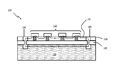
FIG. 1 is a cross-sectional illustration of a MCPCB, in accordance with a
first
exemplary embodiment of the present disclosure.
5
CA 03109659 2021-02-12
WO 2020/036998 PCT/US2019/046410
FIG. 2 is a cross-sectional illustration of a MCPCB, in accordance with the
first
exemplary embodiment of the present disclosure.
FIG, 3 is an illustration of an electronically-activated product having the
MCPCB, in
accordance with the first exemplary embodiment of the present disclosure.
FIG. 4 is a graph illustrating a test of the MCPCB, in accordance with the
first
exemplary embodiment of the present disclosure.
FIG. 5 is a flowchart illustrating a method of generating an ultra-narrow,
high-
current pulse driver with a MCPCB, in accordance with the first exemplary
embodiment of
the present disclosure.
The present disclosure relates to a method of designing and fabricating
printed
circuit boards (PCBs) for products which must generate high-current pulses
with ultra-
narrow temporal widths. In accordance with this disclosure, a high-current
pulse is generally
characterized as a pulse with a greater than 50 amperes peak and an ultra-
narrow temporal
width is generally characterized as less than 10 nanoseconds. Electrical
current pulses of
this type are generally Gaussian in shape and are therefore defined by their
full-wave at half
maximum (FWIIM) pulse width.
More specifically, the present disclosure includes the use of Metal-Core
Printed
Circuit Boards (MCPCB) in ultra-narrow, high-current pulse generation. FIG. 1
is a cross-
sectional illustration of a MCPCB 100, in accordance with a first exemplary
embodiment of
the present disclosure. As shown, the MCPCB 100 includes a rigid, metal heat
sink 110,
which may be formed from copper, aluminum, or other known heat sink materials.
A
dielectric layer .120 is positioned directly in contact with the rigid, metal
heat sink 110. This
dielectric layer 120 is electrically insulating and may be formed from a
polymer. The
electrically conductive top layer 130 contains at least one conductive trace
as well circuit
components and is positioned at least partially over the dielectric layer 120.
The dielectric
layer 120 has a thickness of less than 0.007 inches.
The dielectric layer 120, or dielectric layers, is bonded directly to the
rigid, metal
heat sink 110, with the conductive top layer 130 or copper layer bonded on the
dielectric
layer 120. Various circuitry components 160 are positioned in electrical
communication
with the conductive top layer 130 such that a high current path 170 can be
formed between
the circuitry components 160, through one or more vias 180 positioned between
the
6
CA 03109659 2021-02-12
WO 2020/036998 PCT/US2019/046410
conductive top layer130, through the dielectric layer 120 and to the rigid,
metal heat sink
1.10. The MCPCB 100 of FIG. 1 is used in applications where the heat sink 110
does not
require electrical isolation from the current.
FIG. 2 is a cross-sectional illustration of a MCPCB, in accordance with the
first
exemplary embodiment of the present disclosure. In particular, FIG. 2
illustrates the
MCPCB 100 for use in an application where the heat sink 110 requires
electrical isolation
from the circuit. As shown, the MCPCB 100 includes a rigid, metal heat sink
110, which
may be formed from copper, aluminum, or other known heat sink materials. A
polymer
dielectric layer 124 or pre-preg polymer dialectic layer, or multiple layers
thereof, is
positioned in contact with the heat sink 110. One or more polymer dielectric
layers 124 are
formed from a polymer dielectric material. Next, the dielectric layer 120 is
positioned
between the conductive top layerl 30 which is =formed from a conductive top
layer 130A and
a conductive bottom layer 13013. This dielectric layer 120 is a core layer
which may be
formed from a polymer dielectric material. The top layer 130A of the
electrically conductive
top layer 130 is position at least partially over the dielectric layer 120,
whereas the bottom
layer 1308 is positioned below the dielectric layer 120. The dielectric layer
120 has a
thickness of less than. 0.007 inches.
The dielectric layer 120 is positioned between the top and bottom layers 130A,
13013
and the overall structure is separated from the metal heat sink with the
polymer dielectric
layer 124. In this structure, various circuitry components 160 can be
positioned in electricai
communication with the top layer 130A such that a high current path 170 can be
formed
between the circuitry components 160, through one or more via.s 180 positioned
between the
top layer 130A of the electrically conductive top layer 130, through the
dielectric layer 120
and to the bottom layer 13013 of the electrically conductive top layer 130.
The heat sink 110
remains in electrical isolation from the current through the polymer
dielectric layer 124,
which allows the MCPCB 100 of FIG. 2 to be used in applications where the heat
sink 110
does require electrical isolation from the current.
The resulting structure of the MCPCBs in FIGS. 1-2 is one where the dielectric
layer
120 can be made thinner than conventional dielectric layers while reducing the
inductance of
the PCB traces. This benefit is due to the fact that the single biggest
contributor to parasitic
circuit inductance is usually the PCB itself. Specifically, the mutual
inductance of PCB
7
CA 03109659 2021-02-12
WO 2020/036998 PCT/US2019/046410
traces can be calculated based on a function of the dielectric constant of the
dielectric layer
120 and the difference between the separation distance of the two conductor
planes and the
width of the conductor planes. Minimizing the dielectric thickness between
supply current
trace and return current trace will reduce the parasitic circuit inductance,
but doing so will
leave the PCB less structurally rigid and durable than is optimal. As a
result, conventionally,
there are minimal requirements for the thickness of the dielectric layer.
However, the subject
disclosure is able to use a dielectric layer 120 that is far thinner than
conventional layers.
This is due to the fact that the rigid, metal heat sink layer 110 provides the
necessary rigidity
and support to the PCB, thus allowing the dielectric layer 120 to be thinned
to significantly
reduce the parasitic circuit inductance. The end product is a MCPCB 100 which
has superior
operating characteristics to conventional MCPCBs without increasing the
overall size of the
PCB or the cost of manufacture.
It is noted that in addition to the MCPCB dielectric layer 120 being much
reduced in
height, a high-current driver is also able to operate at relatively high
average power levels
without the additional use of subsequent heat sinking components, such as
external heat
sinks, thermal pads, greases, and clips. Referring to FIG. 1, the at
conductive top layer 130,
or in reference to FIG. 2, the conductive top and bottom layers 130A, 130B,
may further
include a copper layer formed as a solid copper plane or formed as a structure
with one or
more planar surfaces.
The dielectric layer 120 of the MCPCB 100 may include a variety of different
materials. In one example, the dielectric layer 120 is formed from at least
one of a plurality
of dielectric polymers having a lower dielectric constant (pi) than FR-4. As
is known in the
art, FR-4 is a National Electrical Manufacturers Association (NEMA) grade
designation for
glass-reinforced epoxy laminate material. FR-4 is a composite material
composed of
woven fiberglass cloth with an epoxy resin binder and is commonly used as an
electrical
insulator possessing considerable mechanical strength. The material is known
to retain its
high mechanical values and electrical insulating qualities, and therefore it
is used in a wide
variety of electrical and mechanical applications, including as dielectric
layers in PCBs.
The thickness of conventional dielectric layers is commonly required to be at
least
0.007 inches. In the subject disclosure, the thickness of the dielectric layer
120 is less than
0.007 inches. In one example, the dielectric layer 120 has a thickness of
between 0,006
8
CA 03109659 2021-02-12
WO 2020/036998 PCT/US2019/046410
inches to 0.002. inches. In another example, the dielectric layer 120 has a
thickness of
between 0,002 inches and 0.001 inches, In another example, the dielectric
layer 120 has a
thickness of less than 0.001 inches. In other examples, the dielectric layer
120 may have
other thicknesses less than 0.007 inches, as may vary depending on design and
application
of the MCPCB.
The MCPCB 100 may be incorporated and used within a variety of electronic and
electronically-activated products. FIG, 3 is an illustration of an
electronically-activated
product 140 having the MCPCB 100, in accordance with the first exemplary
embodiment of
the present disclosure. As shown in FIG. 3, the electronically-activated
product 140 includes
the MCPCB 100 therein or otherwise in electrical communication therewith,
Additionally,
the electronically-activated product 140 may include an internal power source
150; however
external power sources may also be used. The electronically-activated product
140 may
include an imaging device, such as a LIDAR source, a gated imaging device, or
a 3D
sensing device, among other imaging devices. Additionally, the electronically-
activated
product 140 may be a pulsed optical illumination source, such as with beacon
lights or range
finding devices, or any other electronic product with a PCB, all of which are
considered
within the scope of the present disclosure.
It is noted that MCPCBs have been used for electronics as a thermal management
technique, especially for LED lighting applications. The MCPCB provides
effective heat
.20 sinking for high power-dissipating components without the use of
additional heat sinks,
thermal pads, greases, clips, etc. However, the application of the MCPCB to
increase
electrical performance, as taught in the subject disclosure, is not known in
the art. Indeed,
the application of the MCPCB to increase electrical performance as specified
herein takes
advantage of the MCPCB construction to dramatically reduce the inductance of
the PCB
traces by utilizing the relatively thick heat sink layer on which the MCPCB is
constructed.
This heat sink is inherently rigid and therefore, it can provide the necessary
structural
support to the MCPCB without a conventionally thick dielectric layer. This
allows a
reduction of the dielectric layer thickness (d) without compromising the
structural integrity
of the MCPCB. Many polymers are commercially available with thickness of only
0.0013
inches, for example. Additionally, the since MCPCB does not depend on the
dielectric
layers for rigidity, it can be constructed using a variety of dielectric
materials. Special
9
CA 03109659 2021-02-12
WO 2020/036998 PCT/US2019/046410
polymers can be used which have lower dielectric constant GO than FR-4 so that
trace
inductance is reduced even further.
FIG. 4 is a graph illustrating a test of the MCPCB, in accordance with the
first
exemplary embodiment of the present disclosure. In particular, the graph of
FIG. 4
illustrates a test comparison between a conventional PCB assembly and a MCPCB
constructed in accordance with this disclosure. The two PCB assemblies were
constructed;
one using the common FR-4 dielectric having a thickness of 0.007 inches as a
dielectric
layer and the other using a. MCPCB with a Sekisui KNDJ002 having a thickness
of 0.003
inches as a dielectric layer. Both PCBs were assembled using the same circuit
components
and tested using the same test stimulus. FWBIM pulse width was measured in
both cases
and came to 15 0.5 nanoseconds. As shown in FIG. 4, in the noted time period,
the resulting
peak current of the MCPCB reached over 100 amperes while the conventional PCB
reached
short of 60 amperes. Thus, the MCPCB was 76% higher over the conventional PCB,
which
illustrates the dramatic performance improvement of the MCPCB of the subject
disclosure
over conventional PCBs.
FIG. 5 is a flowchart 200 illustrating a method of generating an ultra-narrow,
high-
current pulse driver with a MCPCB, in accordance with the first exemplary
embodiment of
the present disclosure. It should be noted that any process descriptions or
blocks in flow
charts should be understood as representing modules, segments, portions of
code, or steps
that include one or more instructions for implementing specific logical
functions in the
process, and alternate implementations are included within the scope of the
present
disclosure in which functions may be executed out of order from that shown or
discussed,
including substantially concurrently or in reverse order, depending on the
functionality
involved, as would be understood by those reasonably skilled in the art of the
present
disclosure.
As is shown by block 202, a MCPCB is provided, wherein the MCPCB has; a rigid,
metal heat sink layer; at least one electrically conductive top layer; at
least one electrically
insulating dielectric layer positioned between the conductive top layer and
the rigid, metal.
heat sink, wherein the dielectric layer has a thickness of less than 0.007
inches. A voltage is
applied to the at least one copper trace of the MCPCB, thereby generating an
ultra-narrow,
CA 03109659 2021-02-12
WO 2020/036998 PCT/US2019/046410
high-current pulse (block 204). The method may include any number of
additional steps,
features, and functions, including any disclosed within the present
description.
It should be emphasized that the above-described embodiments of the present
disclosure, particularly, any "preferred" embodiments, are merely possible
examples of
implementations, merely set forth for a clear understanding of the principles
of the
disclosure. Many variations and modifications may be made to the above-
described
embodiment(s) of the disclosure without departing substantially from the
spirit and.
principles of the disclosure. All such modifications and variations are
intended to be
included herein within the scope of this disclosure and the present disclosure
and protected
by the following claims.
11