Note: Descriptions are shown in the official language in which they were submitted.
1
DRIVE CIRCUIT FOR A LIGHT-EMITTING DIODE LIGHT SOURCE
[0001]
BACKGROUND
[0002] Light-emitting diode (LED) light sources (e.g., LED light engines)
are replacing
conventional incandescent, fluorescent, and halogen lamps as a primary form of
lighting devices.
LED light sources may comprise a plurality of light-emitting diodes mounted on
a single structure
and provided in a suitable housing. LED light sources may be more efficient
and provide longer
operational lives as compared to incandescent, fluorescent, and halogen lamps.
An LED driver
control device (e.g., an LED driver) may be coupled between a power source,
such as an
alternating-current (AC) power source or a direct-current (DC) power source,
and an LED light
source for regulating the power supplied to the LED light source. For example,
the LED driver may
regulate the voltage provided to the LED light source, the current supplied to
the LED light source,
or both the current and voltage.
[0003] Different control techniques may be employed to drive LED light
sources including,
for example, a current load control technique and a voltage load control
technique. An LED light
source driven by the current load control technique may be characterized by a
rated current (e.g.,
approximately 350 milliamps) to which the magnitude (e.g., peak or average
magnitude) of the
current through the LED light source may be regulated to ensure that the LED
light source is
illuminated to the appropriate intensity and/or color. An LED light source
driven by the voltage load
control technique may be characterized by a rated voltage (e.g., approximately
15 volts) to which the
voltage across the LED light source may be regulated to ensure proper
operation of the LED light
source. If an LED light source rated for the voltage load control technique
includes multiple parallel
strings of LEDs, a current balance regulation element may be used to ensure
that the parallel strings
have the same impedance so that the same current is drawn in each of the
parallel strings.
[0004] The light output of an LED light source may be dimmed. Methods for
dimming an
LED light source may include, for example, a pulse-width modulation (PWM)
technique and a
constant current reduction (CCR) technique. In pulse-width modulation dimming,
a pulsed signal with
a varying duty cycle may be supplied to the LED light source. For example, if
the LED light source is
being controlled using a current load control technique, the peak current
supplied to the LED light
Date Recue/Date Received 2022-06-07
2
source may be kept constant during an on-time of the duty cycle of the pulsed
signal. The duty cycle
of the pulsed signal may be varied, however, to vary the average current
supplied to the LED light
source, thereby changing the intensity of the light output of the LED light
source. As another
example, if the LED light source is being controlled using a voltage load
control technique, the
voltage supplied to the LED light source may be kept constant during the on-
time of the duty cycle of
the pulsed signal. The duty cycle of the load voltage may be varied, however,
to adjust the intensity
of the light output. Constant current reduction dimming may be used if an LED
light source is being
controlled using the current load control technique. In constant current
reduction dimming, current
may be continuously provided to the LED light source. The DC magnitude of the
current provided to
the LED light source, however, may be varied to adjust the intensity of the
light output.
[0005] Examples of LED drivers are described in U.S. Patent No. 8,492,987,
issued
July 23, 2013, entitled LOAD CONTROL DEVICE FORA LIGHT-EMITTING DIODE LIGHT
SOURCE; U.S. Patent No. 9,655,177, issued May 16, 2017, entitled FORWARD
CONVERTER
HAVING A PRIMARY-SIDE CURRENT SENSE CIRCUIT; and U.S. Patent No. 9,247,608,
issued
January 26, 2016, entitled LOAD CONTROL DEVICE FOR A LIGHT-EMITTING DIODE
LIGHT
SOURCE.
SUMMARY
[0006] Methods and apparatus are described herein for controlling an LED
light source. A
controllable impedance circuit may be coupled in series with the LED light
source and configured to
conduct a load current through the LED light source. A first switching device
may be connected in series
with the controllable impedance circuit while a feedback circuit is configured
to generate a feedback
signal indicative of a magnitude of the load current conducted through the LED
light source. The
feedback circuit may be coupled to a control loop circuit configured to
generate a drive signal for
controlling the controllable impedance circuit based on the feedback signal.
The control loop circuit
may comprise a second switching device and/or a filter circuit. The second
switching device may be
capable of being rendered conductive and non-conductive to control when the
feedback signal is
used to generate the drive signal (e.g., after the feedback signal is passed
through the filter circuit).
[0007] A digital control circuit may control the control loop circuit to
adjust a peak
magnitude of the load current conducted through the LED light source toward a
target magnitude.
The digital control circuit may render the first switching device conductive
and non-conductive via a
pulse-width modulated (PWM) signal and adjust a duty cycle of the PWM signal
to adjust an
average magnitude of the load current. The digital control circuit may further
render the second
switching device conductive and non-conductive in coordination with the PWM
signal. For example,
the digital control circuit may be configured to render the second switching
device conductive at the
Date Recue/Date Received 2022-06-07
3
end of a first time period after the digital control circuit renders the first
switching device
conductive, and the digital control circuit may be further configured to
render the second switching
device non-conductive at the beginning of a second time period before the
digital control circuit
renders the first switching device non-conductive.
[0008] The control loop circuit described herein may comprise an integrator
circuit. The
control loop circuit may receive a target current control signal from the
digital control circuit and
generate the drive signal by integrating the difference between the target
current control signal and
the feedback signal via the integrator circuit. The control loop circuit may
be characterized by a
time constant that is greater than a load current period of the load current
conducted by the
controllable impedance circuit.
[0009] One or more of the components and/or functions described herein may
be
implemented digitally. For example, sampling of the feedback signal may be
controlled by a digital
control circuit and filtering operations may be conducted using a digital low -
pass filter.
BRIEF DESCRIPTION OF THE DRAWINGS
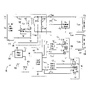
[0010] Fig. 1 is a simplified block diagram of a controllable electrical
device, such as a
controllable light source.
[0011] Fig. 2 is a simplified schematic diagram of a drive circuit, such as
a light-emitting diode
(LED) drive circuit, and a control loop circuit of an electrical device, such
as the controllable light
source of Fig. 1.
[0012] Fig. 3 are example plots of the relationships between various
operating parameters of the
controllable light source of Fig. 1 and a target intensity of the controllable
ligjht source.
[0013] Figs. 4A-4C are diagrams of simplified wavefollais illustrating the
operation of the
drive circuit and the control loop circuit of Fig. 2.
[0014] Fig. 5 is a simplified flow diagram of an example control procedure
for controlling the
control loop circuit of Fig. 2.
[0015] Fig. 6 is a simplified schematic diagram of a circuit that may be
used to realize the
functionality of the drive circuit and the control loop circuit shown in Fig.
2.
[0016] Fig. 7 is a simplified flow diagram of an example control procedure
for controlling the
circuit shown in Fig. 6.
Date Recue/Date Received 2022-06-07
4
DETAILED DESCRIPTION
[0017] Fig. 1 is a simplified block diagram of a controllable electrical
device, such as a
controllable lighting device 100 (e.g., a controllable light source). For
example, the controllable
lighting device 100 may be a lamp that comprise one or more light sources,
such as light-emitting
diode (LED) light sources 102, 104 (e.g., LED light engines). The LED light
sources 102, 104 may
be controlled to adjust an intensity and/or a color (e.g., a color
temperature) of a cumulative light
output of the controllable lighting device 100. Each LED light source 102, 104
is shown in Fig. 1 as
a plurality of LEDs connected in series but may comprise a single LED or a
plurality of LEDs
connected in parallel or a suitable combination thereof, depending on the
particular lighting system.
In addition, each LED light source 102, 104 may comprise one or more organic
light-emitting diodes
(OLEDs). The controllable lighting device 100 may include a plurality of
different LED light
sources, which may be rated at different magnitudes of load current and
voltage. While not shown in
Fig. 1, the controllable lighting device 100 may comprise a housing (e.g., a
translucent housing) in
which the LED light sources are located and through which the LED light
sources may shine. For
example, the controllable lighting device 100 may be capable of providing wann-
dimming such that
the color temperature of the cumulative light output shifts towards a wann-
white color temperature
as the intensity of the cumulative light output is decreased. For example, the
first LED light source
102 may comprise a white LED light source and the second LED light source 104
may comprise a
warm-white (e.g., red) LED light source, and the first LED light source 102
may have a higher
power rating than the second LED light source 104.
[0018] The controllable lighting device 100 may be a screw-in LED lamp
configured to be
screwed into a standard Edison socket. The controllable light device 100 may
comprise a screw-in
base that includes a hot connection H and a neutral connection N for receiving
an alternating-current
(AC) voltage VAC from an AC power source (not shown). The hot connection H and
the neutral
connection N may also be configured to receive a direct-current (DC) voltage
from a DC power
source. The controllable lighting device 100 may comprise a radio-frequency
interference (RFI) filter
and rectifier circuit 110, which may receive the AC voltage VAC. The RFI
filter and rectifier circuit
110 may operate to minimize the noise provided on the AC power source and to
generate a rectified
voltage VRECT.
[0019] The controllable lighting device 100 may comprise a power converter
circuit 120, such
as a flyback converter, which may receive the rectified voltage VRECT and
generate a variable
direct-current (DC) bus voltage VBus across a bus capacitor CBus. The power
converter circuit 120
may comprise other types of power converter circuits, such as, for example, a
boost converter, a buck
converter, a buck-boost converter, a single-ended primary-inductance converter
(SEPIC), a auk
Date Recue/Date Received 2022-06-07
5
converter, or any other suitable power converter circuit for generating an
appropriate bus voltage. The
power converter circuit 120 may provide electrical isolation between the AC
power source and the
LED light source 102, 104 and may operate as a power factor correction (PFC)
circuit to adjust the
power factor of the controllable lighting device 100 towards a power factor of
one.
[0020] As shown in Fig. 1, the flyback converter 120 may comprise a flyback
transformer 122, a field-effect transistor (FET) Q123, a diode D124, a
resistor R125, a resistor R126,
a flyback control circuit 127, and/or a feedback resistor R128. The flyback
transformer 122 may
comprise a primary winding and a secondary winding. The primary winding may be
coupled in series
with the FET Q123. Although illustrated as the FET Q123, any switching
transistor or other suitable
semiconductor switch may be coupled in series with the primary winding of the
flyback transformer
122. The secondary winding of the flyback transformer 122 may be coupled to
the bus capacitor CBus
via the diode D124. A bus voltage feedback signal VBUS-FB may be generated,
e.g., by a voltage
divider comprising the resistors R125, R126 coupled across the bus capacitor
CBus. The flyback
control circuit 127 may receive the bus voltage feedback signal VBus-FB and a
control signal
representative of the current through the FET Q123 from the feedback resistor
R128, which may be
coupled in series with the FET Q123. The flyback control circuit 127 may
control the FET Q123 to
selectively conduct current through the flyback transformer 122 to generate
the bus voltage VBus.
The flyback control circuit 127 may render the FET Q123 conductive and non-
conductive, for
example, to control the magnitude of the bus voltage VBUS towards a target bus
voltage VBUS-
TRGT in response to the DC magnitude of the bus voltage feedback signal VBus-
FB and the
magnitude of the current through the FET Q123.
[0021] The controllable lighting device 100 may comprise one or more load
regulation
circuits, such as LED drive circuits 130, 140, for controlling power delivered
to (e.g., the intensities
of) the LED light sources 102, 104, respectively. The LED drive circuits 130,
140 may each receive
the bus voltage VBus and may adjust magnitudes of respective load currents
LOAD', ILOAD2
conducted through the LED light sources 102, 104 and/or magnitudes of
respective load voltages
VLOAD1, VLOAD2 generated across the LED light sources. One or more of the LED
drive circuits
130, 140 may comprise a controllable-impedance circuit, such as a linear
regulator, for example, as
described herein. One or more of the LED drive circuits 130, 140 may comprise
a switching regulator,
such as a buck converter for example. Examples of various embodiments of LED
drive circuits are
described in U.S. Patent No. 8,492,987, filed July 23, 2013, and U.S. Patent
No. 9,253,829, issued
February 2,2016, both entitled LOAD CONTROL DEVICE FOR A LIGHT-EMITTING DIODE
LIGHT SOURCE.
Date Recue/Date Received 2022-06-07
6
[0022] The controllable lighting device 100 may comprise a control circuit
150 for
controlling the LED drive circuits 130, 140 to control the magnitudes of the
respective load currents
ILOAD1, ILOAD2 conducted through the LED light sources 102, 104 to adjust the
respective
intensities of the LED light sources. The control circuit 150 may be
configured to turn both of the
LED light sources 102, 104 on and off to turn the controllable lighting device
100 on and off,
respectively. The control circuit 150 may be configured to control the
respective intensities of the
LED light sources 102, 104 to control the intensity and/or the color (e.g.,
the color temperature) of
the cumulative light emitted by the controllable lighting device 100. The
control circuit 150 may be
configured to adjust (e.g., dim) a present intensity LPRES of the cumulative
light emitted by the
controllable lighting device 100 towards a target intensity LTRGT, which may
range across a
dimming range of the controllable light source, e.g., between a low-end
intensity LLE (e.g., a
minimum intensity, such as approximately 0.1% - 1.0%) and a high-end intensity
LHE (e.g., a
maximum intensity, such as approximately 100%). The control circuit 150 may be
configured to
adjust a present color temperature TPRES of the cumulative light emitted by
the controllable
lighting device 100 towards a target color temperature TTRGT, which may range
between a cool-
white color temperature (e.g., approximately 3100-4500 K) and a warm-white
color temperature
(e.g., approximately 2000-3000 K).
[0023] The control circuit 150 may comprise a digital control circuit 152,
such as, for
example, a microprocessor, a microcontroller, a programmable logic device
(PLD), an application
specific integrated circuit (ASIC), a field-programmable gate array (FPGA), or
any other suitable
processing device or controller. The control circuit 150 may comprise a memory
(not shown)
configured to store operational characteristics of the controllable lighting
device 100 (e.g., the target
intensity LTRGT, the target color temperature TTRGT, the low-end intensity
LLE, the high-end
intensity LHE, etc.). The memory may be implemented as an external integrated
circuit (IC) or as an
internal circuit of the digital control circuit 152. The controllable lighting
device 100 may comprise a
power supply 160 that may be coupled to a winding 162 of the flyback
transformer 122 of the power
converter circuit 120 and may be configured to generate a supply voltage Vcc
for powering the
digital control circuit 152 and other low-voltage circuitry of the
controllable lighting device.
[0024] The control circuit 150 may also comprise control loop circuits
(e.g., analog control
loop circuits) 154, 156 for controlling the LED drive circuits 130, 140,
respectively. The LED drive
circuits 130, 140 may comprise respective regulation devices (e.g., regulation
field-effect transistors
(FET) Q132, Q142) coupled (e.g., in series) with the LED light sources 102,
104, respectively, for
conducting the load currents ILOAD1, ILOAD2. Each regulation FET Q132, Q142
may comprise any
type of suitable power semiconductor switch, such as, for example, a bipolar
junction transistor
Date Recue/Date Received 2022-06-07
7
(BJT), and/or an insulated-gate bipolar transistor (IGBT). The control loop
circuits 154, 156 may
generate respective drive signals VDR1, VDR2 that may be received by gates of
the regulation FETs
Q132, Q142 for controlling the regulation FETs in the linear region to provide
controllable
impedances in series with the LED light sources 102, 104, respectively (e.g.,
to operate the regulation
FETs Q132, Q142 as linear regulators). When the regulation FETs Q132, Q142 are
conducting the
respective load currents ILOAD', ILOAD2, respective regulator voltages VR1,
VR2 may be
developed across the regulation FETs Q132, Q142.
[0025] The regulation FETs Q132, Q142 may be coupled (e.g., in series) with
respective
feedback circuits (e.g., current feedback (CFB) circuits) 134, 144. The
current feedback circuits 134,
144 may be coupled to the control loop circuits 154, 156 of the control
circuit 150 and may generate
respective current feedback signals VF1, VFB2, which may be received by the
control loop circuits 154,
156. The control loop circuits 154, 156 may be configured to adjust the
magnitudes (e.g., DC
magnitudes) of the drive signals VDR1, VDR2 provided to the gates of the
regulation FETs Q132,
Q142 in response to the magnitudes of the current feedback signals VFB1, VFB2,
respectively. The
digital control circuit 152 may generate respective target-current control
signals VTRGT1, VTRGT2,
which may also be received by the control loop circuits 154, 156. The control
loop circuits 154, 156
may be configured to adjust the magnitudes of the drive signals VDR1, VDR2
provided to the gates of
the regulation FETs Q132, Q142 to control the magnitudes of the load current
LOAD', ILOAD2
towards respective target current ITRGT1, ITRGT2 that are set by the target-
current control signals
VTRGT1, VTRGT2.
[0026] The LED drive circuits 130, 140 may further comprise dimming devices
(e.g., dimming
FETs Q136, Q146 or another type of semiconductor switches) coupled (e.g., in
series) with the
regulation FETs Q132, Q142 and the current feedback circuits 134, 144,
respectively. The digital control
circuit 152 may generate respective dimming control signals VDIM1, VDIM2 that
may be received by
gates of the respective dimming FETs Q136, Q146 for rendering the dimming FETs
conductive and non-
conductive to adjust average magnitudes of the load currents ILoAD1, ILoAD2,
respectively. For
example, the digital control circuit 152 may be configured to pulse-width
modulate (PWM) the load
currents ILoADI, ILOAD2 by generating the dimming control signals VDIM1, VDIM2
as pulse-width
modulated (PWM) signals at a dimming frequency fDIM. The digital control
circuit 152 may be
configured to adjust respective duty cycles DC1, DC2 of the dimming control
signals VDIM1, VDIM2 to adjust the average magnitudes of the load currents
ILOAD1, ILOAD2,
respectively. When the digital control circuit 152 is pulse-width modulating
the dimming control
signals VDIM1, VDIM2, the load currents ILOAD1, ILOAD2 may be characterized by
a load-current
frequency fLoAD (e.g., which is approximately equal to the dimming frequency
fDim of the dimming
Date Recue/Date Received 2022-06-07
8
control signals VDIM1, VDIM2) and a corresponding load-current period TLOAD.
The load-current
frequency fLoAD may be high enough to prevent flickering that may be visible
to the human eye.
[0027] The dimming FETs Q136, Q146 may be coupled between the respective
current
feedback circuits 134, 144 and circuit common. The digital control circuit 152
may be configured to
control when the control loop circuits 154, 156 are responsive to the
respective current feedback signals
VFB1, VFB2 for adjusting the magnitudes of the drive signals VDR1, VDR2. The
digital control circuit
152 may be configured to render the control circuit circuits 154, 156
responsive and nonresponsive to
the respective current feedback signals VFB1, VFB2 in coordination with the
respective dimming
control signals VDIM1, VDIM2. For example, the digital control circuit 152 may
be configured to
enable the control loop circuits 154, 156 to be responsive to the respective
current feedback signals
VFB1, VFB2 during feedback windows TwIN that may be approximately the same
length as or slightly
shorter than the time periods when the dimming FETs Q136, Q146 are rendered
conductive. The digital
control circuit 152 may be configured to render the control loop circuits 154,
156 responsive to the
respective current feedback signals VFB1, VFB2 at approximately the same time
or slightly after the
dimming FETs Q136, Q146 are rendered conductive. The digital control circuit
152 may be configured
to render the control loop circuits 154, 156 non-responsive to the respective
current feedback signals
VFB1, VFB2 at approximately the same time or slightly before the dimming FETs
Q136, Q146 are
rendered non-conductive. To control the operation of the respective control
loop circuits 154, 156, the
digital control circuit 152 may generate respective feedback window control
signals Vw1N1, VwIN2
that may be received by the control loop circuits for enabling and disabling
when the control loop circuits
are responsive to the respective current feedback signals VFB1, VFB2. As a
result, each control loop
circuit 154, 156 may be responsive to a peak magnitude IPK of the respective
current feedback signal
VFB1, VFB2 (e.g., when the dimming FETs Q136, Q146 are conductive).
[0028] The techniques described herein may help prevent erroneous operation
of the
controllable lighting device 100 in various situations. For example, since the
dimming FETs Q136,
Q146 may be coupled between the respective current feedback circuits 134, 144
and the circuit
common, the magnitudes of the current feedback signals VFB1, VFB2 may be
pulled up towards the bus
voltage VBus when the dimming FETs Q136, Q146 are non-conductive, which may
cause the control
loop circuits 154, 156 to incorrectly drive the regulation FETs Q132, Q142. By
configuring the digital
control circuit 152 to control (e.g., at least with respect to timing) when
the control loop circuits 154,
156 are responsive to the respective current feedback signals VFsi, VFB2 for
adjusting the magnitudes
of the drive signals VDR1, VDR2, erroneous generation of the drive signals
VDR1, VDR2 may be
avoided.
Date Recue/Date Received 2022-06-07
9
[0029] The controllable lighting device 100 may comprise a bus adjustment
circuit 170 for
controlling the magnitude of the bus voltage VBUS (e.g., to make sure that the
regulation FETs
Q132, Q142 do not dissipate too much power). For example, the bus adjustment
circuit 170 may be
coupled to the junction of the first regulation FET Q132 and the first LED
light source 102, and may
be responsive to the first regulator voltages VR1 across the first regulation
FET Q132. The bus
adjustment circuit 170 may be coupled to the junction of the resistors R125,
R126 for adjusting the
magnitude of the bus voltage feedback signal VBus-Fs to cause the flyback
control circuit 127 to
adjust the magnitude of the bus voltage VBus. For example, the bus adjustment
circuit 170 may
adjust the magnitude of the bus voltage VBus to control the magnitude of the
first regulator
voltage Viu to be less than a maximum regulator voltage threshold VR-MAX
(e.g., approximately 0.6
volts), for example, to prevent the power dissipated in regulation FETs Q132,
Q142 from becoming
too large. In examples (e.g., as shown in Fig. 1), the bus adjustment circuit
170 may be only coupled
to the first regulation transistor Q132. Since the first LED ligjht source 102
may have a higher power
rating than the second LED light source 104 (as previously mentioned),
adjustments of the magnitude
of the bus voltage VBus in response to the magnitude of the first regulator
voltage VR1 to make sure that
the first regulation FET Q132 does not dissipate too much power may also
ensure that the second
regulation FET Q142 does not dissipate too much power.
[0030] The controllable lighting device 100 may comprise a communication
circuit 180
coupled to the digital control circuit 152. The communication circuit 180 may
comprise a wireless
communication circuit, such as, for example, a radio-frequency (RF)
transceiver coupled to an
antenna 182 for transmitting and/or receiving RF signals. The wireless
communication circuit may
be an RF transmitter for transmitting RF signals, an RF receiver for receiving
RF signals, or an
infrared (IR) transmitter and/or receiver for transmitting and/or receiving IR
signals. The
communication circuit 180 may be coupled to the hot connection H and the
neutral connection N of
the controllable lighting device 100 for transmitting a control signal via the
electrical wiring using,
for example, a power-line carrier (PLC) communication technique. The digital
control circuit 152
may be configured to determine the target intensity LTRGT for the controllable
lighting device 100
in response to messages (e.g., digital messages) received via the
communication circuit 180. The
digital control circuit 152 may be configured to determine respective target
intensities LTRGT1,
LTRGT2 for the LED light sources 102, 104 in response to the determined target
intensity LTRGT
for the controllable lighting device 100.
[0031] When the target intensity LTRGT1, LTRGT2 of at least one of the LED
ligjht sources
102, 104 is greater than or equal to a transition intensity LTRAN, the digital
control circuit 152 may be
configured to render the respective dimming FET Q136, Q146 conductive (e.g.,
conductive at all times)
and adjust the intensity of the respective LED light source using a constant
current reduction (CCR)
Date Recue/Date Received 2022-06-07
10
dimming technique. Using the CCR dimming technique, the digital control
circuit 152 may adjust the
respective target-current control signal VTRGT1, VTRGT2 to cause the
respective control loop circuit
154, 156 to adjust the average magnitude of the load current ILOAD1, ILOAD2
towards the respective
target current ITRGT1, ITRGT2. The target currents ITRGT1, ITRGT2 may each
range between a
maximum current IMAX (e.g., at the high-end intensity Lam) and a minimum
current ImIN (e.g., at the
transition intensity LTRAN).
[0032] When the target intensity LTRGT1, LTRGT2 of at least one of the LED
light sources
102, 104 is less than the transition intensity LTRAN, the digital control
circuit 152 may be configured to
control the respective dimming FET Q136, Q146 to adjust the intensity of the
respective LED light
source using a pulse-width modulation (PWM) dimming technique. For example,
the digital control
circuit 152 may be configured to control the respective target-current control
signal VTRGT1,
VTRGT2 to maintain the respective target current ITRari, ITRGT2 constant.
Using the PWM dimming
technique, the digital control circuit 152 may adjust the duty cycle DCi, DC2
of the respective
dimming control signal VDIMI, VDIM2 to adjust the average magnitude of the
load current LOAD1,
ILOAD2 below the minimum current IMIN. For example, the digital control
circuit 152 may adjust the
duty cycle DCi, DC2 of each of the dimming control signals VDIM1, VDIM2 as a
function of the
respective target intensity LTRGT1, LTRGT2. For example, the digital control
circuit 152 may linearly
decrease the duty cycle DCi, DC2 as the respective target intensity LTRGT1,
LTRGT2 decreases, and
vice versa. Each control loop circuit 154, 156 may continue to regulate the
peak magnitudes IPK of the
load current koAD1, ILOAD2 towards the target current ITRGTi, ITRGT2 when the
respective
dimming FET Q136, Q146 is conductive. Each control loop circuit 154, 156 may
be characterized by a
time constant that is much greater than the load-current period TLOAD of the
respective load
current ILOAD1, ILOAD2, for example, to help avoid changes in the magnitudes
of the respective drive
signals VDR1, VDR2 when the dimming FETs Q136, Q146 are non-conductive. The
time constant may
be associated with one or more integrator circuit and/or RC filter circuits
comprised in the control loop
circuit 154, 156, for example. The value of the time constant may be
determined by the electrical
properties (e.g., capacitance and/or resistance) of one or more components
comprised in the control loop
circuit 154, 156.
[0033] Fig. 2 is a simplified schematic diagram of an LED drive circuit 210
(e.g., one of the
LED drive circuits 130, 140) and a control loop circuit 220 (e.g., one of the
control loop circuits 154,
156) of an electrical device 200, such as an LED driver or a controllable
light source (e.g., the
controllable lighting device 100). The LED drive circuit 210 may be coupled in
series with an LED
light source 202 (e.g., one of the LED light sources 102, 104) for conducting
a load current ILOAD
through the LED light source. The control loop circuit 220 may generate a
drive signal VDR for
controlling the LED drive circuit 210 to adjust a magnitude of the load
current ILOAD through the
Date Recue/Date Received 2022-06-07
11
LED light source. The LED driver 100 may also comprise a digital control
circuit 252 (e.g., the
digital control circuit 152) for generating a PWM control signal (e.g., a
target-current control signal
VTRGT.PWM) that may be received by the control loop circuit 220 for setting a
target current
ITRGT for the load current ILOAD. The digital control circuit 252 may be
configured to adjust the
intensity of the LED light source 202 towards a target intensity LTRGT that
may range between a
minimum intensity LMIN (e.g., approximately 0.1% - 1.0%) and a maximum
intensity LMAX (e.g.,
approximately 100%). The minimum intensity LMIN may be approximately the
lowest intensity at
which the digital control circuit 252 may control the LED light source 202
under steady state conditions
(e.g., when the target intensity LTRGT is being held constant).
[0034] The LED drive circuit 210 may comprise a regulation device such as a
regulation
FET Q212 coupled in series with the LED light source 202. The regulation FET
Q212 may
comprise any type of suitable power semiconductor switch, such as, for
example, a bipolar junction
transistor (BJT), and/or an insulated-gate bipolar transistor (IGBT). When the
regulation FET Q212 is
conductive, a regulator voltage VR may be developed across the regulation FET.
The LED drive
circuit 210 may comprise a current feedback circuit (e.g., a current feedback
resistor 8214) coupled in
series with the regulation FET Q212 for generating a current feedback signal
VFB that may have a
DC magnitude representative of the magnitude of the load current ILOAD. The
LED drive circuit 210
may comprise a dimming device (e.g., such as a dimming FET Q216 or another
type of
semiconductor switch) coupled between the current feedback resistor 8214 and
circuit common. The
digital control circuit 252 may generate a dimming control signal VDIM that
may be received by a
gate of the dimming FET Q216. The dimming FET Q216 may be rendered conductive
and non-
conductive in response to the dimming control signal VDIM for adjusting an
average magnitude of
the load current ILOAD.
[0035] The control loop circuit 220 may receive the current feedback signal
VF B generated by
the current feedback resistor 8214 and/or the PWM target-current control
signal VTRGT-PWM
generated by the digital control circuit 252. The current feedback signal VFB
may be received by a
controllable switch 222 comprised in the control loop circuit 220. The
controllable switch 222 may be
rendered conductive and non-conductive in response to a feedback window
control signal Vwnv (e.g., a
switch control signal) generated by the digital control circuit 252. The
controllable switch 222 may be
coupled to a filter circuit, which may comprise a capacitor C224 and a
resistor 8225. When the
controllable switch 222 is conductive, the capacitor C224 (e.g., having a
capacitance of approximately
1.0 IJF) may charge to approximately a peak magnitude IFK of the current
feedback signal VFB
through the resistor R225 (e.g., having a resistance of approximately 100) for
generating a peak-current
feedback signal VFB-PK across the capacitor.
Date Recue/Date Received 2022-06-07
12
[0036] The control loop circuit 220 may comprise an operational amplifier
U226 comprising
an inverting input coupled to receive the current feedback signal VFB through
a resistor R228. The
control loop circuit 220 may comprise a filter circuit (e.g., a low-pass RC
filter circuit) including a
resistor R230 (e.g., having a resistance of approximately 1 k0) and a
capacitor C232 (e.g., having a
capacitance of approximately 0.1 F). The PWIVI target-current control signal
VTRGT-PWM may be
received by the resistor R230, such that a DC target-current control signal
vIRGT-DC is generated at
the junction of the resistor R230 and the capacitor C232 and has a DC
magnitude representative of
the target current ITRGT for the load current ILOAD. The DC target-current
control signal V1RGT-DC
may be coupled to a non-inverting input of the operational amplifier U226. For
example, the digital
control circuit 252 may generate the PWM target-current control signal VTRGT-
PWM as a pulse-width
modulated signal having a duty cycle DCTRGT representative of the target
current IlRGT for the load
current ILOAD. In addition, the digital control circuit 252 may comprise a
digital-to-analog converter
(DAC) for generating the DC target-current control signal VTRGT-Dc that may be
directly coupled
to the non-inverting input of the operational amplifier U226 (e.g., without
requiring the resistor R230
and the capacitor C232).
[0037] The control loop circuit 220 may comprise a capacitor C234 coupled
between the
inverting input and an output of the operational amplifier U226, such that the
control loop circuit
220 may be configured to integrate the error between the peak-current feedback
signal VFB-PK and
the DC target-current control signal VIRGT-DC. The control loop circuit 220
may generate the drive
signal VDR that may be received by a gate of the regulation FET Q212 for
controlling the regulation
FET in the linear region to provide a controllable impedance in series with
the LED light source 202
(e.g., the regulation FET may be operated as a linear regulator). The output
of the operational
amplifier U226 may be coupled to the gate of the regulation FET Q212 through
another filter circuit
(e.g., a low-pass RC filter circuit) including a resistor R236 (e.g., having a
resistance of
approximately 1 kil) and a capacitor C238 (e.g., having a capacitance of
approximately 0.1 F).
[0038] The digital control circuit 252 may control the dimming control
signal VDIM to
render the dimming FET Q216 conductive and non-conductive to adjust average
magnitude of the
load current ILOAD. For example, the digital control circuit 252 may be
configured to pulse -width
modulate (PWM) the load current ILOAD by generating the dimming control signal
VDIM as a pulse-
width modulated (PWM) signal at a dimming frequency fDIM. The digital control
circuit 252 may
be configured to adjust a duty cycle DCDIM of the dimming control signal VDIM
to adjust the
average magnitude of the load current ILOAD. When the digital control circuit
252 is pulse -width
modulating the dimming control signal VDIM, the load current ILOAD may be
characterized by a
load-current frequency fLoAD that is approximately equal to the dimming
frequency of the
Date Recue/Date Received 2022-06-07
13
dimming control signal VDIM. The load-current frequency fLoAD may be high
enough to prevent
flickering in the LED light source 202 that may be visible to the human eye.
[0039] The digital control circuit 252 may be configured to render the
controllable switch
222 conductive and non-conductive in coordination with the dimming control
signal VDIM. For
example, the digital control circuit 252 may be configured to render the
controllable switch 222
conductive at approximately the same time or slightly after the digital
control circuit renders the
dimming FET Q216 conductive. The digital control circuit 252 may be configured
to render the
controllable switch 222 non-conductive at approximately the same time or
slightly before the digital
control circuit renders the dimming FET Q216 non-conductive. This way, the
magnitude of the peak-
current feedback signal VFB-PK may be representative of a peak magnitude IFK
of the load current
ILOAD, which may prevent erroneous operation of the control circuitry in
various situations. For
example, since the dimming FET Q216 may be coupled between the current
feedback resistor R214
and circuit common, the magnitude of the current feedback signals VFB may be
pulled up towards
the bus voltage VBus when the dimming FET Q216 is non-conductive. This may
cause the control
loop circuit 220 to incorrectly drive the regulation FETs Q212. By configuring
the digital control
circuit 252 to control when the controllable switch 222 is rendered
conductive, erroneous generation
of the drive signal VDR may be avoided.
[0040] The digital control circuit 252 may control the duty cycle DCTRGT of
the PWM target-
current control signal VTRGT-PWM, the duty cycle DCDnvi of the dimming control
signal VDIM, and/or the
dimming frequency fDim of the dimming control signal VDIM as a function of the
target intensity
LTRGT. Fig. 3 shows example plots of the relationship between the peak current
IPK of the load current
ILOAD and the target intensity LTRGT, the relationship between the duty cycle
DCDIM of the dimming
control signal VDIM and the target intensity LTRGT, and the relationship
between the dimming
frequency fDim of the dimming control signal VDIM and the target intensity
LTRGT.
[0041] When the target intensity LTRGT of the LED light source 202 is
greater than or equal to
a transition intensity LTRAN, the digital control circuit 252 may be
configured to render the dimming
FET Q216 conductive (e.g., conductive at approximately all times) and adjust
the peak magnitude IPK
of the load current ILOAD to adjust the intensity of the LED light source
(e.g., using a constant current
reduction (CCR) dimming technique). For example, the digital control circuit
252 may adjust the duty
cycle DCTRGT of the PWM target-current control signal VTRGT-PWM to cause the
control loop
circuit 220 to adjust the peak magnitude IPK of the load current ILOAD towards
the target current
ITRGT, which may range between a maximum current IMAx and a minimum current
IMIN. When the
target intensity LTRGT of the LED light source 202 is greater than or equal to
the transition intensity
LTRAN, the duty cycle DCDIM of the dimming control signal VDIM may be held
constant at a
Date Recue/Date Received 2022-06-07
14
maximum duty cycle DCmAx. The maximum duty cycle DCmAx may be less than 100%
(e.g., as
shown in Fig. 3), such that the digital control circuit 252 may pulse-width
modulate the load current
ILOAD. The maximum duty cycle DCmAx may be equal to 100%, such that the
dimming FET Q216
may be conductive at all times when the target intensity LTRGT of the LED
light source 202 is greater
than or equal to the transition intensity LTRAN.
[0042] When the target intensity LTRGT of the LED light source 202 is less
than the transition
intensity LTRAN, the digital control circuit 252 may be configured to control
the dimming FET Q216 to
adjust the intensity of the LED ligjht source (e.g., using a pulse-width
modulation (PWM) dimming
technique). When using the PWM dimming technique, the digital control circuit
252 may be configured
to maintain the duty cycle DCTRGT of the target-current control signal VTRGT-
PWM constant to
maintain the target current ITRGT constant, and adjust the duty cycle DCDIA4
of the dimming control
signal VDIM to adjust the magnitude of the load current ILOAD. For example,
the digital control circuit
252 may adjust the duty cycle DCDTh4 as a function of the target intensity
LTRGT (e.g., linearly) as
shown in Fig. 3. The control loop circuit 220 may continue to regulate the
peak magnitude IPK of the
load current ILOAD towards the target current ITRGT when the dimming FET Q216
is conductive. The
control loop circuit 220 may be characterized by a time constant that is much
greater than the load-
current period TLOAD of the load current ILOAD, for example, to help avoid
changes in the magnitude
of the drive signal VDR when the dimming FET Q216 is non-conductive.
[0043] The digital control circuit 252 may be configured to fade (e.g.,
gradually adjust over a
period of time) the target intensity LTRGT (and thus the present intensity) of
the LED light
source 202. The digital control circuit 252 may be configured to fade the LED
light source 202 from off
to on by slowly increasing the present intensity LPRES of the LED light source
from a minimum fading
intensity LFADE-MIN, which may be less than the minimum intensity LMIN (e.g.,
such as
approximately 0.02%), to the target intensity LTRGT. The digital control
circuit 252 may be configured
to fade the LED light source 202 from on to off by slowly decreasing the
present intensity LPRES of the
LED light source from an initial intensity greater than or equal to the
minimum intensity LMIN to the
minimum fading intensity LFADE-MIN at which point the digital control
circuit 252 may turn off the LED light source. As shown in Fig. 3, when the
target intensity LTRGT is
less than the minimum intensity LIAM, the digital control circuit 252 may
adjust the dimming frequency
fDim of the dimming control signal VDIM with respect to the target current
ITRGT (e.g., while holding
the duty cycle DCTRGT of the target-current control signal VTRGT-PWM and the
duty cycle DCDim of
the dimming control signal VDIM constant).
[0011] Figs. 4A-4C show waveforms that illustrate the operation of the LED
drive
Date Recue/Date Received 2022-06-07
15
circuit 210 and the control loop circuit 220 of Fig. 2. In the example shown
in Fig. 4A, the target intensity
LTRGT may be equal to and/or close to the maximum intensity LmAx. The peak
current IN( of the load
current ILOAD may be controlled to the maximum current ImAx. The duty cycle
DCDim of the dimming
control signal VDIM may be controlled to the maximum duty cycle DCmAx (e.g.,
at 99%) resulting in
prolonged on time ToN of the dimming control signal. The digital control
signal 252 may drive the
window control signal VwIN high towards the supply voltage Vcc after a first
offset time period
TOFFSET1 from when the dimming control signal VDIM is driven high. The digital
control signal 252
may drive the window control signal VwIN low towards circuit common at a time
that is a second offset
time period TOFFSET2 before when the dimming control signal VDIM is driven
low. The peak current
feedback signal VFB-PK may have a magnitude that is dependent upon (e.g.,
representative of) the peak
magnitude Ipx of the load current ILOAD (e.g., the maximum current ImAx). The
drive signal VDR
provided to the gate of the regulation transistor Q212 may be at a first
magnitude VDR1.
[0045] In the example shown in Fig. 4B, the target intensity LTRGT may be
equal to
approximately the transition intensity LTRAN. The peak current Ipx of the load
current ILOAD may
be controlled to approximately the minimum current IMIN. The duty cycle DCDIM
of the dimming
control signal VDIM may still be controlled to the maximum duty cycle DCmAx
resulting in a similar
on time ToN of the dimming control signal as shown in Fig. 4A. The digital
control signal 252 may
drive the window control signal VwIN high towards the supply voltage Vcc after
a first offset time
period TOFFSET1 from when the dimming control signal VDIM is driven high. The
digital control
signal 252 may drive the window control signal WIN low towards circuit common
at a time that is a
second offset time period TOFFSET2 before when the dimming control signal VDIM
is driven low.
The peak current feedback signal VFB -PK may have a magnitude that is
dependent upon (e.g.,
representative of) the peak magnitude IPK of the load current ILOAD (e.g., the
minimum current
hug). The drive signal VDR provided to the gate of the regulation transistor
Q212 may be at a second
magnitude VDR2.
[0046] In the example shown in Fig. 4C, the target intensity LTRGT may be
less than the
transition intensity LTRAN and greater than the minimum intensity LMIN. As in
Fig. 4B, the peak
current IPK of the load current ILOAD may be controlled to be approximately
the minimum
current IMIN. The duty cycle DCD'm of the dimming control signal VDIM may be
controlled to be less
than the maximum duty cycle DCmAx resulting in smaller on time ToN of the
dimming control signal
than shown in Figs. 4A and 4B. The digital control signal 252 may drive the
window control signal
VwIN high towards the supply voltage Vcc after a first offset time period
TOFFSET1 from when the
dimming control signal VDIM is driven high. The digital control signal 252 may
drive the window
control signal VWIN low towards circuit common at a time that is a second
offset time period
TOFFSET2 before when the dimming control signal VDIM is driven low. The peak
current feedback
Date Recue/Date Received 2022-06-07
16
signal VFB-PK may have a magnitude that is dependent upon the peak magnitude
IPK of the load
current ILOAD (e.g., the minimum current IMIN). The drive signal VDR provided
to the gate of the
regulation transistor Q212 may be at approximately the second magnitude VDR2
(e.g., as in Fig. 4B).
[0047] Fig. 5 is a simplified flow diagram of an example control procedure
500 for
controlling a control loop circuit as described herein (e.g., the control loop
circuit 220 of Fig. 2).
The control procedure 500 may be executed by the digital control circuit 252
at step 510, for
example, periodically and/or in response to a change of the target current
ITRGT for the light
source 202. At 512, the digital control circuit may determine the on time TON
of the dimming
control signal VDIM, for example, based on the present duty cycle of the
dimming control signal. A
timer may be started at 514 and the dimming FET Q216 may be rendered
conductive at 516, for
example by driving the dimming control signal VDIM high (e.g., at
approximately the same time
that the timer is started). The value of the timer may be compared (e.g.,
periodically) to a first
offset time period TOFF SETi at 518. Once the timer value reaches the first
offset time period
ToFFsETi, the digital control circuit 252 may render the controllable switch
222 conductive at 520,
for example by driving the feedback window control signal VWIN high. The
digital control circuit
252 may then continue to check (e.g., periodically) the value of the timer at
522 against a value that
is equal to the difference between the on time ToN and a second offset time
period TOFFSET2 (e.g.,
TON - TOFFSET2). Once the timer value reaches the difference between the on
time ToN and a
second offset time period TOFFSET2, the digital control circuit 252 may render
the controllable
switch 222 non-conductive at 524, for example by driving feedback window
control signal VWIN
low. Subsequently, the digital control circuit 252 may continue to monitor the
value of the timer at
526 until that value reaches the on time TON. At that point, the digital
control circuit 252 may
render the dimming FET Q216 nonconductive at 528, for example by driving the
dimming control
signal VDIM high, and the control procedure 500 may exit.
[0048] Part or the entirety of the functionality of the control loop
circuit 220 may be
implemented in a digital control circuit (e.g., the digital control circuit
252 or another digital control
circuit of the control device 200). Fig. 6 is a simplified schematic diagram
of a circuit 600 that may
be used to realize the functionality of the LED drive circuit 210 and/or the
control loop circuit 220
shown in Fig. 2. The circuit 600 may comprise an LED drive circuit 610, which
may be
implemented and configured in a similar manner as the LED drive circuit 210.
For example, the
LED drive circuit 610 may comprise a regulation device such as a regulation
FET Q612 (e.g.,
similar to the regulation FET Q212). The LED drive circuit 610 may comprise a
current feedback
circuit (e.g., a current feedback resistor 614, which may be similar to the
current feedback resistor
R214). The LED drive circuit 610 may further comprise a dimming device such as
a dimming FET
Date Recue/Date Received 2022-06-07
17
Q616 (e.g., similar to the dimming FET Q216) coupled between the current
feedback resistor 614
and circuit common. The digital control circuit 652 may generate a dimming
control signal VDIM
that may be received by a gate of the dimming FET Q616. The dimming FET Q616
may be
rendered conductive and non-conductive in response to the dimming control
signal VDIM for
adjusting an average magnitude of the load current ILOAD conducted through an
LED light source
602.
[0049] The digital control circuit 652 may sample a current feedback signal
VFB generated
via the current feedback resistor 614 during a time window in order to derive
an average of the
feedback signal that may be representative of a peak magnitude IRK of the load
current ILOAD. The
digital control circuit 652 may control the time window in coordination with
the dimming control
signal VDIM. For example, the digital control circuit 652 may control the time
window to start at
approximately the same time or slightly after (e.g., an offset time period
after) the time when the
digital control circuit renders the dimming FET Q616 conductive. The digital
control circuit 652
may control the time window to end at approximately the same time or slightly
before (e.g., an offset
time period before) the time when the digital control circuit renders the
dimming FET Q616 non-
conductive. The derived feedback signal may be filtered (e.g., via a digital
low pass filter) and used
to generate a drive signal VDR that may be received by a gate of the
regulation FET Q612 for
controlling the regulation FET in the linear region to provide a controllable
impedance in series with
the LED light source 602 (e.g., to operate the regulation FET as a linear
regulator).
[0050] The digital control circuit 652 may control the dimming control
signal VDIM to render
the dimming FET Q616 conductive and non-conductive to adjust an average
magnitude of the load
current ILOAD. For example, the digital control circuit 652 may be configured
to pulse-width modulate
the load current ILOAD by generating the dimming control signal VDIM as a
pulse-width modulated
signal at a dimming frequency fmm The digital control circuit 652 may be
configured to adjust a duty
cycle DCDIM of the dimming control signal VDIM to adjust the average magnitude
of the load current
ILOAD. When the digital control circuit 652 is pulse-width modulating the
dimming control signal
VDIM, the load current ILOAD may be characterized by a load-current frequency
LOAD that is
approximately equal to the dimming frequency of the dimming control signal
VDIM. The load-current
frequency fLoAD may be high enough to prevent flickering in the LED light
source 602 that may be
visible to the human eye. The digital control circuit 652 may be configured to
maintain the magnitude of
the drive signal VDR when the dimming FETs Q616 is non-conductive.
[0051] Fig. 7 is a simplified flow diagram of an example control procedure
700 for controlling
the circuit 600 shown in Fig. 6. The control procedure 700 may be executed by
the digital control
circuit 652 at step 710, for example, periodically and/or in response to a
change of the target current
Date Recue/Date Received 2022-06-07
18
ITRGT for the light source 602. At 712, the digital control circuit 652 may
deteimine the on time TON
of the dimming control signal VDIM, for example, based on the present duty
cycle of the dimming
control signal. A timer may be started at 714 when the dimming FET Q616 is
rendered conductive at
716. The value of the timer may be compared (e.g., periodically compared) to a
first offset time period
ToFFsETi at 718. Once the timer value reaches the first offset time period
ToFFsETi but is still less
than the on time ToN by at least a second offset time period TOFFSET2 (e.g.,
Timer < ToN - TOFFSET2), the digital control circuit 652 may repetitively
sample the current feedback
signal VFB at 720 and calculate an average of the samples at 722. At 724, the
digital control
circuit 652 may deteimine that the timer value has reached ToN - TOFFSET2 and
may subsequently
stop sampling the current feedback signal VFB at 726. The digital control
circuit 652 may further
deteimine, at 728, that the end of the on time ToN has been reached, at which
point the digital control
circuit 652 may render the dimming FET 616 non-conductive at 730 and may
process the average
value of the current feedback signal VFB to determine an appropriate level for
the drive signal VDR at
732. The determined level for the drive signal VDR may be filtered (e.g.,
using a digital low pass filter
(LPF)) at 734. Based on the filtered level, the digital control circuit 562
may generate a DC voltage at
736 (e.g., using a DAC or by generating a PWM signal that may be filtered with
an external RC filter)
for driving the regulation FET 612. The control procedure 700 may then exit.
[0052] Although described with reference to a controllable light source
and/or an LED
driver, one or more embodiments described herein may be used with other load
control devices. For
example, one or more of the embodiments described herein may be performed by a
variety of load
control devices that are configured to control of a variety of electrical load
types, such as, for
example, a LED driver for driving an LED light source (e.g., an LED light
engine); a screw-in
luminaire including a dimmer circuit and an incandescent or halogen lamp; a
screw-in luminaire
including a ballast and a compact fluorescent lamp; a screw-in luminaire
including an LED driver
and an LED light source; a dimming circuit for controlling the intensity of an
incandescent lamp, a
halogen lamp, an electronic low-voltage lighting load, a magnetic low-voltage
lighting load, or
another type of lighting load; an electronic switch, controllable circuit
breaker, or other switching
device for turning electrical loads or appliances on and off; a plug-in load
control device,
controllable electrical receptacle, or controllable power strip for
controlling one or more plug-in
electrical loads (e.g., coffee pots, space heaters, other home appliances, and
the like); a motor
control unit for controlling a motor load (e.g., a ceiling fan or an exhaust
fan); a drive unit for
controlling a motorized window treatment or a projection screen; motorized
interior or exterior
shutters; a thermostat for a heating and/or cooling system; a temperature
control device for
controlling a heating, ventilation, and air conditioning (HVAC) system; an air
conditioner; a
compressor; an electric baseboard heater controller; a controllable damper; a
humidity control unit; a
Date Recue/Date Received 2022-06-07
19
dehumidifier; a water heater; a pool pump; a refrigerator; a freezer; a
television or computer
monitor; a power supply; an audio system or amplifier; a generator; an
electric charger, such as an
electric vehicle charger; and an alternative energy controller (e.g., a solar,
wind, or theimal energy
controller). A single control circuit may be coupled to and/or adapted to
control multiple types of
electrical loads in a load control system.
Date Recue/Date Received 2022-06-07