Note: Descriptions are shown in the official language in which they were submitted.
CA 03110943 2021-02-26
WO 2020/043900 PCT/EP2019/073259
1
APPARATUS FOR AN AEROSOL GENERATING DEVICE
Technical Field
The present invention relates to apparatus for an aerosol generating device,
in
particular, apparatus comprising a temperature determiner for determining a
temperature of a susceptor arrangement.
Background
Smoking articles such as cigarettes, cigars and the like burn tobacco during
use
to create tobacco smoke. Attempts have been made to provide alternatives to
these
articles by creating products that release compounds without combusting.
Examples of
such products are so-called -heat not burn" products or tobacco heating
devices or
products, which release compounds by heating, but not burning, material. The
material
may be, for example, tobacco or other non-tobacco products, which may or may
not
contain nicotine.
Summary
According to a first aspect of the present invention, there is provided
apparatus
for an aerosol generating device, the apparatus comprising: an LC resonant
circuit
comprising an inductive element for inductively heating a susceptor
arrangement to
heat an aerosol generating material to thereby generate an aerosol; a
switching
arrangement for enabling a varying current to be generated from a DC voltage
supply
and flow through the inductive element to cause inductive heating of the
susceptor
arrangement; and a temperature determiner for, in use, determining a
temperature of the
susceptor arrangement based on a frequency that the LC resonant circuit is
being
operated at.
The temperature determiner may be for, in use, determining a temperature of
the susceptor arrangement based on, in addition to the frequency that the LC
resonant
circuit is being operated at, a DC current from the DC voltage supply.
CA 03110943 2021-02-26
WO 2020/043900 PCT/EP2019/073259
2
The temperature determiner may be for, in use, determining a temperature of
the susceptor arrangement based on, in addition to the frequency that the LC
resonant
circuit is being operated at and the DC current from the DC voltage supply, a
DC
voltage of the DC voltage supply.
The LC circuit may be a parallel LC circuit comprising a capacitive element
ananged in parallel with the inductive element.
The temperature determiner may determine an effective grouped resistance of
the inductive element and the susceptor arrangement from the frequency that
the LC
resonant circuit is being operated at, the DC current from the DC voltage
supply and
the DC voltage of the DC voltage supply, and determines the temperature of the
susceptor arrangement based on the determined effective grouped resistance.
The temperature determiner may determine the temperature of the susceptor
arrangement from a calibration of values of the effective grouped resistance
of the
inductive element and the susceptor arrangement and the temperature of the
susceptor
arrangement.
The calibration may be based on a polynomial equation, preferably a third
order
polynomial equation.
The temperature determiner may determine the effective grouped resistance r
using the formula
/, 1
r= __________
V, (2n-f0C)2
where vs is the DC voltage and Is is the DC current, C is a capacitance of the
LC
resonant circuit, and fc, is the frequency that the LC resonant circuit is
being operated
at.
The frequency that the LC resonant circuit is being operated at may be the
resonant frequency of the LC resonant circuit.
CA 03110943 2021-02-26
WO 2020/043900 PCT/EP2019/073259
3
The switching arrangement may be configured to switch between a first state
and a second state, and the frequency at which the LC circuit is being
operated may be
determined from a determination of a frequency at which the switching
arrangement
switches between the first state and the second state.
The switching arrangement may comprise one or more transistors and the
frequency at which the LC circuit is being operated may be determined by
measuring a
period at which one of the transistors switches between an on state and an off
state.
The apparatus may comprise a frequency to voltage converter configured to
output a voltage value indicative of the frequency at which the LC circuit is
being
operated.
The DC voltage and/or the DC current may be estimated values.
Values obtained for the DC voltage and/or DC current may be values measured
by the apparatus.
The calibration of values between the effective grouped resistance and the
temperature of the susceptor arrangement may be one of a plurality of
calibrations
between the effective grouped resistance and the temperature of the susceptor
arrangement, and the temperature determiner may be configured to select one of
the
plurality of calibrations to use in determining the temperature of the
susceptor from
values of the effective grouped resistance.
The apparatus may comprise a temperature sensor configured to detect a
temperature associated with the susceptor arrangement prior to heating by the
inductive
element, and the temperature determiner may use the temperature detected by
the
temperature sensor to select the calibration.
CA 03110943 2021-02-26
WO 2020/043900 PCT/EP2019/073259
4
The temperature measured by the temperature sensor may be a temperature
ambient to the aerosol generating device.
The aerosol provision device may comprise a chamber to receive the susceptor
arrangement, for example a chamber to receive a consumable comprising the
susceptor
arrangement, and the temperature measured by the temperature sensor may be a
temperature of the chamber.
The temperature determiner may be configured to: determine a value of the
effective grouped resistance corresponding to the temperature detected by the
temperature sensor, and select the calibration from the plurality of
calibrations based
on a comparison between the temperature detected by the temperature sensor and
the
temperature given by each of the plurality of calibrations using the value of
the effective
grouped resistance corresponding to the temperature detected by the
temperature
sensor.
Each calibration may be a calibration curve, or a polynomial equation, or a
set
of calibration values in a look-up table.
The temperature determiner may be configured to perform the selection of a
calibration each time the aerosol generating device is powered on, or each
time the
aerosol generating device enters into an aerosol generating mode.
The switching arrangement may be configured to alternate between the first
state and the second state in response to voltage oscillations within the
resonant circuit
which operate at a resonant frequency of the resonant circuit, and the varying
current
may be thereby maintained at the resonant frequency of the resonant circuit.
The switching arrangement may comprise a first transistor and a second
.. transistor, wherein, when the switching arrangement is in the first state
the first
transistor is OFF and the second transistor is ON and when the switching
arrangement
is in the second state the first transistor is ON and the second transistor is
OFF.
CA 03110943 2021-02-26
WO 2020/043900 PCT/EP2019/073259
The first transistor and the second transistor may each comprise a first
terminal
for turning that transistor ON and OFF, a second terminal and a third
terminal, and
wherein the switching arrangement is configured such that first transistor is
adapted to
5 switch from ON to OFF when the voltage at the second terminal of the
second transistor
is equal to or below a switching threshold voltage of the first transistor.
The first transistor and the second transistor may each comprise a first
terminal
for turning that transistor ON and OFF, a second terminal and a third
terminal, wherein
the switching arrangement is configured such that second transistor is adapted
to switch
from ON to OFF when the voltage at the second terminal of the first transistor
is equal
to or below a switching threshold voltage of the second transistor.
The resonant circuit may further comprise a first diode and a second diode and
.. the first terminal of the first transistor may be connected to the second
terminal of the
second transistor via the first diode, and the first terminal of the second
transistor may
be connected to the second terminal of the first transistor via the second
diode, whereby
the first terminal of the first transistor is clamped at low voltage when the
second
transistor is ON and the first terminal of the second transistor is clamped at
low voltage
when the first transistor is ON.
The switching arrangement may be configured such that first transistor is
adapted to switch from ON to OFF when the voltage at the second terminal of
the
second transistor is equal to or below a switching threshold voltage of the
first transistor
plus a bias voltage of the first diode.
The switching arrangement may be configured such that second transistor is
adapted to switch from ON to OFF when the voltage at the second terminal of
the first
transistor is equal to or below a switching threshold voltage of the second
transistor
plus a bias voltage of the second diode.
CA 03110943 2021-02-26
WO 2020/043900 PCT/EP2019/073259
6
A first terminal of the DC voltage supply may be connected to first and second
points in the resonant circuit wherein the first point and the second point
are electrically
located to either side of the inductive element.
The apparatus may comprise at least one choke inductor positioned between the
DC voltage supply and the inductive element.
According to a second aspect of the invention there is provided an aerosol
generating device comprising the apparatus according to the first aspect.
Brief Description of the Drawings
Figure 1 illustrates schematically an aerosol generating device according to
an
example.
Figure 2 illustrates schematically a resonant circuit according to an example.
Figure 3 shows plots of voltage, current, effective grouped resistance and
susceptor arrangement temperature against time according to an example.
Figure 4 shows a plot of susceptor arrangement temperature against parameter
r according to an example.
Figure 5 shows a schematic representation of a plurality of plots of susceptor
arrangement temperature against parameter r according to an example.
Detailed Description
Induction heating is a process of heating an electrically conducting object
(or
susceptor) by electromagnetic induction. An induction heater may comprise an
inductive element, for example, an inductive coil and a device for passing a
varying
electric current, such as an alternating electric current, through the
inductive element.
The varying electric current in the inductive element produces a varying
magnetic field.
The varying magnetic field penetrates a susceptor suitably positioned with
respect to
the inductive element, generating eddy currents inside the susceptor. The
susceptor has
electrical resistance to the eddy currents, and hence the flow of the eddy
currents against
this resistance causes the susceptor to be heated by Joule heating. In cases
where the
susceptor comprises ferromagnetic material such as iron, nickel or cobalt,
heat may also
CA 03110943 2021-02-26
WO 2020/043900 PCT/EP2019/073259
7
be generated by magnetic hysteresis losses in the susceptor, i.e. by the
varying
orientation of magnetic dipoles in the magnetic material as a result of their
alignment
with the varying magnetic field.
In inductive heating, as compared to heating by conduction for example, heat
is
generated inside the susceptor, allowing for rapid heating. Further, there
need not be
any physical contact between the inductive heater and the susceptor, allowing
for
enhanced freedom in construction and application.
An induction heater may comprise an LC circuit, having an inductance L
provided by an induction element, for example the electromagnet which may be
arranged to inductively heat a susceptor, and a capacitance C provided by a
capacitor.
The circuit may in some cases be represented as an RLC circuit, comprising a
resistance
R provided by a resistor. In some cases, resistance is provided by the ohmic
resistance
of parts of the circuit connecting the inductor and the capacitor, and hence
the circuit
need not necessarily include a resistor as such. Such a circuit may be
referred to, for
example as an LC circuit. Such circuits may exhibit electrical resonance,
which occurs
at a particular resonant frequency when the imaginary parts of impedances or
admittances of circuit elements cancel each other.
One example of a circuit exhibiting electrical resonance is an LC circuit,
comprising an inductor, a capacitor, and optionally a resistor. One example of
an LC
circuit is a series circuit where the inductor and capacitor are connected in
series.
Another example of an LC circuit is a parallel LC circuit where the inductor
and
capacitor are connected in parallel. Resonance occurs in an LC circuit because
the
collapsing magnetic field of the inductor generates an electric current in its
windings
that charges the capacitor, while the discharging capacitor provides an
electric current
that builds the magnetic field in the inductor. The present disclosure focuses
on parallel
LC circuits. When a parallel LC circuit is driven at the resonant frequency,
the dynamic
impedance of the circuit is at a maximum (as the reactance of the inductor
equals the
reactance of the capacitor), and circuit current is at a minimum. However, for
a parallel
LC circuit, the parallel inductor and capacitor loop acts as a current
multiplier
CA 03110943 2021-02-26
WO 2020/043900 PCT/EP2019/073259
8
(effectively multiplying the current within the loop and thus the current
passing through
the inductor). Driving the RLC or LC circuit at or near the resonant frequency
may
therefore provide for effective and/or efficient inductive heating by
providing for the
greatest value of the magnetic field penetrating the susceptor.
A transistor is a semiconductor device for switching electronic signals. A
transistor typically comprises at least three terminals for connection to an
electronic
circuit. In some prior art examples, an alternating current may be supplied to
a circuit
using a transistor by supplying a drive signal which causes the transistor to
switch at a
predetermined frequency, for example at the resonant frequency of the circuit.
A field effect transistor (FET) is a transistor in which the effect of an
applied
electric field may be used to vary the effective conductance of the
transistor. The field
effect transistor may comprise a body B, a source terminal S, a drain terminal
D, and a
gate terminal G. The field effect transistor comprises an active channel
comprising a
semiconductor through which charge carriers, electrons or holes, may flow
between the
source S and the drain D. The conductivity of the channel, i.e. the
conductivity between
the drain D and the source S terminals, is a function of the potential
difference between
the gate G and source S terminals, for example generated by a potential
applied to the
gate terminal G. In enhancement mode FETs, the FET may be OFF (i.e.
substantially
prevent current from passing therethrough) when there is substantially zero
gate G to
source S voltage, and may be turned ON (i.e. substantially allow current to
pass
therethrough) when there is a substantially non-zero gate G-source S voltage.
An n-channel (or n-type) field effect transistor (n-FET) is a field effect
transistor
whose channel comprises an n-type semiconductor, where electrons are the
majority
carriers and holes are the minority carriers. For example, n-type
semiconductors may
comprise an intrinsic semiconductor (such as silicon for example) doped with
donor
impurities (such as phosphorus for example). In n-channel FETs, the drain
terminal D
is placed at a higher potential than the source terminal S (i.e. there is a
positive drain-
source voltage, or in other words a negative source-drain voltage). In order
to turn an
CA 03110943 2021-02-26
WO 2020/043900 PCT/EP2019/073259
9
n-channel FET "on" (i.e. to allow current to pass therethrough), a switching
potential is
applied to the gate terminal G that is higher than the potential at the source
terminal S.
A p-channel (or p-type) field effect transistor (p-FET) is a field effect
transistor
whose channel comprises a p-type semiconductor, where holes are the majority
carriers
and electrons are the minority carriers. For example, p-type semiconductors
may
comprise an intrinsic semiconductor (such as silicon for example) doped with
acceptor
impurities (such as boron for example). In p-channel FETs, the source terminal
S is
placed at a higher potential than the drain terminal D (i.e. there is a
negative drain-
source voltage, or in other words a positive source-drain voltage). In order
to turn a p-
channel FET "on" (i.e. to allow current to pass therethrough), a switching
potential is
applied to the gate terminal G that is lower than the potential at the source
terminal S
(and which may for example be higher than the potential at the drain terminal
D).
A metal-oxide-semiconductor field effect transistor (MOSFET) is a field effect
transistor whose gate terminal G is electrically insulated from the
semiconductor
channel by an insulating layer. In some examples, the gate terminal G may be
metal,
and the insulating layer may be an oxide (such as silicon dioxide for
example), hence
"metal-oxide-semiconductor". However, in other examples, the gate may be made
from
other materials than metal, such as polysilicon, and/or the insulating layer
may be made
from other materials than oxide, such as other dielectric materials. Such
devices are
nonetheless typically referred to as metal-oxide-semiconductor field effect
transistors
(MOSFETs), and it is to be understood that as used herein the term metal-oxide-
semiconductor field effect transistors or MOSFETs is to be interpreted as
including
such devices.
A MOSFET may be an n-channel (or n-type) MOSFET where the
semiconductor is n-type. The n-channel MOSFET (n-MOSFET) may be operated in
the
same way as described above for the n-channel FET. As another example, a
MOSFET
may be a p-channel (or p-type) MOSFET, where the semiconductor is p-type. The
p-
channel MOSFET (p-MOSFET) may be operated in the same way as described above
for the p-channel FET. An n-MOSFET typically has a lower source-drain
resistance
CA 03110943 2021-02-26
WO 2020/043900 PCT/EP2019/073259
than that of a p-MOSFET. Hence in an "on" state (i.e. where current is passing
therethrough), n-MOSFETs generate less heat as compared to p-MOSFETs, and
hence
may waste less energy in operation than p-MOSFETs. Further, n-MOSFETs
typically
have shorter switching times (i.e. a characteristic response time from
changing the
5
switching potential provided to the gate terminal G to the MOSFET changing
whether
or not current passes therethrough) as compared to p-MOSFETs. This can allow
for
higher switching rates and improved switching control.
Figure 1 illustrates schematically an aerosol generating device 100, according
10 to an
example. The aerosol generating device 100 comprises a DC power source 104,
in this example a battery 104, a circuit 150 comprising an inductive element
158, a
susceptor arrangement 110, and aerosol generating material 116.
In the example of Figure 1, the susceptor arrangement 110 is located within a
consumable 120 along with the aerosol generating material 116. The DC power
source
104 is electrically connected to the circuit 150 and is arranged to provide DC
electrical
power to the circuit 150. The device 100 also comprises control circuitry 106,
in this
example the circuit 150 is connected to the battery 104 via the control
circuitry 106.
The control circuitry 106 may comprise means for switching the device 100 on
and off, for example in response to a user input. The control circuitry 106
may for
example comprise a puff detector (not shown), as is known per se, and/or may
take user
input via at least one button or touch control (not shown). The control
circuitry 106 may
comprise means for monitoring the temperature of components of the device 100
or
components of a consumable 120 inserted in the device. In addition to the
inductive
element 158, the circuit 150 comprises other components which are described
below.
The inductive element 158 may be, for example a coil, which may for example
be planar. The inductive element 158 may, for example, be formed from copper
(which
has a relatively low resistivity). The circuitry 150 is arranged to convert an
input DC
current from the DC power source 104 into a varying, for example alternating,
current
CA 03110943 2021-02-26
WO 2020/043900 PCT/EP2019/073259
11
through the inductive element 158. The circuitry 150 is arranged to drive the
varying
current through the inductive element 158.
The susceptor arrangement 110 is arranged relative to the inductive element
158
for inductive energy transfer from the inductive element 158 to the susceptor
arrangement 110. The susceptor arrangement 110 may be formed from any suitable
material that can be inductively heated, for example a metal or metal alloy,
e.g., steel.
In some implementations, the susceptor arrangement 110 may comprise or be
entirely
formed from a ferromagnetic material, which may comprise one or a combination
of
example metals such as iron, nickel and cobalt. In some implementations, the
susceptor
arrangement 110 may comprise or be formed entirely from a non-ferromagnetic
material, for example aluminium. The inductive element 158, having varying
current
driven therethrough, causes the susceptor arrangement 110 to heat up by Joule
heating
and/or by magnetic hysteresis heating, as described above. The susceptor
arrangement
110 is arranged to heat the aerosol generating material 116, for example by
conduction,
convection, and/or radiation heating, to generate an aerosol in use. In some
examples,
the susceptor arrangement 110 and the aerosol generating material 116 form an
integral
unit that may be inserted and/or removed from the aerosol generating device
100, and
may be disposable. In some examples, the inductive element 158 may be
removable
from the device 100, for example for replacement. The aerosol generating
device 100
may be hand-held. The aerosol generating device 100 may be arranged to heat
the
aerosol generating material 116 to generate aerosol for inhalation by a user.
It is noted that, as used herein, the term "aerosol generating material"
includes
materials that provide volatilised components upon heating, typically in the
form of
vapour or an aerosol. Aerosol generating material may be a non-tobacco-
containing
material or a tobacco-containing material. For example, the aerosol generating
material
may be or comprise tobacco. Aerosol generating material may, for example,
include
one or more of tobacco per se, tobacco derivatives, expanded tobacco,
reconstituted
tobacco, tobacco extract, homogenised tobacco or tobacco substitutes. The
aerosol
generating material can be in the fonn of ground tobacco, cut rag tobacco,
extruded
tobacco, reconstituted tobacco, reconstituted material, liquid, gel, gelled
sheet, powder,
CA 03110943 2021-02-26
WO 2020/043900 PCT/EP2019/073259
12
or agglomerates, or the like. Aerosol generating material also may include
other, non-
tobacco, products, which, depending on the product, may or may not contain
nicotine.
Aerosol generating material may comprise one or more humectants, such as
glycerol or
propylene glycol.
Returning to Figure 1, the aerosol generating device 100 comprises an outer
body 112 housing the DC power supply 104, the control circuitry 106 and the
circuit
150 comprising the inductive element 158. The consumable 120 comprising the
susceptor arrangement 110 and the aerosol generating material 116 in this
example is
also inserted into the body 112 to configure the device 100 for use. The outer
body 112
comprises a mouthpiece 114 to allow aerosol generated in use to exit the
device 100.
In use, a user may activate, for example via a button (not shown) or a puff
detector (not shown), the circuitry 106 to cause varying, e.g. alternating,
current to be
driven through the inductive element 108, thereby inductively heating the
susceptor
arrangement 110, which in turn heats the aerosol generating material 116, and
causes
the aerosol generating material 116 thereby to generate an aerosol. The
aerosol is
generated into air drawn into the device 100 from an air inlet (not shown),
and is thereby
carried to the mouthpiece 104, where the aerosol exits the device 100 for
inhalation by
a user.
The circuit 150 comprising the inductive element 158, and the susceptor
arrangement 110 and/or the device 100 as a whole may be arranged to heat the
aerosol
generating material 116 to a range of temperatures to volatilise at least one
component
of the aerosol generating material 116 without combusting the aerosol
generating
material. For example, the temperature range may be about 50 C to about 350 C,
such
as between about 50 C and about 300 C, between about 100 C and about 300 C,
between about 150 C and about 300 C, between about 100 C and about 200 C,
between about 200 C and about 300 C, or between about 150 C and about 250 C.
In
some examples, the temperature range is between about 170 C and about 250 C.
In
some examples, the temperature range may be other than this range, and the
upper limit
of the temperature range may be greater than 300 C.
CA 03110943 2021-02-26
WO 2020/043900 PCT/EP2019/073259
13
It will be appreciated that there may be a difference between the temperature
of
the susceptor arrangement 110 and the temperature of the aerosol generating
material
116, for example during heating up of the susceptor arrangement 110, for
example
where the rate of heating is large. It will therefore be appreciated that in
some examples
the temperature at which the susceptor arrangement 110 is heated to may, for
example,
be higher than the temperature to which it is desired that the aerosol
generating material
116 is heated.
Referring now to Figure 2, there is illustrated an example circuit 150, which
is
a resonant circuit, for inductive heating of the susceptor arrangement 110.
The resonant
circuit 150 comprises the inductive element 158 and a capacitor 156, connected
in
parallel.
The resonant circuit 150 comprises a switching arrangement Ml, M2 which, in
this example, comprises a first transistor MI and a second transistor M2. The
first
transistor MI and the second transistor M2 each comprise a first terminal G, a
second
terminal D and a third terminal S. The second terminals D of the first
transistor M1 and
the second transistor M2 are connected to either side of the parallel
inductive element
158 and the capacitor 156 combination, as will be explained in more detail
below. The
third terminals S of the first transistor M1 and the second transistor M2 are
each
connected to earth 151. In the example illustrated in Figure 2 the first
transistor M1
and the second transistor M2 are both MOSFETS and the first terminals G are
gate
terminals, the second terminals D are drain terminals and the third terminals
S are
_____ source tei mina's.
It will be appreciated that in alternative examples other types of transistors
may
be used in place of the MOSFETs described above.
The resonance circuit 150 has an inductance L and a capacitance C. The
inductance L of the resonant circuit 150 is provided by the inductive element
158, and
may also be affected by an inductance of the susceptor arrangement 110 which
is
CA 03110943 2021-02-26
WO 2020/043900 PCT/EP2019/073259
14
arranged for inductive heating by the inductive element 158. The inductive
heating of
the susceptor arrangement 110 is via a varying magnetic field generated by the
inductive element 158, which, in the manner described above, induces Joule
heating
and/or magnetic hysteresis losses in the susceptor arrangement 110. A portion
of the
inductance L of the resonant circuit 150 may be due to the magnetic
permeability of the
susceptor arrangement 110. The varying magnetic field generated by the
inductive
element 158 is generated by a varying, for example alternating, current
flowing through
the inductive element 158.
The inductive element 158 may, for example, be in the form of a coiled
conductive element. For example, inductive element 158 may be a copper coil.
The
inductive element 158 may comprise, for example, multi-stranded wire, such as
Litz
wire, for example a wire comprising a number of individually insulated wires
twisted
together. The AC resistance of a multi-stranded wire is a function of
frequency and the
multi-stranded wire can be configured in such a way that the power absorption
of the
inductive element is reduced at a driving frequency. As another example, the
inductive
element 158 may be a coiled track on a printed circuit board, for example.
Using a
coiled track on a printed circuit board may be useful as it provides for a
rigid and self-
supporting track, with a cross section which obviates any requirement for
multi-
stranded wire (which may be expensive), which can be mass produced with a high
reproducibility for low cost. Although one inductive element 158 is shown, it
will be
readily appreciated that there may be more than one inductive element 158
arranged for
inductive heating of one or more susceptor arrangements 110.
The capacitance C of the resonant circuit 150 is provided by the capacitor
156.
The capacitor 156 may be, for example, a Class 1 ceramic capacitor, for
example a
COG type capacitor. The total capacitance C may also comprise the stray
capacitance
of the resonant circuit 150; however, this is or can be made negligible
compared with
the capacitance provided by the capacitor 156.
The resistance of the resonant circuit 150 is not shown in Figure 2 but it
should
be appreciated that a resistance of the circuit may be provided by the
resistance of the
CA 03110943 2021-02-26
WO 2020/043900 PCT/EP2019/073259
track or wire connecting the components of the resonance circuit 150, the
resistance of
the inductor 158, and/or the resistance to current flowing through the
resonance circuit
150 provided by the susceptor arrangement 110 arranged for energy transfer
with the
inductor 158. In some examples, one or more dedicated resistors (not shown)
may be
5 included in the resonant circuit 150
The resonant circuit 150 is supplied with a DC supply voltage V1 provided from
the DC power source 104 (see Figure 1), e.g. from a battery. A positive
terminal of the
DC voltage supply V1 is connected to the resonant circuit 150 at a first point
159 and
10 at a second point 160. A negative terminal (not shown) of the DC voltage
supply V1 is
connected to earth 151 and hence, in this example, to the source terminals S
of both the
MOSFETs M1 and M2. In examples, the DC supply voltage V1 may be supplied to
the
resonant circuit directly from a battery or via an intermediary element.
15 The resonant circuit 150 may therefore be considered to be connected as
an
electrical bridge with the inductive element 158 and the capacitor 156 in
parallel
connected between the two arms of the bridge. The resonant circuit 150 acts to
produce
a switching effect, described below, which results in a varying, e.g.
alternating, current
being drawn through the inductive element 158, thus creating the alternating
magnetic
.. field and heating the susceptor arrangement 110.
The first point 159 is connected to a first node A located at a first side of
the
parallel combination of the inductive element 158 and the capacitor 156. The
second
point 160 is connected to a second node B, to a second side of the parallel
combination
of the inductive element 158 and the capacitor 156. A first choke inductor 161
is
connected in series between the first point 159 and the first node A, and a
second choke
inductor 162 is connected in series between the second point 160 and the
second node
B. The first and second chokes 161 and 162 act to filter out AC frequencies
from
entering the circuit from the first point 159 and the second point 160
respectively but
allow DC current to be drawn into and through the inductor 158. The chokes 161
and
162 allow the voltage at A and B to oscillate with little or no visible
effects at the first
point 159 or the second point 160.
CA 03110943 2021-02-26
WO 2020/043900 PCT/EP2019/073259
16
In this particular example, the first MOSFET M1 and the second MOSFET M2
are n-channel enhancement mode MOSFETs. The drain terminal of the first MOSFET
M1 is connected to the first node A via a conducting wire or the like, while
the drain
terminal of the second MOSFET M2 is connected to the second node B, via a
conducting wire or the like. The source terminal of each MOSFET Ml, M2 is
connected
to earth 151.
The resonant circuit 150 comprises a second voltage source V2, gate voltage
supply (or sometimes referred to herein as a control voltage), with its
positive terminal
connected at a third point 165 which is used for supplying a voltage to the
gate terminals
G of the first and second MOSFETs M1 and M2. The control voltage V2 supplied
at
the third point 165 in this example is independent of the voltage V1 supplied
at the first
and second points 159, 160, which enables variation of voltage V1 without
impacting
the control voltage V2. A first pull-up resistor 163 is connected between the
third point
165 and the gate terminal G of the first MOSFET Ml. A second pull-up resistor
164 is
connected between the third point 165 and the gate terminal G of the second
MOSFET
M2.
In other examples, a different type of transistor may be used, such as a
different
type of FET. It will be appreciated that the switching effect described below
can be
equally achieved for a different type of transistor which is capable of
switching from
an "on" state to an "off' state. The values and polarities of the supply
voltages V1 and
V2 may be chosen in conjunction with the properties of the transistor used,
and the
other components in the circuit. For example, the supply voltages may be
chosen in
dependence on whether an n-channel or p-channel transistor is used, or in
dependence
on the configuration in which the transistor is connected, or the difference
in the
potential difference applied across terminals of the transistor which results
in the
transistor being in either on or off.
The resonant circuit 150 further comprises a first diode dl and a second diode
d2, which in this example are Schottky diodes, but in other examples any other
suitable
CA 03110943 2021-02-26
WO 2020/043900 PCT/EP2019/073259
17
type of diode may be used. The gate terminal G of the first MOSFET M1 is
connected
to the drain terminal D of the second MOSFET M2 via the first diode dl, with
the
forward direction of the first diode dl being towards the drain D of the
second MOSFET
M2.
The gate terminal G of the second MOSFET M2 is connected to the drain D of
the first second MOSFET M1 via the second diode d2, with the forward direction
of
the second diode d2 being towards the drain D of the first MOSFET Ml. The
first and
second Schottky diodes dl and d2 may have a diode threshold voltage of around
0.3V.
In other examples, silicon diodes may be used having a diode threshold voltage
of
around 0.7V. In examples, the type of diode used is selected in conjunction
with the
gate threshold voltage, to allow desired switching of the MOSFETs M1 and M2.
It will
be appreciated that the type of diode and gate supply voltage V2 may also be
chosen in
conjunction with the values of pull-up resistors 163 and 164, as well as the
other
components of the resonant circuit 150.
The resonant circuit 150 supports a current through the inductive element 158
which is a varying current due to switching of the first and second MOSFETs M1
and
M2. Since, in this example the MOSFETs M1 and M2 are enhancement mode
MOSFETS, when a voltage applied at the gate terminal G of one of the MOSFETs
is
such that a gate-source voltage is higher than a predetermined threshold for
that
MOSFET, the MOSFET is turned to the ON state. Current may then flow from the
drain
terminal D to the source terminal S which is connected to ground 151. The
series
resistance of the MOSFET in this ON state is negligible for the purposes of
the
operation of the circuit, and the drain terminal D can be considered to be at
ground
potential when the MOSFET is in the ON state. The gate-source threshold for
the
MOSFET may be any suitable value for the resonant circuit 150 and it will be
appreciated that the magnitude of the voltage V2 and resistances of resistors
164 and
163 are chosen dependent on the gate-source threshold voltage of the MOSFETs
M1
and M2, essentially so that voltage V2 is greater than the gate threshold
voltage(s).
CA 03110943 2021-02-26
WO 2020/043900 PCT/EP2019/073259
18
The switching procedure of the resonant circuit 150 which results in varying
current flowing through the inductive element 158 will now be described
starting from
a condition where the voltage at first node A is high and the voltage at the
second node
B is low.
When the voltage at node A is high, the voltage at the drain terminal D of the
first MOSFET M1 is also high because the drain terminal of M1 is connected,
directly
in this example, to the node A via a conducting wire. At the same time, the
voltage at
the node B is held low and the voltage at the drain terminal D of the second
MOSFET
M2 is correspondingly low (the drain terminal of M2 being, in this example,
directly
connected to the node B via a conducting wire).
Accordingly, at this time, the value of the drain voltage of M1 is high and is
greater than the gate voltage of M2. The second diode d2 is therefore reverse-
biased at
this time. The gate voltage of M2 at this time is greater than the source
terminal voltage
of M2, and the voltage V2 is such that the gate-source voltage at M2 is
greater than the
ON threshold for the MOSFET M2. M2 is therefore ON at this time.
At the same time, the drain voltage of M2 is low, and the first diode dl is
forward biased due to the gate voltage supply V2 to the gate terminal of Ml.
The gate
terminal of M1 is therefore connected via the forward biased first diode dl to
the low
voltage drain terminal of the second MOSFET M2, and the gate voltage of M1 is
therefore also low. In other words, because M2 is on, it is acting as a ground
clamp,
which results in the first diode dl being forward biased, and the gate voltage
of M1
being low. As such, the gate-source voltage of M1 is below the ON threshold
and the
first MOSFET M1 is OFF.
In summary, at this point the circuit 150 is in a first state, wherein:
voltage at node A is high;
voltage at node B is low;
first diode dl is forward biased;
CA 03110943 2021-02-26
WO 2020/043900 PCT/EP2019/073259
19
second MOSFET M2 is ON;
second diode d2 is reverse biased; and
first MOSFET M1 is OFF.
From this point, with the second MOSFET M2 being in the ON state, and the
first MOSFET M1 being in the OFF state, current is drawn from the supply V1
through
the first choke 161 and through the inductive element 158. Due to the presence
of
inducting choke 161, the voltage at node A is free to oscillate. Since the
inductive
element 158 is in parallel with the capacitor 156, the observed voltage at
node A follows
that of a half sinusoidal voltage profile. The frequency of the observed
voltage at node
A is equal to the resonant frequency fo of the circuit 150.
The voltage at node A reduces sinusoidally in time from its maximum value
towards 0
as a result of the energy decay at node A. The voltage at node B is held low
(because
MOSFET M2 is on) and the inductor L is charged from the DC supply V 1 . The
MOSFET M2 is switched off at a point in time when the voltage at node A is
equal to
or below the gate threshold voltage of M2 plus the forward bias voltage of d2.
When
the voltage at node A has finally reached zero, the MOSFET M2 will be fully
off.
At the same time, or shortly after, the voltage at node B is taken high. This
happens due to the resonant transfer of energy between the inductive element
158 and
the capacitor 156. When the voltage at node B becomes high due to this
resonant
transfer of energy, the situation described above with respect to the nodes A
and B and
the MOSFETs M1 and M2 is reversed. That is, as the voltage at A reduces
towards
zero, the drain voltage of M1 is reduced. The drain voltage of M1 reduces to a
point
where the second diode d2 is no longer reverse biased and becomes forward
biased.
Similarly, the voltage at node B rises to its maximum and the first diode dl
switches
from being forward biased to being reverse biased. As this happens, the gate
voltage of
M1 is no longer coupled to the drain voltage of M2 and the gate voltage of MI
therefore
becomes high, under the application of gate supply voltage V2. The first
MOSFET M1
is therefore switched to the ON state, since its gate-source voltage is now
above the
threshold for switch-on. As the gate terminal of M2 is now connected via the
forward
CA 03110943 2021-02-26
WO 2020/043900 PCT/EP2019/073259
biased second diode d2 to the low voltage drain terminal of Ml, the gate
voltage of M2
is low. M2 is therefore switched to the OFF state.
In summary, at this point the circuit 150 is in a second state, wherein:
5
voltage at node A is low;
voltage at node B is high;
first diode dl is reverse biased;
second MOSFET M2 is OFF.;
10 second diode d2 is forward biased; and
first MOSFET M1 is ON.
At this point, current is drawn through the inductive element 158 from the
supply voltage V1 through the second choke 162. The direction of the cun-ent
has
15 therefore reversed due to the switching operation of the resonant
circuit 150. The
resonant circuit 150 will continue to switch between the above-described first
state in
which the first MOSFET M 1 is OFF and the second MOSFET M2 is ON, and the
above-
described second state in which the first MOSFET M1 is ON and the second
MOSFET
M2 is OFF.
In the steady state of operation, energy is transferred between the
electrostatic
domain (i.e., in the capacitor 156) and the magnetic domain (i.e., the
inductor 158), and
vice versa.
The net switching effect is in response to the voltage oscillations in the
resonant
circuit 150 where we have an energy transfer between the electrostatic domain
(i.e., in
the capacitor 156) and the magnetic domain (i.e., the inductor 158), thus
creating a time-
varying current in the parallel LC circuitry, which varies at the resonant
frequency of
the resonant circuit 150. This is advantageous for energy transfer between the
inductive
element 158 and the susceptor arrangement 110 since the circuitry 150 operates
at its
optimal efficiency level and therefore achieves more efficient heating of the
aerosol
generating material 116 compared to circuitry operating off resonance. The
described
CA 03110943 2021-02-26
WO 2020/043900 PCT/EP2019/073259
21
switching arrangement is advantageous as it allows the circuit 150 to drive
itself at the
resonant frequency under varying load conditions. What this means is that in
the event
that the properties of the circuitry 150 change (for example if the susceptor
110 is
present or not, or if the temperature of the susceptor changes, or even
physical
movement of the susceptor element 110), the dynamic nature of the circuitry
150
continuously adapts its resonant point to transfer energy in an optimal
fashion, thus
meaning that the circuitry 150 is always driven at resonance. Moreover, the
configuration of the circuit 150 is such that no external controller or the
like is required
to apply the control voltage signals to the gates of the MOSFETS to effect the
switching.
In examples described above, with reference to Figure 2, the gate terminals G
are supplied with a gate voltage via a second power supply which is different
to the
power supply for the source voltage Vi. However, in some examples, the gate
terminals
may be supplied with the same voltage supply as the source voltage Vi. In such
examples, the first point 159, second point 160 and third point 165 in the
circuit 150
may, for example, be connected to the same power rail. In such examples, it
will be
appreciated that the properties of the components of the circuit must be
chosen to allow
the described switching action to take place. For example, the gate supply
voltage and
diode threshold voltages should be chosen such that the oscillations of the
circuit trigger
switching of the MOSFETs at the appropriate level. The provision of separate
voltage
values for the gate supply voltage V2 and the source voltage V1 allows for the
source
voltage Vito be varied independently of the gate supply voltage V2 without
affecting
the operation of the switching mechanism of the circuit.
The resonant frequency fo of the circuit 150 may be in the MHz range, for
example in the range 0.5 MHz to 4 MHz, for example in the range 2 MHz to 3
MHz. It
will be appreciated that the resonant frequency fo of the resonant circuit 150
is
dependent on the inductance L and capacitance C of the circuit 150, as set out
above,
which in turn is dependent on the inductive element 158, capacitor 156 and
additionally
the susceptor arrangement 110. As such, the resonant frequency fo of the
circuit 150
can vary from implementation to implementation. For example, the frequency may
be
in the range 0.1 MHz to 4MHz, or in the range of 0.5 MHz to 2 MHz, or in the
range
CA 03110943 2021-02-26
WO 2020/043900 PCT/EP2019/073259
22
0.3 MHz to 1.2 MHz. In other examples, the resonant frequency may be in a
range
different from those described above. Generally, the resonant frequency will
depend on
the characteristics of the circuitry, such as the electrical and/or physical
properties of
the components used, including the susceptor arrangement 110.
It will also be appreciated that the properties of the resonant circuit 150
may be
selected based on other factors for a given susceptor arrangement 110. For
example, in
order to improve the transfer of energy from the inductive element 158 to the
susceptor
arrangement 110, it may be useful to select the skin depth (i.e. the depth
from the surface
of the susceptor arrangement 110 within which the current density falls by a
factor of
1/e, which is at least a function of frequency)based on the material
properties of the
susceptor arrangement 110. The skin depth differs for different materials of
susceptor
arrangements 110, and reduces with increasing drive frequency. On the other
hand, for
example, in order to reduce the proportion of power supplied to the resonant
circuit 150
and/or driving element 102 that is lost as heat within the electronics, it may
be beneficial
to have a circuit which drives itself at relatively lower frequencies. Since
the drive
frequency is equal to the resonant frequency in this example, the
considerations here
with respect to drive frequency are made with respect to obtaining the
appropriate
resonant frequency, for example by designing a susceptor arrangement 110
and/or using
a capacitor 156 with a certain capacitance and an inductive element 158 with a
certain
inductance. In some examples, a compromise between these factors may therefore
be
chosen as appropriate and/or desired.
The resonant circuit 150 of Figure 2 has a resonant frequency fo at which the
current / is minimised and the dynamic impedance is maximised. The resonant
circuit
150 drives itself at this resonant frequency and therefore the oscillating
magnetic field
generated by the inductor 158 is maximum, and the inductive heating of the
susceptor
arrangement 110 by the inductive element 158 is maximised.
In some examples, inductive heating of the susceptor arrangement 110 by the
resonant circuit 150 may be controlled by controlling the supply voltage
provided to
the resonant circuit 150, which in turn may control the current flowing in the
resonant
CA 03110943 2021-02-26
WO 2020/043900 PCT/EP2019/073259
23
circuit 150, and hence may control the energy transferred to the susceptor
arrangement
110 by the resonant circuit 150, and hence the degree to which the susceptor
arrangement 110 is heated. In other examples, it will be appreciated that the
temperature
of the susceptor arrangement 110 may be monitored and controlled by, for
example,
changing the voltage supply (e.g., by changing the magnitude of the voltage
supplied
or by changing the duty cycle of a pulse width modulated voltage signal) to
the
inductive element 158 depending on whether the susceptor arrangement 110 is to
be
heated to a greater or lesser degree.
As mentioned above, the inductance L of the resonant circuit 150 is provided
by
the inductive element 158 arranged for inductive heating of the susceptor
arrangement
110. At least a portion of the inductance L of resonant circuit 150 is due to
the magnetic
permeability of the susceptor arrangement 110. The inductance L, and hence
resonant
frequency fo of the resonant circuit 150 may therefore depend on the specific
susceptor(s) used and its positioning relative to the inductive element(s)
158, which
may change from time to time. Further, the magnetic permeability of the
susceptor
arrangement 110 may vary with varying temperatures of the susceptor 110.
In examples described herein the susceptor arrangement 110 is contained within
a consumable and is therefore replaceable. For example, the susceptor
arrangement 110
may be disposable and for example integrated with the aerosol generating
material 116
that it is arranged to heat. The resonant circuit 150 allows for the circuit
to be driven at
the resonance frequency, automatically accounting for differences in
construction
and/or material type between different susceptor arrangements 110, and/or
differences
in the placement of the susceptor arrangements 110 relative to the inductive
element
158, as and when the susceptor arrangement 110 is replaced. Furthermore, the
resonant
circuit is configured to drive itself at resonance regardless of the specific
inductive
element 158, or indeed any component of the resonant circuit 150 used. This is
particularly useful to accommodate for variations in manufacturing both in
terms of the
susceptor arrangement 110 but also with regards to the other components of the
circuit
150. For example, the resonant circuit 150 allows the circuit to remain
driving itself at
the resonant frequency regardless of the use of different inductive elements
158 with
CA 03110943 2021-02-26
WO 2020/043900 PCT/EP2019/073259
24
different values of inductance, and/or differences in the placement of the
inductive
element 158 relative to the susceptor arrangement 110. The circuit 150 is also
able to
drive itself at resonance even if the components are replaced over the
lifetime of the
device.
Operation of the aerosol generating device 100 comprising resonant circuit
150,
will now be described, according to an example. Before the device 100 is
turned on, the
device 100 may be in an 'off' state, i.e. no current flows in the resonant
circuit 150. The
device 150 is switched to an 'on' state, for example by a user turning the
device 100
on. Upon switching on of the device 100 the resonant circuit 150 begins
drawing current
from the voltage supply 104, with the current through the inductive element
158 varying
at the resonant frequency fa The device 100 may remain in the on state until a
further
input is received by the controller 106, for example until the user no longer
pushes the
button (not shown), or the puff detector (not shown) is no longer activated,
or until a
maximum heating duration has elapsed. The resonant circuit 150 being driven at
the
resonant frequency fo causes an alternating current /to flow in the resonant
circuit 150
and the inductive element 158, and hence for the susceptor arrangement 110 to
be
inductively heated, for a given voltage. As the susceptor arrangement 110 is
inductively
heated, its temperature (and hence the temperature of the aerosol generating
material
116) increases. In this example, the susceptor arrangement 110 (and aerosol
generating
material 116) is heated such that it reaches a steady temperature TMAX The
temperature
TmAx may be a temperature which is substantially at or above a temperature at
which a
substantial amount of aerosol is generated by the aerosol generating material
116. The
temperature TMAX may be between around 200 and around 300 C for example
(although
of course may be a different temperature depending on the material 116,
susceptor
arrangement 110, the arrangement of the overall device 100, and/or other
requirements
and/or conditions). The device 100 is therefore in a 'heating' state or mode,
wherein the
aerosol generating material 116 reaches a temperature at which aerosol is
substantially
being produced, or a substantial amount of aerosol is being produced. It
should be
appreciated that in most, if not all cases, as the temperature of the
susceptor arrangement
110 changes, so too does the resonant frequency fo of the resonant circuit
150. This is
because magnetic permeability of the susceptor arrangement 110 is a function
of
CA 03110943 2021-02-26
WO 2020/043900 PCT/EP2019/073259
temperature and, as described above, the magnetic permeability of the
susceptor
arrangement 110 influences the coupling between the inductive element 158 and
the
susceptor arrangement 110, and hence the resonant frequency fo of the resonant
circuit
150.
5
The present disclosure predominantly describes an LC parallel circuit
arrangement. As mentioned above, for an LC parallel circuit at resonance, the
impedance is maximum and the current is minimum. Note that the current being
minimum generally refers to the current observed outside of the parallel LC
loop, e.g.,
10 to the left of choke 161 or to the right of choke 162. Conversely, in a
series LC circuit,
current is at maximum and, generally speaking, a resistor is required to be
inserted to
limit the current to a safe value which can otherwise damage certain
electrical
components within the circuit. This generally reduces the efficiency of the
circuit
because energy is lost through the resistor. A parallel circuit operating at
resonance
15 does not require such restrictions.
In some examples, the susceptor arrangement 110 comprises or consists of
aluminium. Aluminium is an example of a non-ferrous material and as such has a
relative magnetic permeability close to one. What this means is that aluminium
has a
20 generally low degree of magnetisation in response to an applied magnetic
field. Hence,
it has generally been considered difficult to inductively heat aluminium,
particularly at
low voltages such as those used in aerosol provision systems. It has also
generally been
found that driving circuitry at resonance frequency is advantageous as this
provides
optimum coupling between the inductive element 158 and susceptor arrangement
110.
25 For aluminium, it is observed that a slight deviation from the resonant
frequency causes
a noticeable reduction in the inductive coupling between the susceptor
arrangement 110
and the inductive element 158, and thus a noticeable reduction in the heating
efficiency
(in some cases to the extent where heating is no longer observed). As
mentioned above,
as the temperature of the susceptor arrangement 110 changes, so too does the
resonant
frequency of the circuit 150. Therefore, in the case where the susceptor
arrangement
110 comprises or consists of a non-ferrous susceptor, such as aluminium, the
resonant
circuit 150 of the present disclosure is advantageous in that the circuitry is
always
26
driven at the resonant frequency (independent of any external control
mechanism). This
means that maximum inductive coupling and thus maximum heating efficiency is
achieved at all times enabling aluminium to be efficiently heated. It has been
found that
a consumable including an aluminium susceptor can be heated efficiently when
the
consumable includes an aluminium wrap forming a closed electrical circuit
and/or
having a thickness of less than 50 microns.
In examples where the susceptor arrangement 110 forms part of a consumable,
the consumable may take the form of that described in PCT/EP2016/070178.
The device 100 is provided with a temperature determiner for, in use,
determining a temperature of the susceptor arrangement 110. As is illustrated
in Figure
1, the temperature deteiminer may be the control circuitry 106, for example, a
processor
that controls the overall operation of the device 100. The temperature
determiner 106
determines a temperature of the susceptor arrangement 110 based on a frequency
that
the resonant circuit 150 is being driven at, a DC current from the DC voltage
supply V1
and a DC voltage of the DC voltage supply Vi.
Without wishing to be bound by theory, the following description explains the
derivation of relationships between electrical and physical properties of the
resonant
circuit 150 which allow the temperature of the susceptor arrangement 110 in
examples
described herein to be determined.
In use, the impedance at resonance of the parallel combination of the
inductive
element 158 and the capacitor 156 is the dynamic impedance Rdyn.
As explained above, the action of the switching arrangement M1 and M2 results
in a DC current drawn from the DC voltage source V1 being converted into an
alternating current that flows through the inductive element 158 and capacitor
156. An
induced alternating voltage is also generated across the inductive element 158
and the
capacitor 156.
7983889
Date Recue/Date Received 2022-11-15
CA 03110943 2021-02-26
WO 2020/043900 PCT/EP2019/073259
27
As a result of the oscillatory nature of the resonant circuit 150, the
impedance
looking into the oscillatory circuit is Rdyn for a given source voltage Vs (of
the voltage
source V1). A current Is will be drawn in response to Rdyn. Therefore, the
impedance of
the load Rdyll of the resonant circuit 150 may be equated with the impedance
of the
effective voltage and current draw. This allows the impedance of the load to
be
determined via determination, for example measuring values, of the DC voltage
Vs and
the DC current Is, as per equation (1) below.
Rdy, = (1)
At the resonant frequency fo, the dynamic impedance Rdy, is
RdYn = ¨cr (2)
where the parameter r can be considered to represent the effective grouped
resistance of the inductive element 158 and the influence of the susceptor
arrangement
110 (when present), and, as described above, L is the inductance of the
inductive
element 158, and C is the capacitance of the capacitor 156. The parameter r is
described
herein as an effective grouped resistance. As will be appreciated from the
description
below, the parameter r has units of resistance (Ohms), but in certain
circumstances may
not be considered to represent a physical / real resistance of the circuit
150.
As described above, the inductance of the inductive element 158 here takes
into
the account the interaction of the inductive element 158 with the susceptor
arrangement
110. As such, the inductance L depends on the properties of the susceptor
arrangement
110 and position of the susceptor arrangement 110 relative to the inductive
element
158. The inductance L of the inductive element 158 and hence of the resonant
circuit
150 is dependent on, amongst other factors, the magnetic permeability fi of
the
susceptor arrangement 110. Magnetic permeability fi is a measure of the
ability of a
material to support the formation of a magnetic field within itself, and
expresses the
degree of magnetization that a material obtains in response to an applied
magnetic field.
The magnetic permeability it of a material from which the susceptor
arrangement 110
is comprised may change with temperature.
CA 03110943 2021-02-26
WO 2020/043900 PCT/EP2019/073259
28
From equations (1) and (2) the following equation (3) can be obtained
LIs
r = ¨ (3)
cvs
The relation of the resonant frequency fo to the inductance L and capacitance
C
can be modelled in at least two ways, given by equations (4a and 4b) below.
f = 27r-s/I (4a)
\IL
f0 = ¨27TLC r2 (4b)
Equation (4a) represents the resonant frequency as modelled using a parallel
LC
circuit comprising an inductor L and a capacitor C, whereas Equation (4b)
represents
the resonant frequency as modelled using a parallel LC circuit with an
additional
resistor r in series with the inductor L. It should be appreciated for
Equation (4b) that
as r tends to zero, Equation (4b) tends to Equation (4a).
In the following, we assume that r is small and hence we can make use of
Equation (4a). As will be described below, this approximation works well as it
combines the changes within the circuit 150 (e.g., in inductance and
temperature) within
the representation of L. From equations (3) and (4a) the following expression
can be
obtained
is ______________________________________
r = (5)
vs (2n-fo c)2
It will be appreciated that Equation (5) provides an expression for the
parameter
r in terms of measurable or known quantities. It should be appreciated here
that the
parameter r is influenced by the inductive coupling in the resonant circuit
150. When
loaded, i.e., when a susceptor arrangement is present, it may not be the case
that we can
consider the value of the parameter r to be small. In which case, the
parameter r may no
longer be an exact representation of the group resistances, but is instead a
parameter
which is influenced by the effective inductive coupling in the circuit 150.
The parameter
r is said to be a dynamic parameter, which is dependent on the properties of
the
susceptor arrangement 110, as well as the temperature T of the susceptor
arrangement.
CA 03110943 2021-02-26
WO 2020/043900 PCT/EP2019/073259
29
The value of DC source V, is known (e.g. a battery voltage) or may be measured
by a
voltmeter and the value of the DC current L drawn from the DC voltage source
V1 may
be measured by any suitable means, for example by use of a voltmeter
appropriately
placed to measure the source voltage V.
The frequency fo may be measured and/or determined to allow then the
parameter r to be obtained.
In one example, the frequency fo may be measured via use of a frequency-to-
voltage (F/V) converter 210. The FN converter 210 may, for example, be coupled
to a
gate terminal of one of the first MOSFET M1 or the second MOSPET M2. In
examples
where other types of transistors are used in the switching mechanism of the
circuit, the
F/V converter 210 may be coupled to a gate terminal, or other terminal which
provides
a periodic voltage signal with frequency equal to the switching frequency of
one of the
transistors. The F/V converter 210 therefore may receive a signal from the
gate terminal
of one of the MOSFET Ml, M2 representative of the resonance frequency fo of
the
resonant circuit 150. The signal received by the FN converter 210 may be
approximately a square-wave representation with a period representative of the
resonant
frequency of the resonant circuit 210. The F/V converter 210 may then use this
period
to represent the resonant frequency fo as an output voltage.
Accordingly, as C is known from the value of the capacitance of the capacitor
156, and V,, L, and fo can be measured, for example as described above, the
parameter
r can be determined from these measured and known values.
The parameter r of the inductive element 158 changes as a function of
temperature, and further as a function of the inductance L. This means that
the
parameter r has a first value when the resonant circuit 150 is in an
"unloaded" state, i.e.
when the inductive element 158 is not inductively coupled to the susceptor
arrangement
110, and the value of r changes when the circuit moves into a "loaded" state,
i.e. when
the inductive element 158 and susceptor arrangement 110 are inductively
coupled with
each other.
CA 03110943 2021-02-26
WO 2020/043900 PCT/EP2019/073259
In using the method described herein to determine the temperature of the
susceptor arrangement 110, whether the circuit is in the "loaded" state, or
the
"unloaded" state is taken into account. For example, the value of the
parameter r of the
5 inductive element 158 in a particular configuration may be known and may
be
compared to a measured value to determine whether the circuit is "loaded" or
"unloaded". In examples, whether the resonant circuit 150 is unloaded or
loaded may
be determined by control circuitry 106 detecting the insertion of a susceptor
arrangement 110, for example detecting the insertion of a consumable
containing a
10 susceptor arrangement 110, into the device 100. The insertion of the
susceptor
arrangement 110 may be detected via any suitable means, such as an optical
sensor or
a capacitive sensor, for example. In other examples, the unloaded value of the
parameter
r may be known and stored in the control circuitry 106. In some examples, the
susceptor
arrangement 110 may comprise a part of the device 100 and so the resonant
circuit 150
15 may continually be considered to be in the loaded state.
Once it is determined, or can be assumed, that the resonant circuit 150 is in
the
loaded state, with a susceptor arrangement 110 inductively coupled to the
inductive
element 158, a change in the parameter r can be assumed to be indicative of a
change
20 in temperature of the susceptor arrangement 110. For example, the change
in r may be
considered indicative of heating of the susceptor arrangement 110 by the
inductive
element 158.
The device 100 (or effectively the resonant circuit 150) may be calibrated to
25 enable the temperature determiner 106 to determine the temperature of
the susceptor
arrangement 110 based on a measurement of the parameter r.
The calibration may be performed on the resonant circuit 150 itself (or on an
identical test circuit used for calibration purposes) by measuring the
temperature T of
30 the susceptor arrangement 110 with a suitable temperature sensor such as
a
thermocouple, at multiple given values of the parameter r, and taking a plot
of r against
T.
CA 03110943 2021-02-26
WO 2020/043900 PCT/EP2019/073259
31
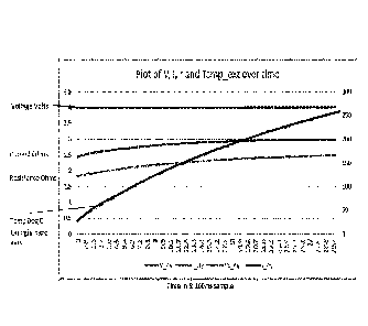
Figure 3 shows an example of measured values of Vs, Is, r and T shown on the
y-axis against time t of operation of the resonant circuit 150 on the x-axis.
It can be seen
that at an essentially constant DC supply voltage V, of around 4V, over a time
t of
approximately 30 seconds, the DC current Is increases from around 2.5A to
around 3A,
and the parameter r increases from around 1.7-1.812 to around 2.512. At the
same time,
the temperature T increases from around 20-25 C to around 250-260 C.
Figure 4 shows a calibration graph based on the values of r and T shown in
Figure 3 and described above. In Figure 4, temperature T of the susceptor
arrangement
110 is shown on the y-axis while the parameter r is shown on the x-axis. In
the example
of Figure 4 a function has been fitted to the plot of T against r, which in
this example is
a third-order polynomial function. The function is fitted to the values of r
that
correspond to a change in temperature T. As mentioned above, the value of the
parameter r may also change between an unloaded state (when no susceptor
arrangement 110 is present) and a loaded state (when a susceptor arrangement
110 is
present), although this is not shown in Figure 4. Thus, the range of r chosen
to be plotted
for such a calibration may be selected so as to exclude any change in r due to
changes
in the circuit, e.g. changing to/from "loaded" and "unloaded" states. In other
examples,
other functions may be fit to the plot or an array of values for r and T may
be stored in
a look-up format, for example in a look-up table. Although as mentioned above
that in
a loaded state we may not consider that r is small, it has been found that the
approximation of Equation 4a still enables an accurate track of the
temperature. Without
wishing to be bound by theory, it is thought that changes in the various
electrical and
magnetic parameters of the circuit are 'wrapped up' in the value of L of
Equation 4a.
In use, the temperature determiner 106 receives values of the DC voltage Võ
the DC current Is and the frequency fo and determines a value of the parameter
r in
accordance with Equation 5 above. The temperature determiner determines a
value for
the temperature of the susceptor arrangement 110 using the calculated value of
the
parameter r, for example, by calculating the temperature using a function such
as the
CA 03110943 2021-02-26
WO 2020/043900 PCT/EP2019/073259
32
one illustrated in Figure 4, or perfolining a look up in a table of values for
the parameter
r and temperature T obtained by calibration as explained above.
In some examples, this may allow the control circuitry 106 to take an action
based on a determined temperature of the susceptor 110. For example, the
voltage
supply may be switched off or lowered (either through lowering the voltage
supplied or
by lowering the average voltage supplied by altering a duty cycle if using a
pulse width
modulation scheme) if the determined susceptor temperature T is above a
predetermined value.
In some examples, the method of determining temperature T from the parameter
r may comprise assuming a relation between T and r, determining a change of r,
and
from the change of r determining a change in the temperature T.
Figure 4 represents a single calibration curve which is representative of a
certain
susceptor arrangement 110 geometry, material type, and/or relative positioning
to the
inductive element 158. In some implementations, particularly for
implementations
where a broadly similar susceptor arrangement 110 is to be used in a device
100, a
single calibration curve may be sufficient to account for e.g., manufacturing
tolerances.
In other words, the error in the temperature measurement (from the determined
value
of r) may be acceptable to account for various manufacturing tolerances of a
single
susceptor arrangement 110. Therefore, the control circuitry 106 is configured
to
perform the operations of determining a value of r followed by determining a
value of
the temperature T (e.g., using the polynomial curve or look-up table as
above).
In other examples, and particularly those where a susceptor has a different
shape
and/or is formed of a different material, different calibration curves (e.g.,
different third
order polynomials) may be required for these different susceptor arrangements
110.
Figure 5 shows a basic representation of a set of three calibration curves,
each of which
have an associated polynomial function (not shown) fitted thereto. As with
Figure 4,
temperature T of the susceptor arrangement 110 is shown on the y-axis while
the
effective grouped resistance r is shown on the x-axis. Purely by way of
example and for
CA 03110943 2021-02-26
WO 2020/043900 PCT/EP2019/073259
33
illustrative purposes only, curve A may be representative of a stainless steel
susceptor,
curve B may be representative of an iron susceptor, and curve C may be
representative
of an aluminium susceptor.
In aerosol generation devices 100 in which different susceptor arrangements
110
can be received and heated, the control circuity 106 may further be configured
to
determine which of the calibration curves (e.g., to select from curves A, B or
C of Figure
5) is the correct curve to use for the inserted susceptor arrangement 110. In
one example,
the aerosol generation device 100 may be fitted with a temperature sensor (not
shown)
configured to measure a temperature associated with the device 100. In one
implementation, the temperature sensor may be configured to detect the
temperature of
the environment surrounding the device 100 (i.e., the ambient temperature).
This
temperature may be representative of the temperature of the susceptor
arrangement 110
immediately prior to insertion into the device 110, assuming that the
susceptor
arrangement is not warmed by any other means other than the immediate
environment
prior to insertion. In other examples, the temperature sensor may be
configured to
measure the temperature of a chamber configured to receive the consumable 120.
As broadly shown by Figure 5, a value of r can be determined (rdet) based on
Equation (5). rdet is measured either as soon as the susceptor arrangement 110
is placed
within the device 100 (if the inductive element 158 is currently active) or as
soon as the
inductive element 158 is activated (i.e., as soon as a current begins flowing
in the circuit
150). That is, rdet is preferably determined in the absence of any additional
heating
caused by energy transfer from the inductive element 158. As seen from Figure
5, for a
given rdet there are a plurality of possible temperatures (Ti, T2, and T3)
each
corresponding to a point on one of the calibration curves. In order to
distinguish which
of the calibration curves is the most appropriate to use for the susceptor
arrangement
110 that is currently inserted into the device 100, the control circuitry 106
is configured
to firstly determine a value of r (as described above). The control circuitry
106 is
configured to obtain / receive a temperature measurement (or an indication of
a
temperature measurement) from the temperature sensor, and compare the
temperature
measurement with the temperature values corresponding to a determined r value
for
CA 03110943 2021-02-26
WO 2020/043900 PCT/EP2019/073259
34
each of (or a subset of) the calibration curves. By way of example, and with
reference
to Figure 5, if the temperature sensor senses a temperature t equal to Ti,
then the control
circuitry compares the sensed temperature T to the three temperature values
Ti, T2, T3
corresponding to the determined r value for each calibration curve A, B, and
C.
Depending on the result of the comparison, the control circuitry sets the
calibration
curve having the temperature value closest to the measured / sensed
temperature value
as the calibration curve for that susceptor arrangement 110. In the above
example,
calibration curve A is set by the control circuitry 106 as the calibration
curve for the
inserted susceptor 110. Thereafter, each time a value of r is determined by
the control
circuitry 106, the temperature of the susceptor arrangement 110 is calculated
based on
the selected calibration curve (curve A). While it has been described above
that the
calibration curve is selected/set, it should be appreciated that this can mean
either that
the polynomial equation representing the curve is selected, or the set of
calibration
values corresponding to the curve, for example in a look-up table, may be
selected.
In this regard, the comparison step described above may be implemented
according to any suitable comparison algorithm. For example, suppose the
sensed
temperature t is between Ti and T2. The control circuitry 106 may select
either of curve
A or curve B depending on the algorithm used. The algorithm may select the
curve
having the smallest difference (that is, whichever of T2-t or t-T1 is
smallest). Other
algorithms, such as selecting the greatest value (in this case T2), may be
implemented.
The principles of the present disclosure are not limited to a particular
algorithm in this
regard.
In addition, the control circuitry 106 may be configured to repeat the process
for determining the calibration curve in certain conditions. For example, each
time the
device is powered up, the control circuitry 106 may be configured to repeat
the process
of identifying the appropriate curve at the appropriate time (for instance
when the
inductive element 158 is first supplied with current). In this regard, the
device 100 may
have several modes of operation, such as an initial power on state, where
power from
the battery is supplied to the control circuitry 106 (but not to the resonant
circuit 150).
This state may be transition to through a user pushing a button on the surface
of the
CA 03110943 2021-02-26
WO 2020/043900 PCT/EP2019/073259
device 100 for example. The device 100 may also have an aerosol generating
mode
where power is additionally supplied to the resonant circuit 150. This may be
activated
either through a button or a puff sensor (as described above). Hence, the
control
circuitry 106 may be configured to repeat the process for selecting the
appropriate
5 calibration curve when the aerosol generating mode is first selected.
Alternatively, the
control circuitry 106 may be configured to determine when a susceptor
arrangement is
removed (or inserted into) the device 100, and is configured to repeat the
process for
determining the calibration curve at the next appropriate opportunity.
10 While it has been described above that the control circuitry makes use
of
Equations 4a and 5, it should be appreciated that other equations achieving
the same or
similar effect may be used in accordance with the principles of the present
disclosure.
In one example, Rdyn can be calculated based on the AC values of the current
and
voltage in the circuit 150. For example, the voltage at node A can be measured
and, it
15 has been found that this is different from V, ¨ we call this voltage
VAC. VAC can be
measured practically by any suitable means, but is the AC voltage within the
parallel
LC loop. Using this, one can determine an AC current, 'AC, by equating the AC
and DC
power. That is, VAcIAc=VsIs. The parameters V, and L can be substituted with
their AC
equivalents in Equation 5, or any other suitable equation for the parameter r.
It should
20 be appreciated that a different set of calibration curves may be
realised in this case.
While the above description has described the operation of the temperature
measurement concept in the context of the circuit 150 which is configured to
self-drive
at the resonant frequency, the above described concepts are also applicable to
an
25 induction heating circuit which is not configured to be driven at the
resonant frequency.
For example, the above described method of determining the temperature of a
susceptor
may be employed with an induction heating circuit which is driven at a
predetermined
frequency, which may not be the resonant frequency of the circuit. In one such
example,
the induction heating circuit may be driven via an H-Bridge, comprising a
switching
30 mechanism such as a plurality of MOSFETs. The H-Bridge may be
controlled, via a
microcontroller or the like to use a DC voltage to supply an alternating
current to the
inductor coil at a switching frequency of the H-Bridge, set by the
microcontroller. In
CA 03110943 2021-02-26
WO 2020/043900 PCT/EP2019/073259
36
such an example, the above relations set out in equations (1) to (5) are
assumed to hold
and provide a valid, e.g. usable, estimate of the temperature T for
frequencies in a range
of frequencies including the resonant frequency. In an example, the above
described
method may be used to obtain a calibration between the parameter r and the
temperature
T at the resonant frequency and the same calibration then used to relate r and
T when
the circuit is not driven at resonance. However, it should be appreciated that
the
derivation of Equation 5 assumes that the circuit 150 operates at a resonant
frequency
fo. Therefore, it is likely that the error associated with the determined
temperature
increases with an increasing difference between the resonant frequency fo and
the pre-
determined drive frequency. In other words, a temperature measurement with a
greater
accuracy can be determined when the circuit is driven at, or close to, the
resonant
frequency. For example, the above method of relating and determining r and T
may be
used for frequencies within a range fo ¨ Af to fo + Af, where Af may, for
example, be
determined experimentally by measuring the temperature of the susceptor T
directly
and testing the above derived relationships. For example, larger values of Af
may
provide lower accuracy in the determination of the temperature T of the
susceptor, but
may still be usable.
In some examples, the method may comprise assigning Vs and L constant values
and assuming that these values do not change in calculating the parameter r.
The voltage
Vs and the current L may then need not be measured in order to estimate the
temperature
of the susceptor. For example, the voltage and current may be approximately
known
from the properties of the power source and the circuit and may be assumed to
be
constant over the range of temperatures used. In such examples, the
temperature T may
then be estimated by measuring only the frequency at which the circuit is
operating,
and using assumed or previously measured values for the voltage and current.
The
invention thus may provide for a method of determining the temperature of the
susceptor by measuring the frequency of operation of the circuit. In some
implementations, the invention thus may provide for a method of determining
the
temperature of the susceptor by only measuring the frequency of operation of
the
circuit.
CA 03110943 2021-02-26
WO 2020/043900 PCT/EP2019/073259
37
The above examples are to be understood as illustrative examples of the
invention. It is to be understood that any feature described in relation to
any one
example may be used alone, or in combination with other features described,
and may
also be used in combination with one or more features of any other of the
examples, or
any combination of any other of the other examples. Furthermore, equivalents
and
modifications not described above may also be employed without departing from
the
scope of the invention, which is defined in the accompanying claims.