Note: Descriptions are shown in the official language in which they were submitted.
CA 03113260 2021-03-17
WO 2020/068711
PCT/US2019/052541
THICKNESS MEASUREMENT WITH INDUCTIVE
AND OPTICAL DISPLACEMENT SENSORS
FIELD
[0001] Disclosed embodiments relate to measuring the thickness of a coating
on a
metal foil.
BACKGROUND
[0002] Eddy currents, also called Foucault currents, are loops of
electrical current
induced within an electrical conductor by a time-varying magnetic field. A
current flowing
in a conductor, such as flowing in a wire of a coil, generates a magnetic
field, while a time-
varying current generates a time-varying magnetic field (referred to as an
originating
magnetic field for eddy current sensing) which induces an eddy current flowing
within an
electrically conductive sheet (conductor), where the resulting eddy currents
in the conductor
oppose those of the originating magnetic field. Pulsed eddy currents are used
for measuring
the thickness of an electrically conductive layer, as well as the thickness of
a coated substrate
comprising an electrically conductive coating layer on an electrically
conductive substrate.
[0003] Lithium-ion batteries utilize coated substrates for the anode
and cathode
electrodes. The process of manufacturing lithium-ion batteries generally
begins by mixing an
electrochemical slurry comprising a graphite compound for the anode and a
lithium-metal-
oxide compound for the cathode which acts as electron collector during the ion
flow within
the battery cell. This slurry is then spread evenly onto metallic foils to
form the electrodes,
commonly through a process generally called slot die coating. The substrate
for the
electrodes in lithium-ion batteries generally comprise copper foil (for the
anode) and
aluminum foil (for the cathode). After the metal substrate has been evenly
coated with the
slurry, the coated substrate is put into an oven to dry the slurry. Once the
anode and cathode
have been dried to form electrodes, each electrode is compressed to a desired
thickness
between calender rolls. To form a battery, a separator is placed between the
anode and
cathode inside a metal container, electrolyte is added, and the electrodes are
electrically
connected to leads.
SUMMARY
[0004] This Summary is provided to introduce a brief selection of
disclosed concepts
in a simplified form that are further described below in the Detailed
Description including the
drawings provided. This Summary is not intended to limit the claimed subject
matter's scope.
1
CA 03113260 2021-03-17
WO 2020/068711
PCT/US2019/052541
100051 Disclosed embodiments recognize known pulsed eddy current
methods for
measuring the thickness of a coated substrate comprising an electrically
conductive coating
layer on an electrically conducting substrate (e.g., an electrode coating on
at least one side of
a metal foil for the electrodes for lithium ion battery applications) have
problems including
complicated calibrations, lack of needed accuracy, and slow measurements due
to the
complicated calculations involved. Furthermore, known pulsed eddy current
methods
generally require that the electrode to be in physical contact with the coil.
To measure the
coating thickness, the coating side is generally positioned up against the
coil, thus being held
in physical contact with the measurement coil, or alternatively to being
physically contacted
being at a known, the electrode can be at a fixed distance from the coil.
[0006] One disclosed embodiment comprises a sensor system comprising
an eddy
current sensor (also known in the art as an inductive z-sensor) including at
least one coil with
excitation electronics coupled across the coil. An optical displacement sensor
is on top of
(above) and is concentric with the eddy current sensor so that a vertical
distance between the
eddy current sensor and optical displacement sensor is a fixed distance. The
vertical distance
between the sensors can be known, or can be determined during a sensor system
calibration.
A computing device including a processor with an associated memory is coupled
to receive
sensor data from the eddy current sensor and from the optical displacement
sensor. The
computing device is for measuring a coated substrate comprising a coating
layer on at least
one side of a metal substrate by analyzing sensor data to determine at least a
thickness of the
coating layer.
BRIEF DESCRIPTION OF THE DRAWINGS
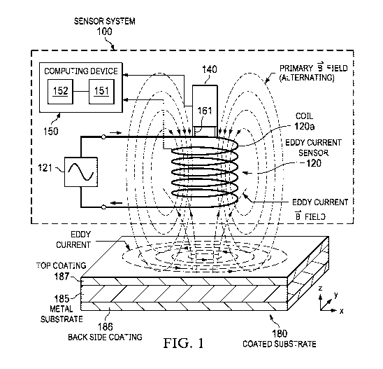
[0007] FIG. 1 shows an enhanced perspective top view depiction of a
disclosed
sensor system for measuring the thickness of a coated substrate comprising an
electrically
conductive coating layer (e.g., an electrode coating) on an electrically
conducting substrate
(e.g., metal foil), where the sensor system includes an optical displacement
sensor and an
eddy current sensor.
[0008] FIG. 2A shows a top perspective view of an example sensor
system for
measuring the thickness of a coated substrate that further comprises a scanner
shown as a C-
frame including a translation mechanism, where the eddy current sensor and the
optical
displacement sensor are contained within the scanner.
[0009] FIG. 2B shows a more detailed view of a scanner showing a top
head and a
bottom head, and a translation mechanism shown as a translation stage
configured for
2
CA 03113260 2021-03-17
WO 2020/068711
PCT/US2019/052541
scanning the C-frame. In this arrangement both the top head and the bottom
head include an
optical displacement sensor and an eddy current sensor.
[00010] FIG. 3 depicts a coated substrate having coatings on both
sides of a metal foil,
with distances to sensors above and below the coated substrate shown.
[00011] FIG. 4A shows a plot of impedance versus z-range for different
coating
thicknesses.
[00012] FIG. 4B shows a plot of Pa versus the coating thickness, where
Pa is a number
representing the first term of a polynomial.
[00013] FIG. 5 shows the relative phase angle of an impedance at a 100
kHz (in
degrees) vs. the range (distance) to an electrode coating (in mm) that is on a
metal foil
substrate using the sensor system shown in FIG. 1.
[00014] FIG. 6 shows the magnitude of impedance (in Ohms) at 100 kHz
as a function
of the range (distance) from the top of the electrode coating for the
measurement system
shown in FIG. 1.
1000151 FIG. 7 shows the impedance at 100 kHz for a single foil with
differing
amounts of cathode coating material using the measurement system shown in FIG.
1.
[00016] FIG. 8 shows an example of a calibration for an anode coating
material that
plots impedance versus range to the electrode (in mm).
DETAILED DESCRIPTION
[00017] Disclosed embodiments are described with reference to the attached
figures,
wherein like reference numerals are used throughout the figures to designate
similar or
equivalent elements. The figures are not drawn to scale and they are provided
merely to
illustrate certain disclosed aspects. Several disclosed aspects are described
below with
reference to example applications for illustration. It should be understood
that numerous
specific details, relationships, and methods are set forth to provide a full
understanding of the
disclosed embodiments.
[00018] FIG. 1 shows an enhanced perspective top view depiction of a
disclosed
sensor system 100 for measuring the thickness of an electrically conductive
coating layer
(e.g., an electrode coating) on an electrically conducting substrate, where
the sensor system
100 includes at least one optical displacement sensor 140 and at least one
eddy current sensor
120 comprising at least one coil 120a. The optical displacement sensor 140 is
located on top
of and concentric with the coil 120a so that a measurement axis of the optical
displacement
sensor 140 is collinear with an axis of symmetry of the coil 120a. A coated
substrate 180 is
3
CA 03113260 2021-03-17
WO 2020/068711
PCT/US2019/052541
shown comprising a metal substrate generally comprising a metal foil 185 that
has a coating
thereon on at least one side shown as a top coating 187 and a back side
coating 186.
[00019] The optical displacement sensor 140 is on top of and
concentric with the coil
120a. By concentric it is meant that the measurement axis of the optical
displacement sensor
140 is collinear with the axis of symmetry of the coil 120a. In some cases,
the coil may not
be circular shaped as shown in FIG. 1, such as being shaped oval or some other
shape. If the
coil 120a is shaped oval, the eddy current measurement will have better
spatial resolution in
the shorter axis dimension). The eddy current sensor 120 can be configured
with a single coil
120a as shown in FIG. 1, or the eddy current sensor can be realized with two
coils comprising
a separate excitation coil that receives the excitation signal and a so-called
pickup coil that
receives the magnetic field generated by the eddy current induced to flow in
the coated
substrate 180.
[00020] There is an attachment structure 161 for fixing (holding
constant) the vertical
(z-axis) distance between a reference plane of the optical displacement sensor
140 and a
reference plane of the coil 120a of the eddy current sensor 120. The coil 120a
is physically
attached to attachment structure, typically as known in the art being wound
around a coil
form which provides the coil 120a mechanical stability. The coil form
generally comprises a
dielectric material (typically a ceramic) form to have a hollow center. In
practice the coil
form extends vertically beyond the coil (including above the coil 120a) and
can have threaded
.. screw holes so that the optical displacement sensor 140 can be screwed into
the coil form to
be positioned at a fixed distance above the top of the coil 120a. Coil forms
are commonly
used to hold a specified number of turns of the coil on a specified diameter
former. The coil
form may or may not be used in conjunction with a coil form "tuning slug". A
tuning slug in
a coil form leads to greater inductance with fewer turns of the coil 120a.
[00021] The sensor system 100 includes excitation electronics 121 that is
shown
coupled across the coil 120a. The excitation electronics 121 generally
comprises a pulsed
current source rather than a pulsed voltage source. One generally wants the
magnetic field
generated by the coil 120a to be the same, and that can be controlled by
keeping the current
through the coil 120a the same. The voltage needed to maintain the same
current in the coil
120a will change with the arrangement of conductors near the coil 120a due to
mutual
inductance.
[00022] As noted above the coil 120a will generally be wound around a
coil form that
generally comprises a dielectric material. This coil form feature is shown
generally in FIG. 1
4
CA 03113260 2021-03-17
WO 2020/068711
PCT/US2019/052541
as an attachment structure 161. A coil form will provide mechanical stability
to the sensor
system arrangement. To enhance the dimensional stability and stability of the
electrical
properties of the coil 120a, the coil 120a may be thermally stabilized.
[00023] It may be desirable to make the coil form out of a material
such as sintered
A1203 which has good mechanical stability and good thermal conductivity while
being a good
electrical insulator. The accuracy of the eddy current measurement improves
the closer the
coil 120a can be to the electrode (-5 mm range is generally easily
achievable). Additionally,
the spatial resolution will improve the smaller the coil 120a can be. Accurate
optical
displacement sensors 140 will typically have a range of 25 to 30 mm.
Therefore, the optical
displacement sensor 140 is usually placed above the coil 120a as shown in FIG.
1. Generally,
these measurements will be co-linear as one is trying to measure the
properties of a
representative patch along this line. It is recognized that the measurement
area of the coil
120a is larger than that of the optical displacement sensor 140.
[00024] However, one is generally interested in average and
representative
measurements. Therefore, averaging is done spatially with the electrode
movement and by
using a scanner such as shown in FIG. 2A and FIG. 2B described below for
scanning the
optical displacement sensor 140 and the eddy current sensor 120 across the
coated substrate
that can comprise an electrode sheet.
[00025] The optical displacement sensor 140 that can comprise a laser
triangulation
sensor, or another type of displacement sensor, such as a chromatic confocal
displacement
sensor. The excitation electronics 121 such as a current source may be more
than a current
source, to enable it to measure the complex impedance (both the magnitude and
phase of the
impedance). Alternatively, these functions can be separated, so the excitation
electronics 121
can excite a primary coil functioning as a current source, and a separate box
having a
computing device and a secondary coil can measure the response from the coated
substrate
(e.g. electrode) electrode in a measurement equivalent to the impedance and
phase
measurement, a measurement of voltage or current, and the phase.
[00026] The sensor system 100 can accurately measure the thickness of
an electrode
coating on at least one side of a metal substrate 185, enabled by the eddy
current sensor 120,
operated-for accurately measuring the z-position of the metal substrate
(typically a 9 to 20 i.tm
thick foil), where the coated substrate can be for a lithium-ion battery
having an anode or
cathode coating on a metal substrate 185 . The electrode coating is typically
about 75 i.tm
thick, but can be up to 250 i.tm thick. The eddy current sensor 120 can
optionally be operated
5
CA 03113260 2021-03-17
WO 2020/068711
PCT/US2019/052541
as a pulsed sensor by the excitation electronics 121 configured to provide a
suitable pulse
signal.
[00027] In the production of lithium ion batteries, composite
electrodes are first
manufactured. As described in the background above, these electrodes are
generally made by
coating a metal foil substrate (usually aluminum or copper) with a coating.
For example, the
anode can comprise primarily graphite and the cathode can comprise a lithium
metal oxide
(e.g. LiCo02). Each of these electrode materials may have binders and
conductivity
enhancers added. A slurry is made of all the components which is then applied
to the foil on
one side or on both sides of the foil. The coating can then be dried and
calendered.
Producers of battery electrodes are interested in knowing the thickness of the
anode or
cathode coating in order to control this thickness. Additionally, producers of
lithium battery
electrodes may be interested in knowing not just the total electrode coating
thickness of a
double-sided coated metal substrate, but also the thickness of each of the
sides of the
electrode coating.
[00028] One way to measure the thickness of a coating on a metal substrate
is to use
the optical displacement sensor 140 shown in FIG. 1, collocated with an eddy
current sensor
120 comprising at least one coil 120a. However, eddy current sensors normally
operate at
frequencies of or less than 1 MHz where the measurement skin depth is greater
than 50 i.tm,
but the thickness of the metal substrate when comprising a metal foil for a
lithium battery is
as noted above is generally less than 20 i.tm thick. When the skin depth is
greater than the
thickness of the metal foil the thickness measurements can be greatly affected
by small
variations in the metal foil thickness. In a test calculation of 17- i.tm
thick copper foil
measured with an eddy current sensor with a 40-mm-diameter coil at a measuring
range of 13
mm, it was found that even a 1% variation of copper foil thickness leads to
>10 i.tm changes
in measured range leading to a >10 i.tm change in the calculated electrode
coating thickness.
This electrode coating thickness measurement error is large enough to likely
be unacceptable
to battery electrode producers. Disclosed aspects solve this problem by not
assuming that the
coating is non-electrically conducting, but instead by also taking the
conductivity of the
coating into account while calculating the distances to the metal substrate
(foil) and to the
surface of the coating (the electrode surface).
[00029] Aside from a measurement of caliper (thickness) for the
electrode coating on a
metal substrate, battery producers may also be interested in determining other
product
qualities such as the electrical conductivity of the electrode coating. An
integrated electrical
conductivity and thickness measurement is believed to be not currently
available, which the
6
CA 03113260 2021-03-17
WO 2020/068711
PCT/US2019/052541
sensor system 100 provides. The most commonly used known measurement
techniques
cannot measure a coating on each side of a metal foil individually.
[00030] As described above, the sensor system 100 is based on an
optical displacement
sensor 140 above a coil 120a of an outer positioned eddy current sensor 120
which are
attached (typically using a coil form) to each other so that the distance
along the z-axis (the
vertical offset) between them is fixed. The range to the top surface of the
coated substrate
(electrode) can be measured by the optical displacement sensor 140, that is
the range from a
reference plane of the optical displacement sensor 140. Calibrations will be
done with this
arrangement and the sensor devices should not move with respect to each other
for the
calibrations to remain valid. The eddy current sensor provides a measurement
which is a
function of the thicknesses, electrical conductivities, and range to the
electrode coating(s) 187
and 186, and the metal substrate 185, which as noted above can be a metal
foil.
[00031] The optical displacement sensor 140 can comprise a diode-laser
triangulation
sensor. However, it is also possible to use other optical displacement sensor
types. The
optical displacement sensor 140, such as the triangulation device, is able to
accurately
measure the range (vertical distance) to the top surface of the electrode
coating shown in FIG.
1 as the top coating 187. Commercial optical displacement sensor products are
available
which can make this range measurement to an accuracy of less than 1 m
(typically a 0.5 pm
2 standard deviation (2c7)).
[00032] In one embodiment, a conventional eddy current sensor is used in
which a
single frequency from the excitation electronics 121 is used to excite a coil
120a that can
comprise a multi-turn coil, and the response of the coated substrate 180 is
monitored either on
the same coil 120a used for the excitation or on a nearly coincident secondary
coil. The
response phase and magnitude can be measured. The excitation frequency used
will
generally be in the range of 50 kHz to 1,000 kHz (1 MHz).
[00033] In another embodiment, if more information about the coated
substrate 180
than just the coating layer thickness is desired, such as the electrical
conductivity of the
coated substrate 180, a pulsed eddy current technique can be employed. A
repetitive pulsed
signal such as a square wave pulse voltage may be applied to a coil 120a of an
eddy current
sensor by excitation electronics 121 (e.g., a pulse duration of 5 to 15
seconds) and the
response of the coated substrate 180 is then measured by the coil 120a or by
another coil,
generally with an Analog-to-Digital-Converter (ADC) coupled to the coil 120a
or another
coil, where the ADC has its output coupled to a processor 151 of the computing
device 150
shown in FIG. 1.
7
CA 03113260 2021-03-17
WO 2020/068711
PCT/US2019/052541
[00034] The reception of the response function for the eddy current
sensor can be at
the primary coil that also provides the magnetic field to the electrode coated
metal foil, or at a
secondary (pickup) coil that may also be used to receive the response
function. Alternatively,
instead of applying square wave pulses, it is also possible for the excitation
electronics 121 to
apply a swept frequency to the primary coil and measuring the response as a
function of the
frequency. To obtain the coating layer thicknesses, calculations are generally
made with a
processor 151 such as a microprocessor having associated memory 152, shown as
a
computing device 150 in FIG. 1. The measured response is a function of the
range to the
electrode and the thickness and electrical conductivity of each layer (e.g.,
top coating 187 and
the metal substrate 185).
[00035] It is possible to determine a number of different parameters
from the measured
results. It is expected that because if one tries to extract all these
parameters from the sensor
data the result will have low accuracy for any individual parameter.
Therefore, a fit can be
performed within a range of expected values, and an optical displacement
sensor 140 such as
a laser triangulation device can be used to provide a range (distance) to the
top surface of the
coating layer shown as top coating 187 in FIG. 1. It is also expected that the
electrical
conductivity of the metal substrate 185 that may comprise a metal foil
material will be well-
known (e.g., the bulk electrical conductivity of copper is well known), or can
be determined
prior to disclosed thickness measurements. It should also be noted that due to
the generally
relatively thin metal foils for the metal substrate 185, the back side coating
186 may need to
be taken into account in the thickness calculations. It is also noted a main
novelty of this
disclosed aspect is the use of an optical displacement sensor 140 to determine
the range to the
electrode coating meaning that the known art generally employs a fixed
standoff whereas in
disclosed systems the coated substrate generally in the form of a sheet is
allowed to move in
the z-direction, that is the range from the eddy current sensor to the top
surface of the
electrode (the coating) that does not have to be kept constant, and one
measures its range
(standoff) with respect to the optical displacement sensor 140.
[00036] One approach to calculating the desired parameters
(specifically the coating
layer 187 and 186 thicknesses) but also the electrical conductivity of the
coated substrate 180,
is to fit the measured waveform to the expected results using a least-squares
method.
However, instead of doing a detailed comparison to theory, most of the needed
information
can generally be obtained by simple waveform measurements (e.g., peak, peak
timing, and
zero crossing time) which can be compared to a three-dimensional look-up table
based on
theoretical calculations. This can significantly speed up the thickness
calculation times.
8
CA 03113260 2021-03-17
WO 2020/068711
PCT/US2019/052541
[00037] What is generally important for making an accurate thickness
measurement for
coating layers including for at least a top coating 187 on a metal substrate
185 is generally
that there be a significant difference in the electrical conductivities
between the metal
substrate 185 that generally comprises foil and the coating, such as the top
coating 187. This
should not be a difficulty as metal foil substrates generally have very high
relative electrical
conductivities and the electrode coatings generally do not have electrical
conductivities much
greater than graphite. It is therefore likely that there is generally at least
a 500 times
difference in these electrical conductivities. In the limit of low electrode
coating layer
electrical conductivity, the eddy current measurement would thus essentially
be that of the
underlying metal foil and the measurement would be a combination of the
optical
displacement sensor 140 measurement to the top surface of the top coating 187
and an
inductive measurement from the eddy current sensor 120 to the top surface of
the metal
substrate 185 that as described above generally comprises a metal foil.
[00038] As described above, the eddy current sensor 120 is generally
mechanically
coupled to the optical displacement sensor 140 by the attachment structure
161, and the
projected laser beam from the optical displacement sensor 140 is concentric
with the coil
120a of the eddy current sensor 120. It is generally important that the height
(z-axis) offset
between the coil 120a of the eddy current sensor 120 and the optical
displacement sensor 140
be fixed. To ensure this, the coil 120a of eddy current sensor 120 and the
optical
displacement sensor 140 are normally mechanically attached to each other by
the attachment
structure 161, and they may each even be temperature controlled. A i.tm of z-
axis movement
between the coil 120a of the eddy current sensor 120 and the optical
displacement sensor 140
will generally lead to a i.tm range measurement error.
[00039] As noted above, the optical displacement sensor 140 measures
the range to the
top of the top coating electrode coating, and the inductive sensor indirectly
measures
((calculated) ideally to the top of the metal substrate 185 generally
comprising a metal foil.
To measure to the top of the metal substrate 185 such as a metal foil, one
generally needs to
know the thickness of the metal substrate 185. However, because the electrode
coating
material is also electrically conductive, the eddy current sensor
measurements¨should
generally take the electrical conductivity of the coating into account to
enable being able to
produce accurate readings of the electrode coating thickness. The sensor
system 100 and
method using this sensor system can make accurate (typically ¨1 pm)
measurements of the
thickness of an electrically conductive coating on a metal substrate 185
comprising a thin
metallic foil.
9
CA 03113260 2021-03-17
WO 2020/068711
PCT/US2019/052541
[00040]
Disclosed sensor systems overcome the above-described problems when
measuring the thickness of an electrically conductive coating on an
electrically conducting
substrate (such as electrode for a lithium-ion battery) by providing improved
measurement
accuracy and speed by rather than needing complicated multi-component curve
fitting for
every measurement, disclosed methods instead utilize relatively simple
calculations, while
generally enabling off-the-shelf hardware including respective Eddy current
and optical
displacement sensors and power supplies can be used.
[00041]
FIG. 2A shows a top perspective view of an example sensor system 200 for
measuring the thickness of a coated substrate that further comprises a scanner
190 shown as a
C-frame including a translation mechanism (see the translation mechanism 195
in FIG. 2B
described below), where the coil 120a of the eddy current sensor and the
optical displacement
sensor 140 are contained within a head shown as a top head 191 of the scanner
190.
[00042]
FIG. 2B shows a more detailed view of a scanner 190 in the sensor system 200
showing a top head 191 and a bottom head 192, and a translation mechanism 195
shown as a
translation stage configured for scanning the C-frame 198. There are known
different ways
of moving the C-frame 198 besides what is commonly known as a translation
stage. In this
arrangement both the top head 191 and the bottom head 192 both include an
optical
displacement sensor and an eddy current sensor shown as optical displacement
sensor 140a
and coil 120a in the top head 191 and optical displacement sensor 140b and
coil 120b in the
bottom head 192. The coil 120a of the eddy current sensor in the top head 191
and the coil
120b of the eddy current sensor in the bottom head 192 are generally operated
at different
frequencies to avoid interference between the two eddy current sensors.
[00043]
It is now described how to use a disclosed system with a scanner such as the
scanner 190 shown in FIG. 2A and 2B. Sheet material producers, such as lithium
battery
producers, will generally always want to know the total caliper (thickness) of
the product.
And a double-sided optical measurement can produce that. One may use a
scanning C-frame
198 because it is important that the optical measurements be well aligned to
avoid error.
With a C-frame 198, the top and bottom heads 191 192 are well aligned because
they do not
move independently. The whole C-frame scans the coated substrate 180 that is
generally the
form of a sheet as it is mounted on a translation mechanism 195 such as a
translation stage.
[00044]
One generally needs to know the distance between the top head 191 and the
bottom head 192. This can be done with a mechanical design and periodic
standardization
CA 03113260 2021-03-17
WO 2020/068711
PCT/US2019/052541
against a known-thickness reference tile, or it can be measured (if one has a
less-stiff frame)
with a magnetic z-sensor such as Hall-effect, giant-magnetoresistance (GMR),
or fluxgate
sensor, also with periodic standardization.
[00045] FIG. 3 depicts a coated substrate 180 having coatings on both
sides of a metal
foil 185' shown as a top coating 187 and a bottom coating 186, with distances
to the sensors
above and below the coated substrate 180 shown along with an equation (the
total thickness
(Ztot) of the coated substrate 180 being equal to Ztot ¨ 01 -02) for
calculating the coating
thicknesses. As described below, one can thus obtain the top coating 187
thickness and the
metal foil 185' thickness from the eddy current sensor shown as the coil 120a
combined with
the 01 distance calculated by the optical displacement sensor 140a.
[00046] For example, a C-frame can be provided such as shown in FIG.
2A and FIG.
2B as 198 which has dimensions not changed by more than about 0.1 i.tm as it
scans the
coated substrate (sheet). However, the dimensions of the C-frame may change
with
temperature. Therefore, periodically, for example every 20 minutes, one can
use the sensor
system to measure known thickness tk, where Ztot = tk + 01 + 02. By utilizing
a sensor that
can measure through the coated substrate, such as a Hall effect, GMR, or
fluxgate sensor that
is magnetically based that provides a coil in both a top head and in a bottom
head of a
scanner. If one knows the total thickness, and the thicknesses of the foil and
the coating on
one side then one can calculate the thickness of the coating on the other
side. Alternatively,
one can have two eddy current sensors and directly measure the thicknesses of
the coatings
on each side.
[00047] FIG. 4A shows a plot of impedance versus z-range for different
coating
thicknesses. The impedance values are provided by the eddy current sensor, and
the z-range
is provided by the optical displacement sensor 140. Curves are shown for
different
thicknesses of the foil shown as ti, t2 and t3. As described below the terms
Pi, P2 and P3 are
polynomials. Pi as used herein is PIA, P113, Plc and then the Impedance =
Pi(z) = PIA Z2 + P1B
Z + Pic when the full expression for the polynomial is written out.
[00048] FIG. 4B shows a plot of PA versus coating thickness showing
data points at ti,
t2 and t3. As noted above, PA is the first term in a polynomial, and there
could be constructed
similar curves for PB and Pc.
11
CA 03113260 2021-03-17
WO 2020/068711
PCT/US2019/052541
[00049] Below is described a single frequency method of using a
disclosed sensor
system comprising eddy current sensor 120 comprising at least one coil 120a
and an optical
displacement sensor 140 to measure the thickness of an electrically conductive
coating layer
shown as top coating 187 in FIG. 1 on a metal substrate 185 that can comprise
an electrically
conductive foil substrate. The eddy current sensor 120 measurement performed
is made
somewhat complex by generally needing to take into account the magnitude of
the impedance
as well as its phase. While it is possible to use only the magnitude if the
thickness of the
metal foil is constant, one generally needs to use the phase information to
determine the metal
foil's thickness.
[00050] To make a measurement using the sensor system 100, one generally
first
calibrates the respective eddy current sensor 120 and optical displacement
sensor 140. For
the optical displacement sensor 140, one can either use the manufacturer's
calibration, or
calibrate against a target at a known range such as calibrating against a
target translated
through the measurement range. The reference measurement can be provided by an
interferometer or an optical encoder. The eddy current sensor calibration is a
bit more
difficult as the measurement of magnitude and phase of the impedance depends
on not just
the range to the measurement target (here the top coating 187 of the coated
substrate 180),
but also on the thickness of the relatively high electrical-conductivity metal
substrate 185 that
can comprise a metal foil.
[00051] The calibration can first be performed with the metal foil that for
lithium
battery applications can be used as the electrode current collector. That is,
the coated
substrate 180 sample can be placed parallel to the coil 120a of the eddy
current sensor 120
and moved up and down throughout the measurement range while the coil 120a
impedance
(magnitude and phase) and range is recorded. The range (to the top of the top
coating 187)
can be measured with the optical displacement sensor 140, or another sensor
such as a linear
variable differential transformer (LVDT) which is also called linear variable
displacement
transformer mechanically in contact with the back surface of the electrode,
can be used. If
the optical displacement sensor 140 is used, it may be helpful to place a
diffusely scattering
material (such as pigmented and calendered vinyl) of known thickness on the
otherwise
secularly reflecting surface of the metal foil to obtain accurate range
measurements.
[00052] The measurements are then generally repeated with a second and
third layer of
metal foil. Alternatively, if finer gradations of metal foil of the correct
composition are
available, they should generally be used. At this stage, the most important
information is
12
CA 03113260 2021-03-17
WO 2020/068711
PCT/US2019/052541
shown in FIG. 5 which shows the phase angle (in degrees) as a function of
range to the top
coating 187 and the metal foil thickness.
[00053] It can be seen that this relationship is essentially entirely
dependent on the
thickness of metal foil substrate present rather than the thickness of the
electrode coating. In
this case, the metal foil/current collector comprised 10- i.tm thick copper.
The measurement
was made with an HP4277 LCZ meter that is a commercially available impedance
measuring
instrument and an MTI Instruments Microtrack 3 laser triangulation device as
the optical
displacement sensor 140. Since coated substrate samples with multiple
thicknesses of the
metal foil were not available, the effect by using an electrode sample and
placing layers of
foil of the same thickness behind it were simulated.
[00054] From the phase vs range data, one can make measurements of the
range to the
electrode (top coating) and phase angle to determine the foil thickness. A
simple way to do
this is to construct a polynomial which represents the phase as a function of
the range. First a
polynomial is fit to each phase vs range curve (for instance three curves if
there are three
different foil thicknesses and if it is a second order polynomial then there
will be three
components for each curve. In this case thickness 1 will be represented by a
polynomial Pi,
thickness 2 by P2 etc. Each polynomial will have three terms as they are
second order
polynomials: P1=P1Az2+P1Bz+P1c. One can then construct a polynomial for an
arbitrary
thickness. One can do this by fitting a line or a curve to each of the terms
in the polynomial.
to illustrate this with a polynomial curve see fig. 4B described below.
[00055] PA is thus the first term in the polynomial for an arbitrary
thickness, t. One
can put three points on this graph, PA1, PA2, and PA3 on the y axis and the
corresponding
thicknesses on the x axis. One can make corresponding curves for PB and Pc.
With this
information, one can draw a phase vs range curve for any thickness (t). This
is important
because if one makes a measurement of range and phase, this will define a
point on the 2D
graph and one can then solve this family of equations to give a unique t which
is the
measured foil (metal substrate) thickness. It is noted in this above
description is presented as
phase vs. range where the y axis is labeled impedance vs. range, where the
process is the
same, just the label on the graph is different.
[00056] In a similar way, Impedance vs range to the bare-foil curves can be
then
generated for arbitrary metal foil thicknesses by fitting each impedance vs
range curve to a
polynomial (a second order polynomial is generally sufficient), and then
interpolating
between them the curves as a function of metal foil thickness. This
calibration can be
13
CA 03113260 2021-03-17
WO 2020/068711
PCT/US2019/052541
performed on-machine, or it can be performed in a factory or elsewhere, and
can be stored in
a memory of a computer device such as shown in FIG. 1, or on-board.
[00057] On-machine means at a production site where the foil thickness
may change
from time to time. If performed on-machine, then some sort of arrangement for
precisely
translating the coated substrate sample through the measurement range
generally is
constructed. If the coated substrate such as an electrode to be measured is
double sided, the
calibration should be performed with a single side coated electrode with a
comparable foil
thickness. The calibration of foil thicknesses should be done with the coating
on the opposite
side of the measurement. Similarly, additional foil layers can be added on top
of the foil to
calibrate for arbitrary foil thickness. This works because the coating on the
back side of the
electrode only has a small effect on the calibration. Small variations in the
thickness of the
back side coating do not significantly change the calibration results.
[00058] Next, measurements should generally be performed to determine
the effect of
the electrode coating. In the simplest case one can perform the same
calibration procedure
that was used for the metal foil but use a coated substrate 180 sample
instead. The
description below is for electrodes for lithium ion batteries. However, the
disclosed
technique applies to other similar products, such as electrodes for other
battery types, or
electrodes for fuel cells.
[00059] The procedure for disclosed thickness measuring for anodes and
cathodes can
be essentially the same. For the cathode it was found that the impedance
measurement to the
foil surface was insensitive to the amount of cathode coating. This is just
because the
cathode conductivity is generally lower as compared to the anode coating. Some
published
values are that the anode coating may have an electrical conductivity around
105 S/m and the
cathode coating may have a lower conductivity as compared to the anode of
generally about
-1 S/m. In some cases, the cathode conductivity may be higher than 1 S/m, and
if so then the
procedure for anode thickness determination(s) can generally be used.
[00060] For the thickness measurement of a lithium-ion battery, the
measurement then
becomes relatively easy, with the optical displacement sensor 140 being used
to measure the
range to the top coating 187. The thickness of the metal substrate 185 which
generally
comprises a metal foil is calculated (if deemed needed) from the relation of
the impedance
phase to the range to the top coating 187. Then the range to the metal foil
can be determined
from the magnitude of the impedance. The thickness of the top electrode
coating is simply a
difference of these two values It is noted that if the metal foil thickness
varies, then there will
14
CA 03113260 2021-03-17
WO 2020/068711
PCT/US2019/052541
be a family of such curves and the phase measurement can be used to determine
which one to
use.
[00061] For example, one can use a second order polynomial to
represent calibrations
of the metal foil as described above. Each metal foil thickness can have its
own calibration
curve (to clarify, there is a calibration curve for phase and one for
impedance). It is relatively
simple to then to construct a relationship to calculate a polynomial for any
metal foil
thickness (see the polynomial shown in FIG. 4A and FIG. 4B described above. In
a simple
case, one can just assume the relation is linear, or one can fit a curve to
the thickness data to
more accurately predict the curve for any metal foil thickness.
[00062] If the metal foil thickness is changing, one can first measure the
thickness of
the metal foil using the impedance phase information. Just as various
thicknesses of foil
produce a family of curves on the phase vs range plot, they will also produce
a family of
curves on the impedance vs range chart. The calibration on the impedance vs
range chart can
be represented as a polynomial which is the difference between the measurement
with a
known amount of coating and the measurement of the foil only. This can be
added to a
polynomial representing an arbitrary foil thickness to get the calibration
curves for an
arbitrary thickness of anode coating on an arbitrary foil thickness. Then from
a family of
calibration curves of impedance-magnitude from the eddy current sensor (to the
laser
voltage/displacement such as from the optical displacement sensor 140) one can
compute a
polynomial which represents the response of the measurement of the metal foil.
It is noted
that this technique generally only works for cathode coating layers of low
electrical
conductivity. For cathode layers with a higher conductivity, the procedure for
the anode
coating layer described below can be used.
[00063] For the anode coating layer, the measurement is a bit more
complicated as the
.. impedance curve shifts with the coating thickness. To deal with this, one
can fit polynomials
to a metal foil curve and to a foil plus electrode coating curve. It is noted
that small
corrections may need to be applied as the foil thickness will be reduced in
the calendering
process. It is thus possible that in the process of compressing the electrode
structure, the foil
may be thinned out as well as the coating. This is generally not a significant
concern as there
.. is disclosed a procedure to deal with changes to the foil thickness as
described above. Such
fits are shown in FIG. 6 where the range to the top of the electrode coating
was measured
with a laser-based optical displacement sensor 140. The impedance was again
measured with
a HP4277 LCZ meter.
CA 03113260 2021-03-17
WO 2020/068711
PCT/US2019/052541
[00064] FIG. 7 shows the impedance measured at 100 kHz for a single
foil with
differing amounts of cathode coating material thereon using the sensor system
100 shown in
FIG. 1. The range measurement to the top surface of the electrode (to the top
surface of the
top coating 187) was performed by the optical displacement sensor 140.
However, because,
one does not know how thick the electrode coating is from the optical
displacement sensor
140, one obtains the thickness of the electrode coating using the eddy current
sensor that
enables obtaining the distance to the metal foil.
[00065] One metal foil sample was used and the electrode coating was
removed for
successive measurements. The reduced sample is the coated substrate sample
with
approximately 10 i.tm removed from the electrode coating. The surface of the
electrode (top
of the coating) was measured, but one is generally interested in the distance
to the foil. The
thickness of the coating was known. For purposes of calibration, one can
measure the
thickness with a micrometer and subtract the foil thickness which one
generally also knows
so that thickness was added to the measurement obtained from the optical
displacement
sensor 140. One generally works in terms of either the distance to the foil or
the distance to
the electrode surface. The coating thickness is the difference between the two
(electrode
surface and the metal foil).
[00066] One can construct calibration curves of impedance vs the range
for the foil and
for the coating. The more samples one has, the better the calibration curves
will be,
especially if the samples span a range covering the expected range that will
be produced on
the production line. Therefore, for the anode coating layer measurement, it is
generally
needed to locate a point on the impedance vs. range to electrode coating plot
(see FIG. 8
described below) from the coil 120a of the eddy current sensor 120 and optical
displacement
sensor 140 respectively, and then to calculate the thickness based on distance
from the
measured calibration curve.
[00067] FIG. 8 shows an example of a calibration for an anode coating
material that
plots impedance versus range to the electrode (mm). It is noted that FIG. 8
looks different
from FIG. 7 described above because FIG. 8 is for an anode and FIG. 7 is for
cathode. In
FIG. 8 dashed lines are provided showing the response of the foil shown as the
foil, and the
foil with a 76 i.tm thick electrode coating shown as being the sample, both
being shown
bolded. The bolded dashed lines for the response of the foil in the electrode
coating are a plot
of respective polynomials shown in FIG. 6 described above. There are other
dashed lines
shown depicting how 70 and 80 i.tm thick electrode calibration coatings look,
shown as 70
16
CA 03113260 2021-03-17
WO 2020/068711
PCT/US2019/052541
i.tm CAL and 80 i.tm CAL. The calibration lines are the calculated curves
based on inter-
/extrapolation of polynomial coefficients as a function of the electrode
coating thickness.
[00068]
As described above, if the metal foil thicknesses varies significantly, then
this
will also generally be corrected for. One example technique would be to assume
that the
difference caused by the electrode coating is fixed based on the electrode
coating thickness.
One could then use a baseline metal foil thickness calibration to derive a
relationship for
arbitrary metal foil thicknesses and then add the electrode coating difference
to this. The
coating thickness Pcoat= the total electrode thickness (Pelectrode) ¨ the
metal foil thickness
(Pfoil). Pfoil will vary depending on the thickness found on the phase
diagram, but can be
accounted for by making a polynomial for any foil thickness. Then one can make
a
polynomial representing this foil thickness with the coating using this
relationship. See FIG.
4B described above showing how to calculate an arbitrary polynomial given some
calibration
polynomials.
[00069]
It is noted that in the anode coating layer measurements there may be a
significant sensitivity to electrical conductivity. However, there is a cross
sensitivity between
electrical conductivity and caliper (thickness). The more the electrode
coating is calendered
the more electrically conductive will also be. If one needs to correct for
electrical
conductivity, one has the option of using this technique as described above
and estimating the
electrical conductivity based on measurements at two different frequencies.
This method can
also be extended by using a pulsed eddy current method to more accurately
determine the
thickness and the electrical conductivity of the electrode coating.
[00070]
It is also noted that the frequencies described above, 100 kHz and 1 MHz are
ones which were experimentally found to be useful for making this measurement.
Other
frequencies may be more useful if the product has different electrical
conductivities or
thicknesses than those tested. It is also possible that to get the maximum
sensitivity one may
want to measure the phase at one frequency, say 100 kHz, and the magnitude of
the
impedance at another frequency, say 1 MHz.
[00071]
Disclosed aspects can be further extended by considering disclosed
measurements are usefully employed in a scanner to determine the CD (cross
direction) and
MD (machine direction) variations in electrode coating thicknesses. These
variations can then
be used for caliper control.
[00072]
While various disclosed embodiments have been described above, it should be
understood that they have been presented by way of example only, and not
limitation.
Numerous changes to the subject matter disclosed herein can be made in
accordance with this
17
CA 03113260 2021-03-17
WO 2020/068711 PCT/US2019/052541
Disclosure without departing from the spirit or scope of this Disclosure. In
addition, while a
particular feature may have been disclosed with respect to only one of several
implementations, such feature may be combined with one or more other features
of the other
implementations as may be desired and advantageous for any given or particular
application.
18