Note: Descriptions are shown in the official language in which they were submitted.
CELLULAR MODEM FOR LOW POWER APPLICATIONS
BACKGROUND
100021 In fixed-location, battery-powered cellular applications, it is known
to provide
higher power to a cellular modem during periods of communication, and lower
power to
the cellular modem during other periods. In one example, different power
supplies are
utilized, to provide approximately 500 mA during operation of communications
functionality, and less than 10 uA during "sleep" periods. However, while
providing
different current levels to the cellular modem at different times is possible,
inefficiencies
in the design of power supplies result in a continuous current drain.
Particularly for
battery-powered devices, such current drain may be inconsistent with preferred
design
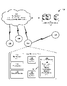
requirements.
100031 Accordingly, there is a need for a cellular modem that is better
adapted to low
power situations.
SUMMARY
10003a1 In a first aspect, there is described a cellular module, comprising: a
processor;
a memory in communication with the processor; at least one output pin having a
voltage
level controlled by the processor to: request a first power level for use by
the cellular
module during periods wherein a radio frequency (RF) communication is not
being
performed; and request a second power level for use by the cellular module
during periods
when the RF communication is being performed, wherein the second power level
is a
higher power level than the first power level; and instructions stored in the
memory, for
performing actions by execution of the processor, comprising: receiving a
signal from a
Coulomb counter, the signal having passed through one or more logic devices,
to activate
the cellular module; determining, at the cellular module, an appointed time
for a status
1
Date Recue/Date Received 2022-07-13
change of a communication; determining a time to signal one or more power
supplies,
based at least in part on the appointed time for the status change of the
communication,
so that the one or more power supplies are ready to change to supply power at
the second
power level at the appointed time for the status change of the communication;
and
changing a voltage on the at least one output pin at the determined time to
cause the one
or more power supplies to transition from the first power level to the second
power level.
[0003b] There is also described a metering device, comprising: a metrology
unit; and a
cellular module to transmit data obtained from the metrology unit, the
cellular module
comprising: a processor; a memory in communication with the processor; at
least one
output pin to: signal for a first power level for use by the cellular module
during periods
wherein radio frequency (RF) communication is not being performed; and signal
for a
second power level for use by the cellular module during periods when the RF
communication is being performed, wherein the second power level is a higher
power
level than the first power level; and instructions stored in the memory, for
performing
actions by execution of the processor, comprising: receiving a signal from a
Coulomb
counter, the signal having passed through one or more logic devices, to
activate the
cellular module; determining, at the cellular module, an appointed time for a
status change
of a communication; determining a time to signal one or more power supplies,
based at
least in part on the appointed time for the status change of the
communication, so that the
one or more power supplies are ready to change to supply power at the second
power
level at the appointed time for the status change of the communication; and
send a signal
on the at least one output pin at the determined time to cause the one or more
power
supplies to transition from the first power level to the second power level.
[0003c] There is also described a method, comprising: under control of one or
more
processors configured with executable instructions: operating a cellular
module at a first
power level, wherein the first power level is used between periods involving
radio
frequency (RF) transmission and/or RF reception, and while operating using the
first
la
Date Recue/Date Received 2022-07-13
power level: receiving a signal from a Coulomb counter, the signal having
passed through
one or more logic devices, to activate the cellular module; changing a voltage
on an output
pin to signal a transition from the first power level to a second power level,
wherein the
second power level is greater than the first power level; and operating the
cellular module
.. using the second power level, wherein operating the cellular module in the
second power
level comprises at least one of RF transmission or reception, and while
operating in the
second power level: communicating with a remote cellular radio; obtaining an
indicated
time for a communication; and signaling one or more power supplies to
transition from
the second power level to the first power level.
[0003d] There is also described a metering device, comprising: one or more
power
supplies, configured to provide power at a first power level and a second
power level; a
metrology unit, powered by the one or more power supplies; and a cellular
module,
powered by the one or more power supplies, wherein the cellular module
comprises: a
radio, configured to transmit data when powered at the second power level; a
processor,
.. to control the radio; a memory in communication with the processor; a
general-purpose
input/output (GPIO) pin, controlled by the processor, to signal the one or
more power
supplies to transition between the first power level and the second power
level, wherein
the second power level is higher than the first power level; wherein the
cellular module
performs actions comprising: receiving a signal from a Coulomb counter, the
signal
having passed through one or more logic devices, to activate the cellular
module;
receiving, at the processor and from the radio, an appointed time for a next
communication; determining a time to activate the second power level of the
one or more
power supplies, to power the radio at the appointed time for the next
communication; and
sending a signal from the GPIO pin at the determined time.
[0003e] There is also described a method of operating a cellular module,
comprising:
signaling one or more power supplies to transition between a first power level
and a
second power level, wherein the second power level is higher than the first
power level,
lb
Date Recue/Date Received 2022-07-13
and wherein the signaling is performed by voltage on a general-purpose
input/output
(GPIO) pin of the cellular module; receiving a signal from a Coulomb counter,
the signal
having passed through one or more logic devices, to activate the cellular
module;
receiving, at a processor of the cellular module and from a radio of the
cellular module,
an appointed time for a next communication; determining a time to activate the
second
power level of the one or more power supplies, to power the radio to be ready
for the next
communication at the appointed time; and sending a signal from the GPIO pin at
the
determined time.
BRIEF DESCRIPTION OF THE DRAWINGS
100041 The detailed description is described with reference to the
accompanying figures.
In the figures, the left-most digit(s) of a reference number identifies the
figure in which
the reference number first appears. The same numbers are used throughout the
drawings
to reference like features and components. Moreover, the figures are intended
to illustrate
general concepts, and not to indicate required and/or necessary elements.
lc
Date Recue/Date Received 2022-07-13
CA 03114897 2021-03-30
WO 2020/073001
PCT/US2019/054865
[0005] FIG. 1 is a block diagram showing an example system including at least
portions
of a smart natural gas or water distribution infrastructure, including gas or
water meters
that communicate within one or more cellular and/or mesh network(s), and a
computing
device.
[0006] FIG. 2 is a block diagram describing an example low-power cellular
modem
supported by a higher-current power supply (e.g., for RF transmission and/or
reception)
and a lower-current power supply (e.g., for sleep functions).
[0007] FIG. 3 is a block diagram of an example gas or water meter, showing
processor,
memory, metrology and communications devices, and showing higher-current and
lower-current power supplies controlled by logic device(s) controlled at least
in part by
a GPIO pin of a low-power cellular modem.
[0008] FIG. 4 is a block diagram of an example gas or water meter, showing
processor,
memory, metrology and communications devices, and showing a power supply
having
higher-current and lower-current modes of operation controlled by logic
device(s)
controlled at least in part by a GPIO pin of a low-power cellular modem.
[0009] FIG. 5 is a flow diagram describing example operation of a cellular
modem in
a low power application.
100101 FIG. 6 is a flow diagram describing example operation of a cellular
modem in a
low power application.
[0011] FIG. 7 is a flow diagram describing example operation of a cellular
modem,
illustrating use of a plurality of power levels for sleep and receiver and
transceiver modes
of operation.
[0012] FIG. 8 is a flow diagram describing example operation of a cellular
modem of a
device, such as in a metering device, illustrating use of a plurality of power
levels for sleep
and receiver and transceiver modes of operation.
[0013] FIG. 9 is a flow diagram describing operation of a cellular modem,
showing
example implementation and operation of additional GPIO pins.
2
CA 03114897 2021-03-30
WO 2020/073001
PCT/US2019/054865
[0014] FIG. 10 is a flow diagram describing operation of a cellular modem,
showing an
example by which power levels provided to two or more devices may be changed
in a
sequential manner.
DETAILED DESCRIPTION
Overview
[0015] The disclosure describes techniques for the structure and operation of
a cellular
modem adapted for low-power (e.g., battery-powered device) applications. The
cellular
modem is configured with software and/or operational logic (e.g., an
application specific
integrated circuit or ASIC) that controls aspects of processor(s), memory
device(s), and a
receiver, transmitter and/or transceiver for radio frequency (RF)
communication with a
cellular tower. In an RF communications mode, the transceiver exchanges
information
with the cellular tower, and receives an appointed time for a next
communication with the
cellular tower. The cellular modem then enters a low-power mode. Software or
other logic
executed by, or by a peripheral device for, the cellular modem during periods
of operation
at the low-power level may use inputs including the time of day, the time for
the next
communication, and infoi ___________________________________________________
'nation of a time period required to activate a power supply to
support high-power operation (e.g., for RF reception and/or transmission) of
the cellular
modem. Using the inputs, the software determines a time, before the time of
the next RF
communication, at which the power supply must be activated, so that it is
ready, in a just-
in-time manner, to provide the cellular modem with the high-power level
required for
reception and/or transmission.
[0016] In an example, a cellular modem is configured with a general-purpose
input/output
(GPIO) pin, a dedicated pin, or other input and/or output pin. At the
determined time, the
cellular modem signals the power supply, such as by changing a voltage on the
GPIO pin.
Responsive to the change in voltage on the GPIO pin, the power supply
transitions from a
lower-power mode, sufficient to power the cellular modem in its lower-power
mode, to a
3
CA 03114897 2021-03-30
WO 2020/073001
PCT/US2019/054865
higher-power mode, sufficient to power the cellular modem in its higher-power
mode. At
the higher-power level, the power supply supplies more power than in the lower-
power
level. Accordingly, the power supply transitions from providing a lower-power
level to
providing a higher-power level in a just-in-time manner, to allow the cellular
modem to
transmit and/or receive RF communications from the cellular tower at the
appointed time.
Alternatively, two or more distinct lower-power, mid-power and/or higher-power
power
supplies may be used, and logic signaled by the GPIO pin may transition from
use of one
power supply to use of another power supply, as needed. Due to power supply
power
overhead and/or inefficiencies, the just-in-time nature of the power supply
transition, which
may be based on a signal from the GPIO pin, requires less power over time from
the battery
than if the power supply was configured to be always-available to accommodate
a higher-
power mode of the cellular modem. Accordingly, the battery-powered device will
have
additional battery life.
[0017] In a number of examples, reference is made to a power supply with
multiple power
.. levels, such as a lower-power level or mode, an intermediate-power level or
mode, and/or
a higher-power level or mode. In such cases, alternative examples are herein
expressly
made to the use of two or more power supplies. That is, while lower-power,
intermediate-
power and higher-power levels could be supplied by different modes of a single
power
supply, lower-power, intermediate-power and higher-power could alternatively
be
provided by a lower-power power supply, an intermediate-power power supply and
a
higher-power power supply, respectively. And still further, the intermediate-
power level
and the higher-power level could be provided by different modes of a first
power supply,
while the lower-power level could be provided by a second power supply.
Example System and Techniques
[0018] FIG. 1 shows a system 100 including a smart natural gas infrastructure,
including
gas meters that communicate using one or more cellular and/or mesh network(s),
and a
4
CA 03114897 2021-03-30
WO 2020/073001
PCT/US2019/054865
server, computing device and/or office. The system 100 may alternatively show
a smart
water supply infrastructure, including water meters that communicate with one
or more
cellular and/or mesh networks, and a server, computing device and/or office.
In the
example, computing device(s) 102 are in communication with a network 104. The
network
104 may include the internet and/or a cellular network. The cellular network
104 and/or a
data collector may be connected to a plurality of metering devices, including
representative
metering devices 106, 108 and 110.
[0019] Example structures of metering device 110 are shown. A metrology unit
112 is
configured to measure natural gas, water or other consumable or disposable
product or
substance. A processor 114 is in communication with the metrology unit 112, to
control
the metrology unit 112 and to receive data generated by the metrology unit
112. A memory
device 116 is in communication with the processor 114, and configured to
store, provide,
and/or manage metrology data, instructions for execution by the processor, and
other
information as needed.
[0020] One or more power supplies may be used to regulate battery power, and
to provide
one or more levels of current at one or more regulated voltage levels to one
or more
components in the metering device 110. In the example shown, a power supply
118 may
be configured to provide higher levels of current to components within the
metering device
110 during periods of radio frequency (RF) communication. A power supply 120
may be
configured to provide lower levels of current to components within the
metering device
110 during periods of sleep and/or inactivity of those components, and of the
power supply
118. Alternatively, a single power supply could be configured to provide
higher-current
levels and lower-current levels in different modes of operation.
[0021] The metering device 110 may include a cellular modem 122 which may be
configured for RF transmission and/or reception. The processor 114 may
communicate
with the cellular modem 122, such as to provide to, or receive data from, the
modem. In
an example, responsive to execution by the processor 114 of statements stored
in the
5
CA 03114897 2021-03-30
WO 2020/073001
PCT/US2019/054865
memory device 116, the processor may provide metrology data to the cellular
modem 122
for transmission to computing devices 102 in the office of a utility company.
In example
operation, the processor 114 may direct and/or assist the cellular modem 122
to
communicate periodically and/or at intervals with the network 104, cellular
towers and/or
radios within that network.
[0022] Alternatively, or additionally, the cellular modem or module 122 may
contain
hardware- and/or software-defined radio(s), internal processor(s), memory
device(s),
timer(s), clock(s), application specific integrated circuits (ASIC) and/or
other device(s).
These devices may be discrete devices or integrated into one or more ASIC
devices.
_____________________________________________________________________
Accordingly, the cellular modem 122 may initiate and/or peal), m
communications with
the cellular towers and/or other networks. The terms modem and module are used
to
indicate a device having cellular functionality, and which may have some on-
board
processing ability and input/output abilities.
[0023] The cellular modem 122 may include one or more general purpose
input/output
.. (GPIO) pins 124 and associated logic 126 to control operation of those
pin(s). In an
example, the logic 126 may include one or more processor(s), memory device(s),
programming instructions executable by the processor(s) within one or more of
the
memory devices, clock(s), timer(s), application specific integrated circuit
(ASIC)
device(s), input/output interface(s), and/or other structures.
[0024] In an example, the logic 126 may be configured to determine a time to
signal one
or more power supplies supplying power to the cellular modem and/or other
devices within
the metering device 110 to change a level of power that is provided. In the
example, one
or more pins, such as one or more GPIO pin 124 or other input/output or output
pins, may
be used to signal the power supply. The signal sent by the cellular modem 122
to the power
supply may be a raised or lowered voltage on an output (e.g., the GPIO pin
124).
Alternatively, the signal may be data bits sent by such a pin. Alternatively,
the signal may
be sent by the processor 114, which may manage the operation of one or more
power
6
CA 03114897 2021-03-30
WO 2020/073001
PCT/US2019/054865
supplies. One or more signals from one or more pins may have understood
meaning(s),
such as for the power supply to transition from one output power level or mode
to another
output power level or mode. Alternatively, signals from the GPIO pin of the
cellular
modem may instruct a first power supply device to enter a sleep or powered-
down
condition, and for another power supply device to enter a power supplying mode
or
condition. Examples include transitions in either direction between any of a
low-power
level or mode, a medium-power level or mode, and a high-power level or mode.
Alternatively, or additionally, the signal from the cellular modem may cause
one power
supply (e.g., a power supply configured to provide a higher-level of power) to
enter a sleep
or powered-down mode, and another power supply (e.g., a power supply
configured to
provide a lower-level of power) to transition to a mode that provides power to
one or more
components. Thus, a power supply that has a lower quiescent current may
provide lower-
current power as the cellular modem (and possibly other components) is in a
sleep mode.
A power supply that has a higher quiescent current may provide higher-current
power as
the cellular modem (and possibly other components) are in RF transmission
and/or
reception modes. In an example, the higher-current providing power supply may
be turned
off when the lower-current providing power supply is turned on.
[0025] In an example, a lower-power mode of a power supply (or a lower-power
power
supply if two or more power supplies are available), may be suitable for
operating logic
(e.g., processor, memory, etc.) on the cellular modem, but may be insufficient
to operate
either of a receiver or a transmitter. A medium-power mode, or medium-power
power
supply, providing power to the cellular modem, may be suitable for operating
logic and/or
the receiver of the cellular modem, but not the transmitter of the cellular
modem. A higher-
power mode, or higher-power power supply, providing power to the cellular
modem, may
be suitable for operating a receiver and/or a transmitter of the cellular
modem, or suitable
for rapid transitions between the receiver and transmitter.
7
CA 03114897 2021-03-30
WO 2020/073001
PCT/US2019/054865
[0026] Accordingly, the logic 126 and an output (e.g., a GPIO pin 124) on the
cellular
modem can be used to efficiently control the operation, including selection of
a mode of a
power supply, or selection of a power supply to be operated, and to thereby
overcome
inefficiencies plaguing previous designs.
[0027] Advantageously, an output level of the power supply may be changed (or
the
power supply device in used changed) in a just-in-time manner. That is, when
foreknowledge of a time of transition (e.g., the beginning or ending of a
period of RF
reception or RF transmission) is available, the power supply or supplies can
be transitioned
to meet the power and/or conservation needs at the correct time.
Advantageously, the
output power level of the power supply (or the power supply used) is changed
to a level
that is appropriate for the activities that are being performed or that will
be performed. In
an example, the power level mode of a power supply (and/or the power supply
used), may
be changed to match the needs of the sleep, RF reception and RF transmission
states of the
cellular modem.
[0028] In the example of FIG. 1, a metering device 128 may be configured for
RF
communication with a nearby network node, e.g., metering device 110. The RF
communication may be considered a "mesh" network, which may allow infoi ____
illation to
flow between one or more devices using one or more technologies before
reaching
computing device 102. The metering device 128 may have a communications system
similar to that of metering device 110, allowing the devices 110, 128 to
communication in
a low-power manner over the mesh network, such as according to the discussion
herein.
[0029] FIG. 2 shows example structure of a communications system 200 including
a
cellular modem 202 in a lower power (e.g., battery-powered) application. Such
applications may include utility metering, mobile communications, the intern&
of things,
and other low-power applications. In the example shown, batteries 204, 206
provide
unregulated power to the communications system 200, although power could
alternatively
be provided by one or more batteries or other power source(s). However,
devices within
8
CA 03114897 2021-03-30
WO 2020/073001
PCT/US2019/054865
the system, such as the cellular modem 202, may require one or more current-
levels at one
or more regulated voltages during different modes or operation and/or one or
more
activities. Accordingly, power supplies 208,210 may be used to receive
unregulated power
from the batteries and to provide voltage-regulated power to the cellular
modem 202 and/or
other components. The power supplies 208,210 may provide the system 200 with
different
current-levels, in a manner that is more efficient than a single power supply.
In the example
shown, one or more power supplies may be configured as a buck converter. In
operation,
the power supplies may be used to step-down voltage and step-up current.
However, other
voltage and/or current regulating devices may be used.
[0030] Collectively, the power supplies 208, 210 provide at least two levels
of power to
the cellular modem 202. In the example shown, the cellular modem 202 may have
one or
more power inputs, each of which may correspond to an input power level.
Alternatively,
the cellular modem 202 may have a single power input pin, which receives
different levels
of power.
[0031] Operating to provide the higher-power level, the power supply 208 may
deliver
200 mA or more of current (e.g., 500 mA), at 2 to 6 volts (e.g., 3.7 volts).
In the high-
power mode, the cellular modem 202 may operate as a transceiver, to perform RF
transmissions and receptions. Accordingly, data may be transmitted upstream
(e.g., to the
office servers) and commands, schedules, data, hand-shaking and/or other
information may
be received.
[0032] Operating to provide the lower-power level, the power supply 210 may
deliver 50
uA or less of current (e.g., 2 uA to 10 uA) at 2 to 6 volts (e.g., 3.7 volts),
to the cellular
modem 202. Such a power level allows clocks, timers and/or minimal processing
to be
operated or performed. Additionally, the GPIO pins may be activated during the
lower-
power level, such as to signal a need for a transition to a higher-power
level. By operating
the processor, clocks, timers and/or GPIO pins, the cellular modem (or
alternatively a
9
peripheral device) may determine, and be ready at, the appointed time of a
future RF
communication.
100331 In some instances, the "appointed time" may include status change in a
communication, such as a start time and/or a stop time of the communication.
In some
examples, the appointed time may include status changes such as time(s) of
transition
between transmission and reception and/or between reception and transmission.
In some
examples, the appointed time may include status changes that define idle
and/or sleep
times. Idle periods may provide sufficient power to wake a component in less
time than
is required to wake a component from a sleep period.
10034] The cellular modem 202 may receive power at an intermediate level,
i.e., a
medium-power level or mode, which is greater than the low-power mode and less
than
the high-power level. In the medium-power level, the cellular modem is able to
perform
RF reception, but the power level is too low to allow RF transmissions. In
example use
of the medium-power level, the cellular modem may conclude a communication
with a
cellular tower by receiving, but not transmitting, data. In a second example,
of the
medium power level, the cellular modem may turn on at an appointed time,
receive a time
update, reset its clock, and return to a low-power mode. Accordingly, when
receiving
data, a lower level of power may be delivered by the power supply 208 than is
used during
transmission.
100351 The cellular modem 202 may provide one or more general-purpose
input/output
(GPIO) pins. The GPIO pin(s) may be controlled by one or more of processor(s),
clock(s),
timer(s) and/or programming within the cellular modem. The GPIO pin(s) may
send
signal(s) according to programming, such as by raising or lowering a voltage
level of the
pin, or by output of one or more "bits" of data, which may be formed by a
square wave
or other signal from the GPIO pin. In an example, the cellular modem 202 may
have a
processor and/or timer that counts down to an upcoming scheduled communication
with
the cellular tower. At the conclusion of the timed period, the GPIO pin may
signal the
power supply to begin a start-up period, so that it will provide either high-
power or
Date Recue/Date Received 2022-07-13
CA 03114897 2021-03-30
WO 2020/073001
PCT/US2019/054865
medium-power to the cellular modem 202 at or before the appointed time for the
cellular
modem to begin communication with the cellular tower.
[0036] In some example systems, one or more GPIO pins may be connected a
logical
device or devices 212, 214, The logical devices 212, 214 may provide gates,
timing and/or
other tools to provide appropriate signals to one or more peripheral devices
(e.g., devices
other than the cellular modem 202). In the example shown, logical device 212
provides
signals to both power supplies, allowing a first GPIO pin to control operation
of the power
supplies. The logical device 214 allows a second GPIO pin to control operation
of the
Coulomb counter 216 and one or more peripheral devices 218. The logic devices
212,214
are shown as two devices; however, they could be combined into a single
logical device
and/or could be defined on a single integrated circuit.
[0037] In the example of FIG. 2, a Coulomb counter 216 receives current from
the
batteries 204, 206, and provides the current to the power supplies 208, 210.
Accordingly,
the Coulomb counter 216 is in position to measure current flow from the
batteries to the
power supplies. The Coulomb counter 216 may provide current flow information
to the
processor 220 of the cellular modem 202, or to a processor 114 of the metering
device (as
seen in FIG. 1), for storage in a respective memory device 116, 222 or for
transmission to
a remote computing device 102. An enable pin of the Coulomb counter 216 may be
connected to, and controlled by, logic 214 controlled by a GPIO pin of the
cellular modem
202.
[0038] In the example of FIG. 2, the cellular modem 202 be configured with a
processor
220, memory device 222 and/or a transceiver 224. In some examples, the
cellular modem
202 incorporates one or more of the devices 220, 222, 224 into one or more
discrete,
combined, and/or mixed-purpose circuits or integrated circuits, circuit
boards, devices,
modules, chip sets, etc. Accordingly, the processor, memory and radio
functionality may
be distributed over portions of one or more integrated circuits of the
cellular modem.
Accordingly, any reference to the processor, memory and/or transceiver of the
cellular
11
modem refers to that distribution, and may refer to a device within the modem,
or
portion(s) of one or more devices.
[0039] FIG. 3 shows an example structure of a metering device 300 including a
cellular
modem 202 in a low-power (e.g., battery-powered) application. In the example,
GPIO
pins signal logic devices 212, 214, which control two power supplies and
peripheral
devices, respectively. A metrology unit 302 creates metrology data in response
to
resource measurements. A processor 304 communicates (e.g., over power, data
and/or
control bus 308) with the metrology unit 302 and stores the metrology data in
a memory
device 306. The stored metrology data may be sent to a remotely located
computing
device, such as the servers or home office 102 of FIG. 1.
[0040] An output 310 of the higher-current power supply 208 may provide higher
levels
of current to one or more devices (not shown). An output 312 of the lower-
current power
supply 210 may provide lower levels of current to one or more devices (not
shown).
[0041] FIG. 4 shows an example structure of a metering device 400, having a
cellular
modem 410 configured for low-power (e.g., battery-powered) operation. A
metrology
unit 402, processor 404 and memory device 406 communicate over a bus 408 in a
manner
similar to corresponding components in the metering device 300.
[0042] A cellular modem 410 includes two GPIO pins. A first GPIO pin is
configured to
send signals to logic 412 to control a single power supply 414. The power
supply 414
may be configured with two or more modes, allowing it to provide lower-current
levels
when the cellular modem 410 is in a sleep or low-power mode, and/or mid-
current levels
for when the cellular modem is performing RF reception, and/or higher-current
levels for
when the cellular modem is performing RF transmission or rapid alternation
between
reception and transmission. The power supply 414 may provide power to a
plurality of
devices using output 416.
12
Date Recue/Date Received 2022-07-13
100431 The cellular modem 410 may include a second GPIO pin, which provides
signals
to logic 418, to thereby control aspects of the operation of the coulomb
counter 420 and/or
one or more peripheral devices 422.
100441 In an alternative, the second (or a third) GPIO pin may control a
second (or a third)
power supply, instead of, or in addition to, the peripheral device 418. In an
example, first,
second and optionally third GPIO pins may control first, second and optionally
third
power supplies, respectively. In the example, the power supplies may be sized
for sleep,
reception and transmission modes, respectively. Each GPIO pin may be
controlled by
programming and/or logic (e.g., within, or in communication with, the cellular
modem),
and may be configured to turn on and off a respective power supply before, at,
or after an
event, event-beginning and/or event-conclusion. Events may include periods of
transmission, periods of reception and/or sleep periods. In an example,
before, as, or after,
one GPIO pin turns off a power supply providing sufficient power for RF
transmission,
another GPIO pin may turn on a power supply providing sufficient power for RF
reception. In a further example, before, as, or after, one GPIO pin turns off
a power supply
providing sufficient power for RF reception, another GPIO pin may turn on a
power
supply providing sufficient power for sleep functions of the cellular modem
and/or
network endpoint or metering device.
100451 In an example applicable to the systems and devices of FIGS. 1 through
4, output
of the Coulomb counter can be used to determine an operation mode of the
cellular
modem. In several related examples, loss of a signal or communication with the
tower, a
configurational failure, an operational failure, a hardware failure, etc., can
be detected by
the Coulomb counter. The detection may be made based at least in part on a
magnitude
of the current and/or power measured at the Coulomb counter. In an example, a
hardware
failure of a device on a meter (e.g., a metrology unit) may result in less
measured current.
In response, output from the Coulomb counter (perhaps passing through one or
more
logical devices) may activate the cellular modem, which may notify a computing
device
(e.g., computing device 102 of FIG. 1) of the hardware failure.
13
Date Recue/Date Received 2022-07-13
CA 03114897 2021-03-30
WO 2020/073001
PCT/US2019/054865
[0046] In a further example, output of the Coulomb counter can also be used to
signal
asynchronous events such as unscheduled events, alarm conditions, unscheduled
data
transmissions, etc. In a related example, the Coulomb counter may detect a
higher than
average rate of change in current consumption, or a current increase relative
to past
measurements. In the example, the Coulomb counter may signal a system
exception if
the event is not scheduled. The Coulomb counter may also signal the power
supply (or
supplies) and the cellular modem, to enable reporting of the system exception.
[0047] In a further example, the Coulomb counter may implement a threshold for
a
minimum current measurement. The threshold may be variable, adjustable,
controllable
and/or programmable. In a related example, operations of the Coulomb counter
may be
based on synchronous and/or asynchronous events. A synchronous event may
include
a scheduled logic input as illustrated. In an example, a synchronous event may
utilize
an increase in the relative rate of current consumption as in an asynchronous
event. The
variable threshold is intended to compensate for environmental and battery
aging.
[0048] In an example configuration, the Coulomb counter operates in a high
resolution
(i.e., high sample-rate of the current flow) mode upon receipt of a signal
from a GPIO pin
of the cellular modem, or upon exceeding an excess-current threshold. In other
operational
states, the Coulomb counter will not be enabled and consequently will not
gauge the current
flow. During low-power (e.g., standby or "sleep" periods of time) low power
timers may
be used to track the duration of time that devices (e.g., the cellular modem)
are in this
state. The characteristic current requirements will be known for the low-power
state.
Consequently, the overall battery consumption can be understood as a summation
of the
low-power state consumption and the higher-power gauged state provided by the
Coulomb
counter. In an example, the Coulomb counter will measure current in units of
micro Amp
.. per second. In a further example, a threshold current value may be set at
the cellular
modem, based on at least one of an ambient temperature and/or an age of a
battery
powering the cellular modem. A time to signal one or more power supplies, to
adjust a
14
CA 03114897 2021-03-30
WO 2020/073001
PCT/US2019/054865
level of current being supplied, is determined based at least in part on the
threshold current
value and input regarding current values from a Coulomb counter.
Example Methods
[0049] In some examples of the techniques discusses herein, the methods of
operation
may be performed by one or more application specific integrated circuits
(ASIC) or may
be performed by a general-purpose processor utilizing software defined in
computer-
readable media. In the examples and techniques discussed herein, the memory
may
comprise computer-readable media and may take the form of volatile memory,
such as
random-access memory (RAM) and/or non-volatile memory, such as read only
memory
(ROM) or flash RAM. Computer-readable media devices include volatile and non-
volatile,
removable and non-removable media implemented in any method or technology for
storage of information such as computer-readable instructions, data
structures, program
modules, or other data for execution by one or more processors of a computing
device.
Examples of computer-readable media include, but are not limited to, phase
change
memory (PRAM), static random-access memory (SRAM), dynamic random-access
memory (DRAM), other types of random access memory (RAM), read-only memory
(ROM), electrically erasable programmable read-only memory (EEPROM), flash
memory
or other memory technology, compact disk read-only memory (CD-ROM), digital
versatile
disks (DVD) or other optical storage, magnetic cassettes, magnetic tape,
magnetic disk
storage or other magnetic storage devices, or any other non-transitory medium
that can be
used to store information for access by a computing device.
[0050] As defined herein, computer-readable media does not include transitory
media,
such as modulated data signals and carrier waves, and/or signals.
[0051] FIGS. 5 through 10 are flow diagrams showing example processes that are
representative of techniques for use in low-powered devices, such as battery-
powered
metering devices, mobile communications devices, devices in the interne of
things, etc.
CA 03114897 2021-03-30
WO 2020/073001
PCT/US2019/054865
The processes may, but need not necessarily, be implemented in whole or in
part by the
metering device, communications system, and/or cellular modem.
[0052] FIG. 5 is a flow diagram describing example operation 500 of a cellular
modem
(or other radio) in a low-power or battery-powered application, such as a
metering device.
At block 502, an appointed time for a future communication is received. Data
indicating
the time may be sent by a remote computing device, a central office, data
collector, server
and/or cellular tower, and may be received by the transceiver (e.g., of a
cellular modem or
other radio). The cellular modem may send the data to a processor within a
metering device
where the data is received. In an example, a series of appointed times are
received at the
cellular modem, and may be a part of a series of respective communications.
Accordingly,
some or all communications may receive an appointed time for a next
communication with
the cellular tower.
[0053] At block 504, a time to activate a power supply is determined. The time
to activate
the power supply may be based at least in part on the appointed time of an
upcoming
communication, and the need to power the cellular modem in time for that
communication.
The communication may be an RF reception and/or an RF transmission. In one
example,
the power supply may be activated enough before the appointed time that it is
ready to
supply power at a level consistent with consumption requirements of the
receiver,
transmitter and/or transceiver, for transmission and/or reception. In the
example of block
506, the time required to ready the power supply may be subtracted from the
appointed
time for the communication. Alternatively, the transmission may take place
after the power
supply becomes ready to supply power at the appropriate current and voltage
levels. In the
example of block 508, the time required to ready the power supply may be based
at least
in part on the temperature, or the time of year, which may be a crude
estimation of the
temperature. In the example, the colder the temperature is, the longer it may
take the power
supply to activate sufficiently to power the cellular modem and/or other
devices.
Additionally, the time required to ready the power supply may be based at
least in part on
16
CA 03114897 2021-03-30
WO 2020/073001
PCT/US2019/054865
the age, temperature and/or condition of the battery or other devices within
the cellular
modem and/or a metering device within which the modem is located. In the
example, the
older or colder (in temperature) the battery, power supply and/or other device
is, the longer
it may take the power supply to activate sufficiently to power the cellular
modem and/or
other devices.
[0054] In the example of block 510, a timer or clock may be operated (e.g.,
within the
metering device, or specifically within the cellular modem). The timer may
count down
(or up) to the time at which the power supply should be activated. At block
512, when the
timer indicates arrival of the determined time (e.g., the time determined at
block 504), a
signal is sent from the GPIO pin of the cellular modem to the power supply
(directly or
through logic, as in FIG. 3), indicating that the power supply should begin to
wake up. The
signal may be a raised (or lowered) voltage on the GPIO pin of the cellular
modem. In
some instances (e.g., at block 514), the signal may be a sequence of raised
and lowered
voltage levels, bits, packets or other data. Such a signal, while more complex
and having
higher energy and time costs, may have advantages in some instances, such as
where
different components require different quantities of power at different times.
[0055] At block 516, a changed power level is received, such as at the
cellular modem, in
response to the signal sent by the GPIO pin at block 512. Accordingly, the
cellular modem
receives the power needed to transmit and/or receive data.
[0056] In some instances, the cellular modem may have data or information that
is
sufficient to recognize or deduce that some functionality is no longer needed.
For example,
the cellular modem may have reached a point in the communication where it is
done
transmitting, and will only receive data until the end of the communication.
In another
example, a peripheral device, such as a coprocessor, may be turned off when
not needed.
Accordingly, at block 518, a signal may be sent to the power supply prior to,
at, or after the
conclusion of the communication that began at the appointed time, wherein the
signal
indicates a change in power required by the cellular modem, a processor,
coprocessor, or
17
CA 03114897 2021-03-30
WO 2020/073001
PCT/US2019/054865
other power-consuming device. The signal for a change in power needs may be
anticipated, concurrent, or after an event, such as the conclusion of an RF
transmission, RF
reception or other activity.
[0057] FIG. 6 shows example operation 600 of a cellular modem (or radio of
other type
or technology) in a low-power application. At block 602, a cellular modem may
be
operated in a low-power mode, wherein the low-power mode does not involve
radio
frequency (RF) transmission or RF reception. The low-power mode may be
considered a
"sleep mode," and the cellular modem may perform tasks such as running a timer
related
to the ending of the sleep mode.
[0058] At block 604, time may be measured, such as to determine when to signal
the
power supply to transition from the low-power sleep mode to a high-power mode
suitable
to power a transceiver, or a medium-power mode suitable to power a receiver.
Alternatively, time may be measured, to determine when to signal a first power
supply
(which may supply a higher-power level) to turn off, and a second power supply
(which
may supply a lower-power level) to turn on. Block 604 applies, for example, to
the system
of FIG. 4, wherein a single power supply transitions between a lower-power
mode to a
medium-power or higher-power mode. Alternatively, at block 606, time is
measured to
determine when to signal logic to change a power supply being used. Block 606
applies,
for example, to the system of FIG. 3, wherein dual power supplies are used,
one for times
of lower-current requirements and one for times of higher-current
requirements.
[0059] In an example, the signal may be sent at a time that considers the time
required,
by one or more power supplies or other components, to transition between a
lower-power
mode, an intermediate-power mode, and/or a higher-power mode. The time
required to
transition one or more power supplies between modes, and thus the timing of
the signal,
may be based at least in part on: an ambient temperature; a time of year; an
age of a battery
powering the cellular module; the data or signal obtained from a Coulomb
counter; or a
fixed period of time (i.e., the time required may be set to a default time
period that is
18
CA 03114897 2021-03-30
WO 2020/073001
PCT/US2019/054865
calculated to provide at least enough time for a power supply to turn on
and/or off). Thus,
battery age, ambient temperature, and other factors may be considered when
timing a signal
to a power supply (or power supplies) to transition between power levels.
[0060] At block 608, a signal may be sent to one or more power supplies,
indicating that
.. the one or more power supplies should begin a transition from the lower-
power mode to a
higher-power mode. The signal may by a change in the voltage of an output pin
(e.g., a
GPIO pin) of the cellular module. In an example, one power supply may
transition from
one current-level or mode of operation to another current level or mode of
operation. In a
further example, one power supply (e.g., a lower-current power supply) may
become
inactive, and a second power supply (e.g., a higher-current power supply) may
become
active, or the reverse. In example current levels, the power supply may
provide 3 to 5 volts
at 10 uA or less during the low-power mode, and similar voltage at 500 mA
during high-
power mode. Block 608 applies, for example, to the system of FIG. 4, wherein a
single
power supply transitions between a lower-power mode to a medium-power or
higher-
.. power mode. Alternatively, at block 610, a signal may be sent to a lower-
power power
supply, causing that power supply to turn off or transition to a sleep mode.
An additional
signal is sent to a higher-power power supply, causing that power supply to
turn on or wake
up, to ready it to provide the required higher-current level. Block 610
applies, for example,
to the system of FIG. 3, wherein dual power supplies are used.
.. [0061] At block 612, the cellular modem is operated at the high-power mode,
wherein the
high-power mode involves at least one of RF transmission or reception. In some
example
implementations, the power supply provides a medium-power mode to operate the
cellular
modem for reception, and a high-power mode for transmission and/or
transmission and
reception.
[0062] At block 614, the cellular modem communicates with a remote cellular
radio. The
communication may upload data (e.g., consumption data) and download
instructions, time
of day data, time of next communication data, etc.
19
CA 03114897 2021-03-30
WO 2020/073001
PCT/US2019/054865
[0063] At block 616, an indicated time for a next or subsequent communication
is
obtained by the cellular modem. In an example, a metering device such as a gas
meter or
water meter, receives a time for the next check-in with a data collector or
main office. The
cellular modem may transfer the data to a processor and memory and/or retain
the data
within the cellular modem so that a timer may be set and the GPIO pin
activated at the
correct time.
[0064] At block 618, a signal is sent to the power supply to transition from
the high-power
mode to the low-power mode. In an example, at (or before) the conclusion of a
transmission, the cellular modem may send the power supply a signal,
indicating the need
to transition from high-power mode to either medium-power mode or low-power
mode.
[0065] FIG. 7 shows example operation 700 of a cellular modem, illustrating
use of a
plurality of power levels for sleep, receiver-only, and transceiver modes of
operation. At
block 702, the cellular modem is operated using a medium-power mode. The
medium-
power mode allows RF reception from the remote cellular radio, but not
transmission. The
medium-power mode, or receiver-only mode, may be used during portions of a
communication during which the tower is transmitting data and the cellular
modem is able
to identify a window of time during which it will be reception-only (i.e., not
transmitting).
The medium-power mode, or receiver-only mode may be used during an end-portion
of a
communication, after the cellular modem has uploaded its data and has no
expectation of
further need to transmit data. In the example of block 704, the cellular modem
may receive
time information from the remote cellular radio (e.g., a cellular tower in
networks 104 of
FIG. 1) or remote computer (e.g., computer 102 of FIG. 1), using the medium-
power mode.
In some examples, the cellular tower or server directed the content of a
message to the
cellular modem may structure a communication to allow the cellular modem to
transition
to a medium-power, receiver only, mode of communication as soon as possible.
[0066] FIG. 8 shows example operation 800 of a cellular modem, such as in a
metering
device, illustrating use of a plurality of power levels for sleep, receiver
and transceiver
CA 03114897 2021-03-30
WO 2020/073001
PCT/US2019/054865
modes of operation. At block 802, a signal is provided to the power supply,
directing the
power supply to transition from high-power level to a medium-power mode. At
block 804,
the cellular modem is operated to receive RF signals. In the example,
operation in a
receiver-only mode consumes less power than in a mode of operation that
includes
transmission of data. At block 806, power provided to at least one peripheral
device may
be reduced. In an example, power may be reduced or turned off to a processor,
coprocessor
or other device. At block 808, the low-power mode is entered. In an example,
high-power
and medium-power modes occupy less overall time than a low-power sleep mode.
The
time required to upload consumption data is much less than the time required
to acquire
such data.
[0067] FIG. 9 shows operation 900 of a cellular modem, showing example
implementation and operation of additional GPIO pins. At block 902, a signal
is sent to
the power supply to transition from the high-power mode to the low-power mode,
by
operation of the first GPIO pin of the cellular modem. At block 904, a signal
is sent to the
power supply to transition from the low-power mode to the high-power mode, by
operation
of the first GPIO pin of the cellular modem. Accordingly, the first GPIO pin
may be used
to transition the power supply between high-power and low-power modes. The
high-
power and low-power modes may be associated with operation of a transceiver of
the
cellular modem and with operation of a timer or minimal processing performed
by the
cellular modem, respectively. At block 906, a signal from a second GPIO pin is
used to
signal the power supply to transition to a medium-power mode. The medium-power
mode
may be sufficient to power the receiver of the cellular modem, and to use the
receiver to
download information such as time of day, time of next communication with the
cellular
tower, etc.
[0068] FIG. 10 shows example operation 1000 of a cellular modem, including
techniques
by which power levels provided to two or more devices may be changed in a
sequential
manner. In an example, activation of a Coulomb counter prior to activation of
a high-
21
CA 03114897 2021-03-30
WO 2020/073001
PCT/US2019/054865
power mode in a power supply results in measurement of the increased current
flow as it
begins. In the example of FIG. 3, logic device 302 activates the power supply
208 after
receiving an input from the Coulomb counter 210 indicating that it is in
operation.
Accordingly, the Coulomb counter and power supply are activated in a
sequential manner.
At block 1002, a cellular modem sends a signal (e.g., by changing a voltage on
a GPIO
pin) commanding the power supply to transition from the low-power mode to a
high-power
mode. In the example of FIG. 3, the signal from GPIO 1 is sent to an input of
the logical
AND gate. At block 1004, the logical AND gate outputs a "true" signal, which
is sent to
the enable pin of the power supply. Accordingly, the power supply is
activated. At block
1006, the cellular modem receives increased power, which is only received
after the
Coulomb counter is activated and able to measure the associated current flow.
Conclusion
[0069] Although the subject matter has been described in language specific to
structural
features and/or methodological acts, it is to be understood that the subject
matter defined
in the appended claims is not necessarily limited to the specific features or
acts described.
Rather, the specific features and acts are disclosed as exemplary forms of
implementing
the claims.
22