Note: Descriptions are shown in the official language in which they were submitted.
CA 03119371 2021-05-10
WO 2020/093136
PCT/CA2019/000156
STRUCTURES AND METHODS FOR STRESS AND GAP MITIGATION IN
INTEGRATED OPTICS MICROELECTROMECHANICAL SYSTEMS
CROSS-REFERENCE TO RELATED APPLICATIONS
10011 This application claims the benefit of priority from U.S. Provisional
Patent No.
62/757,317 filed November 8, 2018 entitled "Structures and Methods for Stress
and Gap
Mitigation in Integrated Optics Microelectromechanical Systems", the entire
contents of
which are incorporated herein by reference.
FIELD OF THE INVENTION
[0021 This invention is directed to integrated optic MEMS (TO-MEMS) concepts
and more
particular to establishing structures and methods for mitigating the effect of
stress in the butt
coupling and gap closing of waveguides in 10-MEMS. This invention improves
upon the
state of the art for the designs of optical switches, optical component
packaging, optical
coupling and stress compensated component manufacturing.
BACKGROUND OF THE INVENTION
10031 Silicon Photonics is a promising technology for adding integrated optics
functionality
to integrated circuits by leveraging the economies of scale of the CMOS
microelectronics
industry. Some variants of Silicon Photonics may use other materials as the
waveguide core
such as silicon nitride (SiõNy) and silicon oxynitride (SiOxN) for example.
10041 Microelectromechanical systems (MEMS) are small integrated devices or
systems
that combine electrical and mechanical functionality within a silicon
integrated circuit,
although other material systems may be employed. MEMS can range in size from
the sub-
micrometer level to the millimeter level, and there can be any number, from
one, to few, to
potentially thousands or millions, in a particular system. Historically, MEMS
devices have
leveraged and extended the fabrication techniques developed for the silicon
integrated circuit
industry, namely thin film deposition, lithography, etching, etc. to add
mechanical elements
such as beams, gears, diaphragms, and springs to silicon circuits either as
discrete devices or
in combination with silicon electronics. Examples of MEMS device applications
today
include inkjet-printer cartridges, accelerometers, miniature robots, micro-
engines, locks,
inertial sensors, micro-drives, micro-mirrors, micro actuators, optical
scanners, fluid pumps,
- -
CA 03119371 2021-05-10
WO 2020/093136
PCT/CA2019/000156
transducers, chemical sensors, pressure sensors, and flow sensors. These MEMS
systems can
sense, control, and activate mechanical processes on the micro scale, and
function
individually or in arrays to generate effects on the macro scale and have
become a successful
actuating technology.
10051 MEMS as structures for altering the path of light in free space are
commonly referred
to as conventional Micro-Opto-Electro-Mechanical-Systems (MOEMS). On the other
hand,
Integrated Optics MEMS or 10-MEMS, leverage recent developments by MEMS-
enabling
integrated optics integrated circuits (IC's) based on Silicon Photonics. Prior
to the present
invention introducing gap closing waveguides enabling butt coupling, IO-MEMS
have been
restricted to horizontally or vertically actuated, air cladded waveguides,
coupling
evanescently or adiabatically to fixed waveguides.
[006] Accordingly, there exists a requirement for MEMS actuated gap closing
and butt
coupling of integrated optics waveguides to provide more efficient, broadband
and
polarization insensitive optical coupling between integrated optics dielectric
cladded
waveguides that are MEMS actuated and the anchored waveguides located on the
same chip.
Given that the material serving as the dielectric cladding and as the
waveguide core can
induce significant stress within the MEMS structures supporting the
waveguides, and hence
deformation of MEMS structures, the inventors have had to devise two different
microfabrication processes classes of [0-MEMS; firstly a design dependent
process, of which
exemplary embodiments of the invention are described in Figures 16-22 for
multiple variants
of stress mitigation and secondly a design independent process, of which
exemplary
embodiments of the invention are described in Figures 23-25. Additionally,
leveraging these
process classes according to embodiments of the invention is extended by the
inventors with
new 10-MEMS designs leveraging the two aforementioned process classes and
capable of
minimizing optical misalignment upon gap closing and butt coupling.
10071 Accordingly, it would be desirable to provide circuit designers and
production teams
with circuit design methodologies that are device design independent such that
complex
expensive production tuning of manufacturing processes to a specific design is
eliminated
and a wide variety of devices can be manufactured using a single manufacturing
process /
recipe as available in silicon electronics.
[008] Further, within the optical devices it would be beneficial to exploit IO-
MEMS for
active functions such as switching and provide circuit designers with building
blocks, e.g.
- 2 -
CA 03119371 2021-05-10
WO 2020/093136
PCT/CA2019/000156
optical switch unitary cells, that can exploit JO-MEMS based configuration
with or without
intermediate optical circuitry between the JO-MEMS elements and that can be
optically
interconnected in both small and a large arrays to implement small radix
optical protection
circuit switches or large radix strictly non-blocking or rearrangeably non-
blocking optical
switching fabrics.
[009] Finally, to date, packaging of 10-MEMS with standard single mode glass
optical
fibers with a standard glass cladding diameter of 125 microns, when employing
butt coupling
rather than surface gratings, have required the active alignment of the
optical fibers. Active
alignment is both cumbersome and expensive, as requiring tracking the coupling
efficiency
dynamically with light and photodetectors when performing the alignment.
Surface gratings
are bandwidth limited and polarization sensitive devices and are not desirable
for high-
performance coupling of optical fibers to photonic integrated circuits.
[0010] Accordingly, it would be desirable to establish passive packaging of
standard
diameter single mode fibers to JO-MEMS via butt coupling, both with individual
fibers but
also with multiple optical fiber assemblies, also known as fiber ribbons, with
typically 12 or
more fibers held together by a polymer coating surrounding their 125 micron
diameter glass
cladding.
(0011] Other aspects and features of the present invention will become
apparent to those
ordinarily skilled in the art upon review of the following description of
specific embodiments
of the invention in conjunction with the accompanying figures.
SUMMARY OF THE INVENTION
[0012] It is an object of the present invention to mitigate limitations in the
prior art relating to
conventional microoptoelectromechanical systems (MOEMS) by integrated optics
MEMS
(10-MEMS) concepts and more particular to establishing butt coupling and gap
closing of
waveguides in JO-MEMS to improve upon the state of the art for the designs of
optical
switches, optical component packaging, optical coupling and stress compensated
component
manufacturing.
[0013i In accordance with an embodiment of the invention there is provided a
method of
fabricating an optical channel waveguide comprising:
depositing a lower cladding comprising a first silicon dioxide layer of a
first predetermined
thickness upon a substrate;
- 3 -
CA 03119371 2021-05-10
WO 2020/093136
PCT/CA2019/000156
depositing and patterning a core of the optical channel waveguide comprising
silicon nitride
of a second predetermined thickness and a first predetermined width upon the
lower
cladding;
depositing an upper cladding comprising a second silicon dioxide layer of a
third
predetermined thickness atop the core and lower cladding; and
annealing the resulting structure within a nitrogen environment under first
predetermined
conditions.
10014] In accordance with an embodiment of the invention there is provided an
optical
device comprising:
an input waveguide formed upon a substrate having a first end at a first
predetermined
location upon a first facet formed in the substrate;
an output waveguide formed upon the substrate having a first end at a second
predetermined
location upon the first facet formed in the substrate;
a moveable platform comprising a second facet formed in the moveable platform
disposed
opposite the first facet;
a gate waveguide formed upon a movable platform suspended relative to the
substrate having
a first end at a first predetermined location upon the second facet and a
distal second
end at a second predetermined location upon the second facet; and
a microelectromechanical systems (MEMS) actuator coupled to the movable
platform;
wherein
the MEMS actuator in a first position moves the movable platform such that the
first facet
and the second facet are separated by a gap between the first facet and the
second
facet such that optical signals propagating within the input waveguide are
either
minimally coupled to the output waveguide via the gate waveguide or are
coupled
with a predetermined attenuation and;
the MEMS actuator in a second position moves the movable platform such that
the first facet
and the second facet are in contact with one another and optical signals
propagating
within the input waveguide are coupled to the output waveguide via the gate
waveguide.
[0015] In accordance with an embodiment of the invention there is provided a
device
comprising:
- 4 -
CA 03119371 2021-05-10
WO 2020/093136
PCT/CA2019/000156
a first integrated optics microelectromechanical system (IO-MEMS) element
comprising a
plurality of first optical waveguides each linking a first predetermined port
of a
plurality of ports on one side of the MOEMS element to a second predetermined
port
of the plurality of ports on same side of the 10-MEMS element;
a linear microelectromechanical systems (MEMS) translator coupled to the IO-
MEMS
element for moving the 10-MEMS element;
a plurality of second optical waveguides defined upon a substrate upon which
the 10-MEMS
element is also formed; wherein
in a first position the IO-MEMS element couples a third predetermined subset
of the plurality
of ports to a first predetermined subset of the plurality of second optical
waveguides
and a fourth predetermined subset of the plurality of ports to a second
predetermined
subset of the plurality of second optical waveguides; and
in a second position the 10-MEMS element couples a fifth predetermined subset
of the
plurality of ports to a third predetermined subset of the plurality of second
optical
waveguides and a sixth predetermined subset of the plurality of ports to a
fourth
predetermined subset of the plurality of second optical waveguides; wherein
the 10-MEMS element also includes a gap closing functionality.
100161 In accordance with an embodiment of the invention there is provided a
device
comprising:
a first integrated optics microelectromechanical system (IO-MEMS) element
comprising a
plurality of first optical waveguides each linking a first predetermined port
of a
plurality of ports on one side of the IO-MEMS element to a second
predetermined
port of the plurality of ports on same side of the IO-MEMS element;
a first linear microelectromechanical systems (MEMS) actuator coupled to the
IO-MEMS
element for moving the IO-MEMS element along a first axis parallel to side of
the TO-
MEMS element with the plurality of ports;
a second linear MEMS actuator coupled to the TO-MEMS element for moving the TO-
MEMS
element along a second axis perpendicular to the first axis;
a plurality of second optical waveguides defined upon a substrate upon which
the JO-MEMS
element is also formed having first ends disposed proximate the side of the IO-
MEMS
element with the plurality of ports; wherein
- 5 -
CA 03119371 2021-05-10
WO 2020/093136
PCT/CA2019/000156
the second linear MEMS actuator moves the JO-MEMS element from a first
position with a
first predetermined gap between the first ends of the plurality of second
optical
waveguides and the side of the JO-MEMS element with the plurality of ports to
a
second position with a second predetermined gap smaller than the first gap.
the first linear MEMS actuator moves the JO-MEMS when the second linear MEMS
actuator
is in the second position from a first position to a second position such
that:
in the first position the IO-MEMS element couples a third predetermined subset
of the
plurality of ports to a first predetermined subset of the plurality of second
optical
waveguides and a fourth predetermined subset of the plurality of ports to a
second
predetermined subset of the plurality of second optical waveguides; and
in a second position the JO-MEMS element couples a fifth predetermined subset
of the
plurality of ports to a third predetermined subset of the plurality of second
optical
waveguides and a sixth predetermined subset of the plurality of ports to a
fourth
predetermined subset of the plurality of second optical waveguides.
[00171 In accordance with an embodiment of the invention there is provided a
microelectromechanical (MEMS) element comprising:
a first portion defining a first profile along an axis of the first portion;
a second portion defining a second profile along the axis of the first
portion; and
a plurality of electrostatic actuators disposed along the second portion to
move the second
portion in a direction perpendicular to the axis of the first portion between
at least a
first position and a second position; wherein
in the first position motion of a MEMS structure mechanically coupled to
either the first
portion or the second portion is limited to a first predetermined position
along the axis
of the first portion by one or more first gap stopping features; and
in the second position motion of the MEMS structure mechanically coupled to
the one of the
first portion or the second portion is limited to a second predetermined
position along
the axis of the first portion by one or more second gap stopping features.
100181 In accordance with an embodiment of the invention there is provided an
optical
interface comprising:
a first waveguide on a first portion of an integrated optics
microelectromechanical system
(IO-MEMS) device disposed on one side of a gap;
- 6 -
CA 03119371 2021-05-10
WO 2020/093136
PCT/CA2019/000156
a second waveguide on a second portion of the JO-MEMS device disposed on the
other side
of the gap;
wherein
the first waveguide is coupled to a first predetermined portion of a mode
expansion structure
comprising one of an inverted taper and a multimode interference (MMI)
structure;
and
the second waveguide is coupled to a second predetermined portion of a mode
expansion
structure comprising one of an inverted taper and a multimode interference
(MMI)
structure; and
when the first and second predetermined portions of the mode expansion
structure are aligned
and upon gap closure and optical signals are coupled from the first waveguide
to the
second waveguide.
100191 In accordance with an embodiment of the invention there is provided a
device
comprising:
a first integrated optics microelectromechanical system (IO-MEMS) element
comprising an
anchor mechanically coupled to a substrate and a beam mechanically coupled to
the
anchor at one end;
a first optical waveguide disposed along the beam and anchor terminating at a
predetermined
point on the end of the beam distal to the anchor;
a microelectromechanical (MEMS) actuator disposed at a predetermined point
along the
beam; and
a plurality of second optical waveguides mechanically coupled to the
substrate; wherein
actuation of the MEMS actuator moves the results in deformation of the beam
between a first
deformation and a second deformation such that upon gap closure, the first
optical
waveguide is coupled from a first second optical waveguide of the plurality of
second
optical waveguides to a second optical waveguide of the plurality of second
optical
waveguides.
10020] In accordance with an embodiment of the invention there is provided a
device
comprising:
four integrated optics microelectromechanical system (IO-MEMS) elements each
comprising:
an anchor mechanically coupled to a substrate;
a beam mechanically coupled to the anchor at one end;
- 7 -
CA 03119371 2021-05-10
WO 2020/093136
PCT/CA2019/000156
a first optical waveguide disposed upon the beam and anchor terminating at a
predetermined point on the end of the beam distal to the anchor; and
a microelectromechanical (MEMS) actuator disposed at a predetermined point
along
the beam; and
a plurality of second optical waveguides mechanically coupled to the
substrate; and
a waveguide crossing on the fixed portion of the 10-MEMS; wherein
actuation of the MEMS actuator within each IO-MEMS element results in
deformation of the
beam between a first deformation and a second deformation such that the first
optical
waveguide is coupled upon gap closure, from a first second optical waveguide
of the
plurality of second optical waveguides to a second optical waveguide of the
plurality
of second optical waveguides;
in a first configuration a first predetermined voltage is applied to each MEMS
actuator results
in the first deformation of the beam such that a first pair of 10-MEMS
elements are
coupled to opposite ends of a first second optical waveguide of the plurality
of second
optical waveguides and a second pair of JO-MEMS elements are coupled to
opposite
ends of a second optical waveguide of the plurality of second optical
waveguides; and
in a second configuration a second predetermined voltage is applied to each
MEMS actuator
results in the second deformation of the beam such that an 10-MEMS element of
the
first pair of 10-MEMS elements is coupled to one end of a third second optical
waveguide of the plurality of second optical waveguides and a JO-MEMS element
of
the second pair of IO-MEMS elements is coupled to the other end of the third
second
optical waveguide of the plurality of second optical waveguides and the other
JO-
MEMS element of the first pair of IO-MEMS elements is coupled to one end of a
fourth second optical waveguide of the plurality of second optical waveguides
and the
other 10-MEMS element of the second pair of IO-MEMS elements is coupled to the
other end of the fourth second optical waveguide of the plurality of second
optical
waveguides; and
the waveguide crossing is implemented within either the first second optical
waveguide of the
plurality of second optical waveguides and the second second optical waveguide
of
the plurality of second optical waveguides or the third second optical
waveguide of
the plurality of second optical waveguides and the fourth second optical
waveguide of
the plurality of second optical waveguides.
- 8 -
CA 03119371 2021-05-10
WO 2020/093136
PCT/CA2019/000156
[0021] In accordance with an embodiment of the invention there is provided a
device
comprising:
four integrated optics microelectromechanical system (10-MEMS) elements each
comprising:
an anchor mechanically coupled to a substrate;
a beam mechanically coupled to the anchor at one end;
a first optical waveguide disposed upon the beam and anchor terminating at a
predetermined point on the end of the beam distal to the anchor; and
a microelectromechanical (MEMS) actuator disposed at a predetermined point
along
the beam; wherein
actuation of the MEMS actuator within each IO-MEMS element results in
deformation of the
beam between a first deformation and a second deformation; and
in a first configuration a first predetermined voltage is applied to each MEMS
actuator results
in the first deformation of the beam wherein the first optical waveguides on a
first pair
of JO-MEMS elements are coupled to each other and the first optical waveguides
on a
second pair of 10-MEMS elements are coupled to each other;
in a second configuration a second predetermined voltage is applied to each
MEMS actuator
results in the second deformation of the beam; wherein
the first optical waveguide of an IO-MEMS element of the first pair of 10-MEMS
elements is
coupled to the optical waveguide of an IO-MEMS element of the second pair of
10-
MEMS elements; and
the first optical waveguide of the other IO-MEMS element of the first pair of
10-MEMS
elements is coupled the optical waveguide of the other IO-MEMS element of the
second pair of IO-MEMS elements.
100221 In accordance with an embodiment of the invention there is provided a
fiber interface
comprising:
a suspended platform comprising a first portion of an optical waveguide along
an axis of the
suspended platform;
a flexible beam coupled to the suspended platform supporting a second portion
of the optical
waveguide; and
a groove formed with a substrate having an axis along the axis of the
suspended platform;
wherein
- 9 -
CA 03119371 2021-05-10
WO 2020/093136
PCT/CA2019/000156
the suspended platform can move along the axis of the suspended platform in
response to
pressure resulting from contact with an optical fiber inserted into the groove
and
moved along the groove towards the suspended platform.
[00231 In accordance with an embodiment of the invention there is provided a
method
comprising;
providing a plurality of vias etched from the bottom of the substrate up to
the bottom portion
of the silicon device layer of the silicon layer of a silicon-on-insulator
(SOT) structure;
wherein
the plurality of vias allow the mechanical element of the MEMS or TO-MEMS to
be released
from the box and the substrate of the SO! structure.
100241 In accordance with an embodiment of the invention there is provided a
method
comprising:
providing an integrated optics microelectromechanical system (IO-MEMS) device
comprising:
an optical waveguide stack comprising at least a bottom cladding layer and a
core
layer for forming one or more optical waveguides deposited on top of a silicon
layer of a silicon-on-insulator (S01) structure upon a substrate;
a plurality of vias etched through the substrate to the bottom of the silicon
device
layer of the SOT structure serving as the mechanical element of the MEMS or
10-MEMS;
wherein
the thickness of the silicon device layer of the SOT structure is defined by
the diameter
of an optical fiber to be inserted into a groove formed by etching through the
silicon device layer and the thickness of the optical waveguide stack from the
top of the silicon layer of the SOT structure to the middle of the core layer
of
the optical waveguide stack.
10025] In accordance with the embodiment of the invention as described there
is further
provided within the method of providing an integrated optics
microelectromechanical system
(10-MEMS) device comprising an optical stack and a plurality of vias there is
provided the
additional step of:
selectively removing the optical stack in predetermined locations allowing for
mitigation of a
stress resulting from at least one of the optical stack and the silicon layer
of the SOT structure
- 10 -
CA 03119371 2021-05-10
WO 2020/093136
PCT/CA2019/000156
to minimize at least one of distortion to a suspended portion of the JO-MEMS
and a bow of
the SOT wafer.
[0026] In accordance with an embodiment of the invention there is provided a
method
comprising:
providing an integrated optics microelectromechanical system (LO-MEMS) device
comprising;
an optical waveguide stack comprising at least a bottom cladding layer and a
core
layer for forming one or more optical waveguides deposited on top of a silicon
layer of a silicon-on-insulator (SOI) structure upon a substrate; and
a plurality of vias etched through the substrate to the bottom of the silicon
device
layer of the SOT structure serving as the mechanical element of the MEMS or
TO-MEMS;
depositing a stress compensation stack comprising one or more materials
deposited through
the plurality of vias and having at least one of the same structure as the
optical
waveguide stack and an equivalent stress value as that of the optical stack;
wherein
at least one of the stress compensation stack is patterned to match the
pattern of the first
optical waveguide stack above via of the plurality of vias and the optical
waveguide
stack is selectively removed in predetermined locations allowing for
mitigation of a
stress resulting from at least one of the optical waveguide stack and the
silicon layer
of the SOT structure to minimize a bow of the SOT substrate; wherein
the thickness of the silicon device layer of the SOT structure is defined by
the diameter of an
optical fiber to be inserted into a groove formed by etching through the
silicon device
layer and the thickness of the optical waveguide stack from the top of the
silicon layer
of the SOT structure to the middle of the core layer of the optical waveguide
stack.
100271 In accordance with an embodiment of the invention there is provided a
method
comprising:
providing an integrated optics microelectromechanical system (IO-MEMS) device
comprising an optical waveguide structure having a core layer formed from a
piezoelectric material; and
dynamically compensating for stress within the optical waveguide structure by
piezoelectric
actuation of the piezoelectrically actuatab le core.
- 11 -
CA 03119371 2021-05-10
WO 2020/093136
PCT/CA2019/000156
100281 In accordance with an embodiment of the invention there is provided an
integrated
optics microelectromechanical system (10-MEMS) device comprising:
an optical waveguide stack comprising at least a bottom cladding layer and a
core layer for
forming one or more optical waveguides deposited on top of a silicon layer of
a
silicon-on-insulator (SOI) structure upon a substrate; wherein
the substrate has one or more cavities of a predetermined depth less than the
thickness of the
substrate formed under those regions of the silicon layer of the SOI structure
which
form at least one of an TO-MEMS element and microelectromechanical systems
(MEMS) element of the IO-MEMS device; wherein
selectively removing the optical waveguide stack in predetermined locations
allowing for
mitigation of a stress resulting from at least one of the optical waveguide
stack and
the silicon layer of the SOI structure to minimize at least one of distortion
to a
suspended portion of the 10-MEMS and a bow of the SOI wafer;
the thickness of the silicon device layer of the SOI structure is defined by
the diameter of an
optical fiber to be inserted into a groove formed by etching through the
silicon device
layer and the thickness of the optical waveguide stack from the top of the
silicon layer
of the SOI structure to the middle of the core layer of the optical waveguide
stack.
[0029] In accordance with an embodiment of the invention there is provided an
integrated
optics microelectromechanical system (10-MEMS) device comprising:
an optical waveguide stack comprising at least a bottom cladding layer and a
core layer for
forming one or more optical waveguides deposited on top of a silicon layer of
a
silicon-on-insulator (SOD structure upon a substrate; wherein
a stress compensation stack deposited and patterned on a bottom of the silicon
layer of the
SOI structure within a cavity formed within the SOI structure having a stress
to
mitigate the stress of the optical waveguide stack on the top of the silicon
layer of the
SOI structure wherein
selectively removing the optical waveguide stack in predetermined locations
allowing for
mitigation of a stress resulting from at least one of the optical waveguide
stack and
the silicon layer of the SOT structure to minimize at least one of distortion
to a
suspended portion of the IO-MEMS and a bow of the SOI wafer;
the thickness of the silicon device layer of the SOI structure is defined by
the diameter of an
optical fiber to be inserted into a groove formed by etching through the
silicon device
- 12 -
CA 03119371 2021-05-10
WO 2020/093136
PCT/CA2019/000156
layer and the thickness of the optical waveguide stack from the top of the
silicon layer
of the SOT structure to the middle of the core layer of the optical waveguide
stack; and
[0030] In accordance with an embodiment of the invention there is provided an
integrated
optics microelectromechanical system (10-MEMS) device comprising:
a layered structure patterned to form one or more optical waveguides
comprising a bottom
cladding, a core layer and a top cladding, disposed between a first silicon
device layer
of a first silicon-on-insulator (SOT) structure having a first predetermined
thickness
and a second silicon device layer of a second silicon-on-insulator structure
having a
second predetermined thickness; wherein
the layered structure has symmetrical stress centered on the core layer of the
layered
structure;
the silicon device layers of the first and second SOT structures of the
layered structure are
connected through an electrically conductive via formed across the layered
structure
allowing both silicon device layers to form a single MEMS element actuated
with an
electrical signal coupled to both the silicon device layer to which it is
initially coupled
and the other silicon device layer via the via; and
one of the first SOT structure and second SOT structure is mechanically
coupled to a substrate
and the silicon device layer thickness of the one of the first SOT structure
and second
SO1 structure is defined by the diameter of an optical fiber to be inserted
into a groove
formed by etching through the device layer of the bottom cap SO1 structure and
the
thickness of the layer structure up to the middle of the core layer of the
layered
structure.
100311 In accordance with an embodiment of the invention there is provided a
method
comprising:
providing an integrated optics microelectromechanical system (TO-MEMS) device
comprising:
an optical stack of materials patterned to form one or more optical
waveguides,
composed of a bottom cladding, a core layer and a top cladding, disposed
upon a silicon device layer of a first silicon-on-insulator (SOT) structure
having a first predetermined thickness; wherein
the optical stack provides a symmetrical level of stress centered on the core
layer
thereby eliminating the need for removing the optical waveguide materials set
- 13 -
CA 03119371 2021-05-10
WO 2020/093136
PCT/CA2019/000156
where there are no patterned waveguides as well as foregoing the need for
adding a stress compensating stack on the suspended portion of the IO-
MEMS; wherein
the first SOT structure with the optical stack is bonded face down onto the
top device layer of
a double SOT structure with a cavity incorporating a stress compensation
material set
below the device layer silicon covering the cavity;
an 10-MEMS element is formed from the stress compensation material below the
device
layer of the double SOT structure with cavity, the top device layer of the
double SOT
structure with cavity, the optical stack disposed upon the device layer of the
first SOI
structure, the device layer of the first SOT structure and the buried oxide of
the first
SOT structure;
the thickness of the first device layer of the double SOT structure with
cavity is defined by the
diameter of an optical fiber to be inserted into a groove formed by opening a
cavity
without need for stress compensation below the device layer silicon covering
the
cavity and by the thickness of the above layer structure up to the middle of
the core
layer of the optical stack; and
the JO-MEMS is symmetrical vertically with respect to stress with the device
layer of the first
SOT structure having the same thickness as the device layer of the double SOT
structure.
[0032] In accordance with an embodiment of the invention there is provided a
method
comprising:
providing an integrated optics microelectromechanical system (IO-MEMS) device
comprising:
an optical stack of materials patterned to form one or more optical
waveguides,
composed of a bottom cladding, a core layer and a top cladding, disposed
upon a silicon device layer of a first silicon-on-insulator (SO!) structure
having a first predetermined thickness; wherein
the optical stack provides a symmetrical level of stress centered on the core
layer
thereby eliminating the need for removing the optical waveguide materials set
where there are no patterned waveguides as well as foregoing the need for
adding a stress compensating stack on the suspended portion of the IO-
MEMS;
- 14 -
CA 03119371 2021-05-10
WO 2020/093136
PCT/CA2019/000156
providing an electrically conductive via formed between the device layer of
the first SOI
structure through the optical stack material set disposed upon it and
connecting the
device layer of a second SOI structure having an opening formed within thereby
allowing common actuation for the JO-MEMS; and
attaching an optical fiber aligned with an optical waveguide of the one of
more optical
waveguides is enabled by the opening; wherein
the first SOI structure with the optical stack is bonded face down onto the
top device layer of
a double SOI structure with a cavity incorporating a stress compensation
material set
below the device layer silicon covering the cavity;
an TO-MEMS element is formed from the stress compensation material below the
device
layer of the double SOI structure with cavity, the top device layer of the
double SOT
structure with cavity, the optical stack disposed upon the device layer of the
first SOI
structure, the device layer of the first SOI structure and the buried oxide of
the first
SOI structure;
the thickness of the first device layer of the double SOI structure with
cavity is defined by the
diameter of an optical fiber to be inserted into a groove formed by opening a
cavity
without need for stress compensation below the device layer silicon covering
the
cavity and by the thickness of the above layer structure up to the middle of
the core
layer of the optical stack; and
the IO-MEMS is symmetrical vertically with respect to stress with the device
layer of the first
SOT structure having the same thickness as the device layer of the double SO1
structure.
100331 Other aspects and features of the present invention will become
apparent to those
ordinarily skilled in the art upon review of the following description of
specific embodiments
of the invention in conjunction with the accompanying figures.
BRIEF DESCRIPTION OF THE DRAWINGS
[0034] Embodiments of the present invention will now be described, by way of
example
only, with reference to the attached Figures, wherein:
100351 Figure 1 depicts the implementation of a 2x3 optical switch for dual
fiber optical links
protected with a third optical fiber providing normal and "fail" protection
states/internal
interconnections implemented using conventional TO-MEMS 1x2 switch elements;
- 15 -
CA 03119371 2021-05-10
WO 2020/093136
PCT/CA2019/000156
[0036] Figure 2 depicts the implementation of a 2x3 optical switch for dual
fiber optical links
protected with a third optical fiber, with normal and "fail" states/internal
interconnections
implemented using conventional 10-MEMS 1x2 and 2x2 switch elements;
[0037] Figure 3 depicts the normal and "fail" protection modes for a dual
fiber optical
communications link protected by a third optical fiber, exploiting a pair of
identical 2x3 10-
MEMS optical switches according to an embodiment of the invention;
100381 Figure 4 depicts the internal implementation of a 2x3 optical switch
exploiting IO-
MEMS concepts according to an embodiment of the invention for dual fiber
optical links
exploiting 90-degree turning mirrors;
[0039] Figure 5A depicts the normal configuration mode for a dual fiber
optical link with
single protection fiber exploiting a pair of JO-MEMS based 2x3 optical
switches
implemented according to embodiments of the invention exploiting 90-degree
turning mirrors
rather than waveguide bends;
100401 Figures 5B and 5C depict the two different "fail" protection modes for
a dual fiber
optical link with single protection fiber exploiting a pair of JO-MEMS based
2x3 optical
switches implemented according to embodiments of the invention exploiting 90-
degree
turning mirrors;
[0041] Figure 6A depicts an exemplary alternate configuration for a 2x3
optical switch for
dual fiber optical link protection implemented using a pair of 10-MEMS based
"horseshoe"
configuration optical switches according to an embodiment of the invention
exploiting
waveguide bends rather than turning mirrors;
[0042] Figure 6B depicts an exemplary configuration for connecting a first
crossbar
switching cell to a second crossbar switching cell such that unit cells can be
within
embodiments of the invention in an array of M x N instances to create larger
switching
matrices (arrays) exploiting waveguide bends rather than turning mirrors;
100431 Figures 7A and 7B depict exemplary die layouts for a 1x4 optical switch
exploiting
the 10-MEMS based "horseshoe" configuration optical switch according to an
embodiment
of the invention where the waveguides on the suspended platform are omitted
for clarity and
which can exploit either 90-degree turning mirrors or waveguide bends;
[0044] Figure 8 depicts an exemplary design for a programmable switch state
stopper for a
MEMS based optical switch exploiting the "horseshoe" configuration according
to an
embodiment of the invention;
- 16 -
CA 03119371 2021-05-10
WO 2020/093136
PCT/CA2019/000156
100451 Figures 9A to 9C depict exemplary designs for stoppers for gap closers
within MEMS
based optical switches according to an embodiment of the invention;
[00461 Figure 10 depicts an optical coupling between MEMS sections of MEMS
optical
switches according to embodiments of the invention exploiting waveguide
inverse tapers
and/or and multimode interference couplers for mode size adaptation at the IO-
MEMS
interfaces;
[0047] Figure 11A depicts a bar state configuration for a 2x2 MEMS optical
switch
according to an embodiment of the invention;
[0048] Figure 11B depicts a cross state configuration for a 2x2 MEMS optical
switch
according to an embodiment of the invention;
100491 Figure 11 C depicts actuator configurations for a 2x2 MEMS optical
switch according
to an embodiment of the invention with "blocked" power fail state and driven
"cross" and
"bar" states;
[0050] Figure 12A depicts an unpowered, non-deformed, configuration for a 2x2
MEMS
optical switch with direct deformable arm positioning according to an
embodiment of the
invention;
[0051] Figure 12B depicts a powered bar state configuration for a 2x2 MEMS
optical switch
with direct deformable arm positioning according to an embodiment of the
invention;
100521 Figure 12C depicts a powered cross state configuration for a 2x2 MEMS
optical
switch with direct deformable arm positioning according to an embodiment of
the invention;
100531 Figure 13A depicts a deformable optical fiber ¨ waveguide coupling
interface
according to an embodiment of the invention prior to optical fiber ¨ waveguide
abutment;
100541 Figure 13B depicts the deformable optical fiber ¨ waveguide coupling
interface
according to an embodiment of the invention after optical fiber ¨ waveguide
abutment;
[0055] Figure 14A depicts deformable optical fiber ¨ waveguide coupling
interface for
multiple interfaces according to an embodiment of the invention prior to
optical fiber ¨
waveguide abutment;
[0056] Figure 14B depicts the deformable optical fiber ¨ waveguide coupling
interface for
multiple interfaces according to an embodiment of the invention after optical
fiber ¨
waveguide abutment;
[00571 Figure 14C depicts a deformable optical fiber ¨ waveguide coupling
interface
according to an embodiment of the invention prior to optical fiber ¨ waveguide
abutment;
- 17-
CA 03119371 2021-05-10
WO 2020/093136
PCT/CA2019/000156
10058] Figure 15 depicts an exemplary cross-section of a prior art processed
10-MEMS
device;
[0059] Figure 16 depicts exemplary cross-sections of initial starting wafer
and processed IO-
MEMS device according to an embodiment of the invention for uncompensated
mirrorless
designs with optional fiber optic attachment;
100601 Figure 17 depicts exemplary cross-sections of processed JO-MEMS device
according
to an embodiment of the invention for optical waveguides materials set stress
compensated
mirrorless designs with optional fiber optic attachment;
[0061] Figure 18 depicts exemplary cross-sections of processed 10-MEMS device
according
to for optical waveguides materials set stress compensation alternative
approaches;
[0062] Figure 19 depicts exemplary cross-sections of initial starting wafer
and processed IO-
MEMS device according to an embodiment of the invention for cavity based
uncompensated
designs;
[0063] Figure 20 depicts exemplary cross-sections of initial starting wafer
and processed 10-
MEMS device according to an embodiment of the invention for cavity based
compensated
designs with a fiber-optic interface;
[0064] Figure 21 depicts an exemplary cross-section of processed 10-MEMS
device
according to an embodiment of the invention for cavity based compensated
designs with fiber
interface;
[0065] Figure 22 depicts exemplary cross-sections of initial starting wafers
according an
embodiment of the invention exploiting vertically symmetric structures for
compensated
design;
[0066] Figure 23 depicts exemplary cross-sections of initial starting wafers
according an
embodiment of the invention exploiting vertically symmetric structures for
compensated
design formed by combining an SO1 structure and a double SOI structure with
pre-existing
cavity incorporating stress compensation material below the top device layer
inside the
cavity;
[0067] Figure 24 depicts exemplary cross-sections of processed IO-MEMS device
exploiting
vertically symmetric structure for compensated design based on use of cavity
SO1 substrates
with two device layers separated by two buried oxide layers without an
optional cap;
- 18-
CA 03119371 2021-05-10
WO 2020/093136
PCT/CA2019/000156
[0068] Figure 25 depicts exemplary cross-section of processed IO-MEMS device
exploiting
vertically symmetric structure for compensated design with a fiber optic
interface and active
semiconductor device integration according to an embodiment of the invention;
100691 Figure 26 depicts schematics of a 1 xl on/off IO-MEMS optical switch
(optical gate)
according to an embodiment of the invention in closed and open configurations;
[0070] Figure 27 depicts expanded schematics of the waveguide interfaces at
the edges of the
moving and non-moving portions of the IO-MEMS optical gate as depicted in
Figure 26 in
open and closed configurations;
[0071] Figure 28 depicts expanded schematics of the waveguide interface
variants at the
edges of the moving and non-moving portions of the IO-MEMS optical gate as
depicted in
Figure 26 in open and closed configurations together with an alternate
waveguide and MEMS
platform configuration;
[0072] Figure 29 depicts a 4 channel wavelength selective IO-MEMS optical
receiver
according to an embodiment of the invention employing IO-MEMS optical gates
upon the
outputs of a 4 channel wavelength demultiplexer;
[0073] Figure 30 depicts an expanded view of the 4 channel wavelength
selective IO-MEMS
optical receiver as depicted in Figure 29 according to an embodiment of the
invention with a
single photodetector coupled to the outputs of the IO-MEMS optical gates upon
the outputs
of the 4 channel wavelength demultiplexer;
[0074] Figure 31 depicts an exemplary process flow according to an embodiment
of the
invention with nitrogen annealing of the cladding silicon dioxide of a silicon
dioxide ¨ silicon
nitride ¨ silicon dioxide waveguide structure;
[0075] Figure 32 depicts an exemplary process flow according to an embodiment
of the
invention with nitrogen annealing of a thin initial silicon dioxide cladding
upon the silicon
nitride waveguide core during formation of a silicon dioxide ¨ silicon nitride
¨ silicon dioxide
waveguide structure;
[0076] Figure 33 depicts an exemplary process flow according to an embodiment
of the
invention with nitrogen annealing of a thin initial silicon dioxide cladding
upon the silicon
nitride waveguide core and a second silicon dioxide cladding during formation
of a silicon
dioxide ¨ silicon nitride ¨ silicon dioxide waveguide structure; and
[0077] Figures 34A and 34B depict experimental results for a conventional
prior art silicon
dioxide ¨ silicon nitride ¨ silicon dioxide waveguide structure with a
nitrogen annealed
- 19 -
CA 03119371 2021-05-10
WO 2020/093136
PCT/CA2019/000156
silicon dioxide ¨ silicon nitride ¨ silicon dioxide waveguide structure
according to the
process depicted in Figure 31.
DETAILED DESCRIPTION
100781 The present invention is directed to conventional integrated optics
microelectromechanical systems (IO-MEMS) by integrated optics MEMS (10-MEMS)
concepts and more particular to establishing butt coupling and gap closing of
waveguides in
10-MEMS to improve upon the state of the art for the designs of optical
switches, optical
component packaging, optical coupling and stress compensated component
manufacturing.
100791 The ensuing description provides representative embodiment(s) only, and
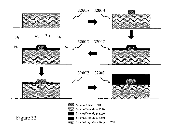
is not
intended to limit the scope, applicability or configuration of the disclosure.
Rather, the
ensuing description of the embodiment(s) will provide those skilled in the art
with an
enabling description for implementing an embodiment or embodiments of the
invention. It
being understood that various changes can be made in the function and
arrangement of
elements without departing from the spirit and scope as set forth in the
appended claims.
Accordingly, an embodiment is an example or implementation of the inventions
and not the
sole implementation. Various appearances of "one embodiment," "an embodiment"
or "some
embodiments" do not necessarily all refer to the same embodiments. Although
various
features of the invention may be described in the context of a single
embodiment, the features
may also be provided separately or in any suitable combination. Conversely,
although the
invention may be described herein in the context of separate embodiments for
clarity, the
invention can also be implemented in a single embodiment or any combination of
embodiments.
100801 Reference in the specification to "one embodiment", "an embodiment",
"some
embodiments" or "other embodiments" means that a particular feature,
structure, or
characteristic described in connection with the embodiments is included in at
least one
embodiment, but not necessarily all embodiments, of the inventions. The
phraseology and
terminology employed herein is not to be construed as limiting but is for
descriptive purpose
only. It is to be understood that where the claims or specification refer to
"a" or "an" element,
such reference is not to be construed as there being only one of that element.
It is to be
understood that where the specification states that a component feature,
structure, or
- 20 -
CA 03119371 2021-05-10
WO 2020/093136
PCT/CA2019/000156
characteristic "may", "might", "can" or "could" be included, that particular
component,
feature, structure, or characteristic is not required to be included.
[00811 Reference to terms such as "left", "right", "top", "bottom", "front"
and "back" are
intended for use in respect to the orientation of the particular feature,
structure, or element
within the figures depicting embodiments of the invention. It would be evident
that such
directional terminology with respect to the actual use of a device has no
specific meaning as
the device can be employed in a multiplicity of orientations by the user or
users.
[0082] Reference to terms "including", "comprising", "consisting" and
grammatical variants
thereof do not preclude the addition of one or more components, features,
steps, integers or
groups thereof and that the terms are not to be construed as specifying
components, features,
steps or integers. Likewise, the phrase "consisting essentially of', and
grammatical variants
thereof, when used herein is not to be construed as excluding additional
components, steps,
features integers or groups thereof but rather that the additional features,
integers, steps,
components or groups thereof do not materially alter the basic and novel
characteristics of the
claimed composition, device or method. If the specification or claims refer to
"an additional"
element, that does not preclude there being more than one of the additional
elements.
100831 Duplex communication over a pair of optical fibers is a common feature
of many
optical communication networks. For example, these may be what are referred to
as "up" /
"down" links between two elements of an optical network, e.g. a remote node
and a central
office, or they may be what are referred to as "east"/ "west" links such as
between nodes on a
ring-based network. Generally, these two optical fibers are routed differently
physically, e.g.
different optical fiber cables, different geographic routes, etc. so that a
fallback fiber, a third
fiber, can provide backup in the event that either of the two fibers fails. Co-
locating the pair
of fibers increases the likelihood that both will fail at the same time and
hence both must be
backed up. Accordingly, different physical routing is common with the third
fiber taking a
different physical path to either of the other pair of optical fibers.
[0084] Referring to Figure 1 there are depicted first to sixth images 100A to
100G
respectively with respect to the implementation of a 2x3 optical switch for
dual fiber optical
link protection using 1x2 switch elements implemented using conventional prior
art IO-
MEMS 1x2 switch elements. Accordingly, first to third images 100A to 100C
depict the
block circuit diagram for the three 2x3 switch configurations in "normal" and
first and second
"fail-over" configurations respectively. Fourth to sixth images 100D to 100F
depict the 2x3
- 21 -
CA 03119371 2021-05-10
WO 2020/093136
PCT/CA2019/000156
optical switch constructed with three 1x2 optical switches 112, 114 and 116.
The
configuration of each of these three 1x2 switches 112, 114 and 116 within the
2x3 optical
switch depicted in the "normal" and first and second "fail-over"
configurations respectively
in first to third switches 110A to 110C respectively in fourth to sixth images
100D to 100F
respectively wherein solid lines represent connections that are "made" or
active and dashed
lines represent connections are "not made" or inactive in each switch
configuration.
[0085] Accordingly, the inventors have established based upon the fact that
there is no need
to ever connect A to D or B to C that it is possible to redesign the switch to
employ a 1x2 and
2x2. Accordingly, referring to Figure 2 there are depicted first to sixth
images 200A to 200F
respectively with respect to the implementation of a 2x3 optical switch for
dual fiber optical
link protection using 1x2 switch elements implemented using conventional prior
art 1 x2 and
2x2 10-MEMS switch elements. Accordingly, first to third images 200A to 200C
depict the
block circuit diagram for the three 2x3 switch configurations such as
discussed supra in
respect of Figure 1. Fourth to sixth images 200D to 200F depict the 2x3
optical switch
constructed with 1x2 optical switch 214 and 2x2 optical switch 212. The
configuration of
these switches within the 2x3 optical switch being depicted by first to third
switches 210A to
210C respectively in fourth to sixth images 200D to 200F respectively wherein
solid lines
represent connections that are "made", or active and dashed lines represent
connections are
"not made" or inactive.
[0086] Now referring to Figure 3 there are depicted first to third image 300A
to 300C
respectively depicting the normal and "fail-over" protection modes for a dual
fiber optical
communications link protected by a third optical fiber, exploiting a pair of
identical 2x3
optical switches on both ends of the optical link comprising first and second
fibers Fiber 1
and Fiber 2 respectively together with the protection "fail-over" optical
fiber, Fiber 3. In first
image 300A the normal operation of the link is depicted showing the first
optical switch in
state 110A and second optical switch in state 120A wherein traffic is carried
from port A to
port A' (or vice-versa) by Fiber 1 and second traffic is carried from port B
to port B' (or vice-
versa) by Fiber 2. First states 110A and 120A are a common switch state for
the pair of 2x3
optical switches. Subsequently, upon traffic upon Fiber 2 being disrupted a
reconfiguration of
the two optical switches re-routes the second traffic on Fiber 2 to Fiber 3.
This is being
depicted in second image 300B wherein the first optical switch is now in state
110B whilst
the second optical switch is in state 120B, these states 110B and 120B being
another common
- 22 -
CA 03119371 2021-05-10
WO 2020/093136
PCT/CA2019/000156
state of the pair of 2x3 optical switches. Accordingly, should traffic be
disrupted on Fiber 2,
then the traffic would be switched onto Fiber 3. Accordingly, on the first
switch the traffic
to/from ports A and B are routed from/to ports C and E respectively whereas on
the second
switch the traffic to/from ports C' and E' are routed from/to ports A' and B'
respectively.
Alternatively, in an alternate fail-over the traffic on Fiber 1 is disrupted
and reconfiguration
of the two optical switches would be configured together to switch the traffic
from Fiber 1
onto Fiber 3.
[0087] This being depicted in third image 300C wherein the first optical
switch is now in
state 110C whilst the second optical switch is in state 120C, these states
110C and 120C
being another common state of the pair of 2x3 optical switches. Accordingly,
with traffic
disrupted on Fiber 1 the traffic is routed to Fiber 3 which is implemented on
the first switch
such that the traffic to/from ports A and B are routed from/to ports E and D
respectively
whereas on the second switch the traffic to/from ports E' and D' are routed
from/to ports A'
and B' respectively. These configurations being listed in Tables 1 to 3
respectively below.
Left Switch Right Switch
Input Port Connected To Output Port Connected To
A C A' C'
B' D'
Table 1: Normal Mode
Left Switch Right Switch
Input Port Connected To Output Port Connected To
A C A' C'
B' E'
Table 2: Protection for Fiber 2 Failure
Left Switch Right Switch
Input Port Connected To Output Port Connected To
A E A' E'
B' D'
Table 3: Protection for Fiber 1 Failure
[0088] Referring back to Figure 2 and the 2x2 optical switch 212 within fourth
to sixth
images 200D to 200F respectively for the "normal" operating mode and the two
"fail-over
- 23 -
CA 03119371 2021-05-10
WO 2020/093136
PCT/CA2019/000156
conditions" then it is evident that whilst it is configured in both of, what
are commonly
referred to as, the "bar state" and "cross state" configurations but that
there is no requirement
for both "cross" paths to be employed in any configuration. Accordingly, the
inventors have
established that a IO-MEMS based design where the first IO-MEMS is used only
as a 1x2
switch element and the second 10-MEMS 212 is only used for the functionality
of "simple"
crossbar switch element rather than a full 2x2 doesn't need can be implemented
with a
second IO-MEMS 212 in the form of a crossbar rather a 2x2. Accordingly,
referring to Figure
4 there is depicted according to an embodiment of the invention an
implementation of a 2x3
optical switch for dual fiber optical link protection implemented using an IO-
MEMS based
"horseshoe" configuration optical switch according to an embodiment of the
invention. The
inventors referring to the IO-MEMS design as "horseshoe" as each optical path
within the
IO-MEMS elements loops back, as does a horseshoe, wherein the horseshow can
either
implement 1x2 or crossbar functionality.
10089] Accordingly, Figure 4 depicts the internal implementation of a 2x3
optical switch
"horseshoe" IO-MEMS (2x3 HS-1O-MEMS) circuit 400 for dual fiber optical link
protection
via a third optical fiber, wherein the 2x3 optical switch circuit 400 is
composed of two IO-
MEMS elements, a first IO-MEMS element 420A providing the 1x2 switch
functionality,
equivalent to 1x2 switch 214 in fourth to sixth images 200D to 200F
respectively in Figure 2,
and a second IO-MEMS element 430B providing the required functionality of the
crossbar
switch, thus allowing the circuit 400 to replace the 2x2 switch 212 in fourth
to sixth images
200D to 200F respectively in Figure 2. Accordingly, these are depicted in
first to third images
400A to 400C in Figure 4 for the "normal" state 110A and the two protected
states 110B and
110C respectively. In first image 400A the first and second 10-MEMS elements
are depicted
as first IO-MEMS 420A and second IO-MEMS 430A which represent the first and
second
IO-MEMS elements in non-actuated state. In second image 400B the first IO-MEMS
element
is still in its non-actuated state, depicted as first 10-MEMS 420A, whilst the
second 10-
MEMS element is in an actuated state, depicted as third 10-MEMS 430B. In third
image
400C the first IO-MEMS element is now in its actuated state, depicted as
fourth IO-MEMS
420B whilst second 10-MEMS element is in its non-actuated state 430A.
Accordingly, as
evident in first to third images 400A to 400C respectively there are no
waveguide crossings
within the 2x3 switch optical switch circuit 400 which arises from the limited
active optical
path configurations of the crossbar optical switches 430A and 420B.
- 24 -
CA 03119371 2021-05-10
WO 2020/093136
PCT/CA2019/000156
[0090] Accordingly, within first to third images 400A to 400C of the 2x3 HS-10-
MEMS in
the three switch configurations. First image 400A depicts the 2x3 HS-IO-MEMS
in the
normal configuration with ports A and B coupled to ports C and D respectively
and Fiber 1 /
Fiber 2 active. Accordingly, the 2x3 HS-IO-MEMS comprises a substrate with a
plurality of
three-dimensional (3D) optical waveguides from ports denoted A, B, C, D, and E
which are
coupled to the first and second IO-MEMS elements which are themselves
interconnected via
appropriate waveguide routing while exploiting 3D optical waveguides. Within
this
embodiment the waveguides exploit 90 degree turning mirrors rather than
waveguide bends,
but such 3D waveguides could exploit waveguide bends. Further, such waveguides
could be
routed and/or implemented at any arbitrary angle at the interface between the
fixed and
suspended portions of the IO-MEMS as will be further explained later in Figure
7. In second
image 400B the first IO-MEMS element is maintained in the same configuration,
but the
second 10-MEMS element has been moved right one "stop" such that the second IO-
MEMS
element is coupled to a different subset of the plurality of 3D optical
waveguides on the
substrate such that the 2x3 HS-IO-MEMS provides the appropriate routing of
port A to port
C and port B to port E.
[0091] In third image 400C the first IO-MEMS element has now been moved left
one "stop"
but second LO-MEMS element 420A is in its original configuration as in first
image 400A.
Accordingly, the first IO-MEMS element is coupled to a different subset of the
plurality of
3D optical waveguides on the substrate such that the 2x3 HS-IO-MEMS provides
the
appropriate routing of port A to port E and port B to port D. Accordingly, the
2x3 HS-10-
MEMS is configured solely based upon lateral motion of the first and second IO-
MEMS
elements.
[0092] Now referring to Figures 5A to 5C respectively there are depicted the
normal mode
and the two "fail-over" protection modes for a dual fiber optical
communications link
protected by a third optical fiber, exploiting identical 2x3 HS-IO-MEMS 400 on
both ends of
the link sharing a common state in each mode of operation. Considering Figure
5A for the
normal operation of the link (state 410A for the left switch and state 510A
for the right
switch) each 2x3 HS-IO-MEMS is configured as depicted in first image 400A of
Figure 4,
i.e. each IO-MEMS element is non-actuated. Accordingly, the optical signals
from Ports 1
and 2 are routed to/from Ports 3 and 4 via Fiber 1 and Fiber 2.
- 25 -
CA 03119371 2021-05-10
WO 2020/093136
PCT/CA2019/000156
[0093] In Figure 5B a first fail-over mode is depicted wherein each 2x3 HS-IO-
MEMS is
configured as depicted in second image 400B of Figure 4, i.e. the first 10-
MEMS element has
been actuated whilst the second JO-MEMS element is non-actuated. Accordingly,
the optical
signals from Ports 1 and 2 are routed to/from Ports 3 and 4 via Fiber 1 and
Fiber 3
respectively. In Figure 5C a second fail-over mode is depicted wherein each
2x3 HS-10-
MEMS is configured as depicted in second image 400C of Figure 4, i.e. the
first IO-MEMS
element is non-actuated whilst the second IO-MEMS element is actuated.
Accordingly, the
optical signals from Ports 1 and 2 are routed to/from Ports 3 and 4 via Fiber
2 and Fiber 3
respectively.
[0094] Referring to Figures 6A and 6B there are depicted first and second
alternate
configurations 600 and 650 for a 2x3 HS-IO-MEMS optical switch according to an
embodiment of the invention exploiting waveguide bends rather than turning
mirrors. The
exact design of the waveguide bends may vary in dependence upon factors such
as
geometrical constraints and waveguide index contrast. Waveguide index contrast
of the 3D
optical waveguides can vary from low contrast (low confinement), such as Si02-
S13N4-
Si02, to higher contrast (higher confinement) stemming from use of a
rectangular waveguide
core or further through high index contrast materials selection such Si core
with SiO2
cladding (typical of conventional silicon photonics platforms). As index
contrast and
confinement increased tighter lower radius bends can be employed within the 3D
optical
waveguides. Within first image 600 the TO-MEMS elements are configured in
common with
those depicted in Figures 4 and 5. However, in second image 650 the first and
second IO-
MEMS elements 610 and 620 are orientated vertically in the same orientation
upon a
substrate 610 and similarly exploit waveguide bends rather than turning
mirrors such as
depicted in Figure 4. Finally, such waveguides could be routed implemented at
any arbitrary
angle at the interface between the fixed and suspended portions of the 10-MEMS
as will be
further explained later in Figure 7.
[0095] Referring to Figure 6B, there is depicted a waveguide routing
arrangement between
two instances of the 1IS-IO-MEMS enabling the routing of the optical switch in
a manner
which allows the duplication of this arrangement in a large M x N array
enabling the use of
the HS-10-MEMS in a larger scale matrix optical switch may further conform to
a path
independent loss topology by placing waveguide crossings between HS-I0-MEMS
instances.
- 26 -
CA 03119371 2021-05-10
WO 2020/093136
PCT/CA2019/000156
[0096] Now referring to Figure 7 there is depicted an exemplary die layout for
a lx4 optical
switch exploiting a HS-!O-MEMS optical switch according to an embodiment of
the
invention. Accordingly, as the HS-IO-MEMS comprises:
= Substrate 710;
= Input waveguide 720;
= Output waveguides 730;
= Shuttle 740, upon which the waveguide layout to connect the input
waveguide to each output of the output waveguides 740 when it moves
laterally and/or vertically, wherein the waveguides on the Shuttle 740 have
been omitted for clarity and can be routed and/or implemented at any
arbitrary angle to match the angles of the Input waveguides 720 and Output
waveguides 730, enabling for instance the reduction of the waveguide bend
on the shuttle 740;
= Gap closer MEMS spring 750 to move the shuttle 740 away from the
waveguides
during reconfiguration and towards the waveguides after reconfiguration is
complete, this being under electrostatic action from gap closer 780;
= First and second lateral MEMS actuators 760A and 760B to move the shuttle
laterally under electrostatic action; and
= First and second stop actuators 770A and 770B which define the limit of
lateral
motion for the different configurations, under electrostatic action
[0097] As depicted the I x4 HS-10-MEMS has a series of pads for application of
the
appropriate electrical voltages to provide the target electrostatic action,
these being, in
addition to ground (GND):
= VDD directional displacement voltage;
= GC gap closer voltage;
= STO3 31.1m stopper actuation; and
= STO6 6nm stopper actuation.
100981 Accordingly, if STO3 is applied the first and second stop actuators
770A and 770B
allow a lateral motion of 311m from the initial displacement position of the
shuttle 740 when
VDD=OV. If 5T06 is applied the first and second stop actuators 770A and 770B
allow a
lateral motion of 6nm from the initial displacement position of the shuttle
740 when
VDD=OV. If neither STO3 or STO6 are applied the first and second stop
actuators 770A and
- 27 -
CA 03119371 2021-05-10
WO 2020/093136
PCT/CA2019/000156
770B allow a lateral motion of 9Am from the initial displacement position of
the shuttle 740
when VDD=OV. The shuttle 740 motion being unidirectional to the left from its
initial
position.
[0099] However, in Figure 7B a variant 1x4 {S-IO-MEMS is depicted wherein
bidirectional
motion of the shuttle 740 is provided as the second lateral MEMS actuator 760B
is
"reversed" relative to the first lateral MEMS actuator 760A such that
application of a VDD
signal to the associated with second lateral MEMS actuator 760B rather than
those associated
with first lateral MEMS actuator 760A results in motion in the other
direction. Also
associated with the reversal of the second MEMS actuator 760B are third and
fourth stop
actuators 770C and 770D respectively which provide stops for motion of the
shuttle in the
other direction at the same motion limits (although different motion limits
may be established
for left and right motion if appropriate.
1001001 Referring to Figure 8 there is depicted an exemplary design for
a
programmable switch state stopper for a MEMS based device such as first and
second stop
actuators 770 and 770B respectively in Figure 7A and first to fourth stop
actuators 770A to
770D respectively in Figure 7B. First image 800A depicts the stop actuator
with its tip 850
and beam 830. Second to fourth images 800B to 800D respectively depict the
stop actuator
when actuated for 311m and 611m motion and unactuated for 9Am using the
configuration
described and depicted within Figures 7A and 7B respectively. In each there
are depicted first
and second side electrodes 810 and 820 which are depicted in first image 800A
running along
the length of the beam 830, beam 830 with shaped tip, and stop contact 840
which as
depicted in Figures 7A and 7B is connected to ground. First side electrode 810
being coupled
to STO3 such that when the actuation voltage is applied to the STO3 pad the
beam 830 is
attracted electrostatically to the first side electrode 810. Second side
electrode 820 being
coupled to STO6 such that when the actuation voltage is applied to the STO6
pad the beam
830 is attracted electrostatically to the second side electrode 820. When no
voltage is applied
to either first side electrode 810 and second side electrode 820 then the beam
is in the middle
not attracted to either.
[00101] Accordingly, depending upon whether the beam is in the middle
or attracted
up / down then a different portion of the beam 830 at its tip will contact the
stop contact 840
as the shuttle 740 is moved laterally. Whilst discrete electrostatic actuation
with two
electrodes is depicted in Figures 7A to 8 respectively it would be evident
that within other
- 28 -
CA 03119371 2021-05-10
WO 2020/093136
PCT/CA2019/000156
embodiments of the invention that the number of stops may be increased by
increasing the
number of steps in the stop actuator tip and/or stop contact in conjunction
with multiple
actuator voltages or that multiple actuators may be employed each offering,
for example a
first stop with actuation of the upper electrode, a second stop with actuation
of the lower
electrode and unrestricted motion with neither actuated. Alternatively,
multiple stop actuator
along a single common beam mean be employed which are individually actuated.
Optionally,
rather than discrete "on/off' actuators such as those depicted in Figures 7A
to 8 a tunable
actuator, e.g. an electrostatic linear comb drive for example, may be employed
wherein
tolerance on the voltage to the comb drive for each stop is provided through
the overlap
between the actuator elements. For example, considering second image 800B in
Figure 8 then
once a predetermined voltage is exceeded the beam 830 engages the stop contact
840 and
increasing the voltage whilst further pulling the beam 830 does not adjust the
action of the
stop actuator.
1001021 Within the embodiments of the invention described and depicted
in respect of
Figures 4 to 8 the optical waveguides are non-overlapping and each couple a
first port of a
plurality of ports on one side of the shuttle to a second port of the
plurality of ports on the
same side of the shuttle. However, within other embodiments of the invention
the optical
waveguides in order to provide the required optical functionality may overlap
(i.e. cross one
another) or they may route to the other side of the shuttle distal to the side
they originate on
(or vice-versa terminate on). Accordingly, different programmable optical
interconnects may
be implemented. It would be further evident that whilst the embodiments of the
invention
described and depicted in respect of Figures 4 to 8 exploit a pair of shuttles
that other designs,
such as a simple optical lxN switch may exploit a single shuttle whilst others
may exploit 3,
4, or more with different interconnections (mappings) between the multiple
shuttles.
1001031 Figures 7A to 8 describe and depict stops for lateral motion of the
shuttle 740
during its movement. Now referring to Figures 9A to 9C there are depicted
exemplary
designs for stoppers for defining the gap under closure of the gap closers
within MEMS
based optical switches according to an embodiment of the invention. Figure 9A
depicts the
configuration shown in Figures 7A and 7B wherein the shuttle under action of
the gap closer
780 moves either towards the gap closer 780 when electrostatic attraction
exists or is pulled
back under action of the gap closer MEMS spring 750. Accordingly, the
waveguides are
formed onto the stoppers at either side, Stopper 1 910 and Stopper 2 920
whilst the Shuttle
- 29 -
CA 03119371 2021-05-10
WO 2020/093136
PCT/CA2019/000156
940A is moved towards these under electrostatic attraction arising from the
Gap Closer 930A.
In order that the Stopper 1 910 and Stopper 2 920 define the limit of the
Shuttle 940A under
action of the Gap Closer 930A the Gap Closer 930A is "recessed" away such that
it cannot
contact the Shuttle 940A.
[00104] Alternatively, in Figure 9B an alternate design is employed wherein
first and
second pairs of stoppers 910A/9 10B and 920A/920B are depicted and engage
against stops
950 upon the shuttle 940B with the Gap Closer 930B recessed again. Whilst the
first and
second pairs of stoppers 910A/910B and 920A/920B and stops 950 are depicted as
square in
Figure 9B it would be evident that within other embodiments of the invention
the designs for
these may vary to include other geometries. Optionally, within another
embodiment of the
invention the stops and stoppers may be tapered such that the shuttle 940B is
aligned to the
stops in a form of "self-aligning" so that as the gap closer closes the gap
the shuttle 940B
engages the stoppers and "aligns" via the stops 950. Optionally, within other
embodiments of
the invention the stoppers may be movable rather than fixed using actuators
such as, for
example, parallel plate actuators, comb drive actuators etc. Optionally,
multiple stoppers may
be moved together or independently from one another. As the stoppers will,
typically, have
the optical waveguides upon them to butt couple to optical waveguides upon the
shuttle 940B
then within other embodiments of the invention the stoppers may be movable,
and the shuttle
fixed, or both the stoppers and the shuttle may be movable.
[00105] Within Figure 9C an alternate design is depicted wherein first and
second pairs of
stoppers 910C/910D and 920C/920D are depicted together with first and second
stops 970
and 980 which now are at varying offsets from the gap closer 930C.
Accordingly, the stops
define different stop positions for the shuttle 940C when it moves laterally
with respect to the
stops. Whilst the stops are depicted parallel to the stoppers in Figure 9C
within other
embodiments of the invention one or more of the stoppers may be orientated at
an angle
relative to the motion of the shuttle 940C with laterally under action of the
first and second
lateral MEMS actuators 760A and 760B respectively or relative to the motion of
the shuttle
940C under the action of the gap closer 930B. Optionally, within another
embodiment of the
invention the stops and stoppers may be tapered such that the shuttle 940C is
aligned to the
stops in a form of "self-aligning" so that as the gap closer closes the gap
the shuttle 940C
engages the stoppers and "aligns" via the stops 970. Optionally, within other
embodiments of
the invention the stoppers may be movable rather than fixed using actuators
such as, for
- 30 -
CA 03119371 2021-05-10
WO 2020/093136
PCT/CA2019/000156
example, parallel plate actuators, comb drive actuators etc. Optionally,
multiple stoppers may
be moved together or independently from one another. As the stoppers will,
typically, have
the optical waveguides upon them to butt couple to optical waveguides upon the
shuttle 940B
then within other embodiments of the invention the stoppers may be movable,
and the shuttle
fixed, or both the stoppers and the shuttle may be movable.
[00106] Within the embodiments of the invention described and depicted with
respect to
Figures 4A to 9C the 3D optical waveguides on the fixed portion of the IO-MEMS
"butt-
couple" to the 3D optical waveguides on the moving portion of the 10-MEMS.
Butt-coupling
being where the two optical waveguides "butt" against each other although the
term is also
used to refer to optical coupling between two optical waveguides with a small
gap between
them. Within embodiments of the invention the stoppers may define a
predetermined gap or
no gap to be between the 3D optical waveguides when the gap closer brings the
moving
portion of the 10-MEMS to the fixed portion of the IO-MEMS. Optionally, the 3D
optical
waveguides may exploit optical tapers or multi-mode interferometers (MMIs) to
expand the
optical mode size at the interfaces thereby improving coupling tolerances
and/or reducing
coupling losses. Optionally, the waveguides may exploit micro-lenses fused
onto or formed
from the end faces of the 3D optical waveguides through a process such as a
laser-based
process, for example.
[00107] Referring to Figure 10 there are depicted exemplary optical interfaces
between a
static portion of an IO-MEMS circuit and the moveable MEMS element forming
part of the
IO-MEMS circuit. As depicted a movable MEMS element 1040 has a 3D optical
waveguide
1070 disposed upon it which is coupled to first and second optical waveguides
1060A and
1060B respectively upon first and second static elements 1010 and 1020 of the
10-MEMS
circuit. First optical interface 1000A couples the first optical waveguide
1060A upon first
static element 1010 to the 3D optical waveguide 1070 via an MMI coupler
comprising first
and second portions 1050A and 1050B wherein when these abut each other under
action of
the MEMS actuator closing the gap between the first and second static elements
1010 and
1020 with movable MEMS element 1040 they form the MMI such that optical
signals are
coupled to/from the 3D optical waveguide 1070 from/to the optical waveguide
1060A. In
contrast in second optical interface 1000B the second optical waveguide 1060B
is coupled to
the 3D optical waveguide 1070 via first and second optical waveguide tapers
1050C and
1050D respectively.
- 31 -
CA 03119371 2021-05-10
WO 2020/093136
PCT/CA2019/000156
[00108] Within the embodiments of the invention described and depicted in
respect of
Figures 4A to 10 10-MEMS devices supporting reconfiguration of the optical
connectivity
have been described exploiting fixed portions and a movable portion wherein
the movable
portion has 3D optical waveguides upon it such that the motion of the movable
portion
relative to the fixed positions results in the connectivity changes. However,
within other
embodiments of the invention the moving portion of the 10-MEMS is a flexible
waveguide
which moves from a first position to a second position such that it couples to
different 3D
optical waveguides upon another fixed portion of the 10-MEMS. An exemplary
embodiment
of the invention is described and depicted in Figures 11A and 11B with respect
to a 2x2 TO-
MEMS switch.
[00109] Accordingly, referring to Figure 11A there is depicted a 2x2 IO-MEMS
switch
according to an embodiment of the invention in a bar state exploiting what the
inventors refer
to as Thin Beam Unsupported Waveguide (THAW) 10-MEMS actuators. Accordingly,
are
depicted four anchors, IN1 1105A, OUT1 1105B, IN2 1105C, and OUT2 1105D. Each
of
these extends with a MEMS beam 1115 which is coupled to a MEMS actuator 1110
and
supports a 3D optical waveguide 1190. Disposed centrally to the four anchors
is a fixed
portion 1140 of the IO-MEMS comprising a pair of bar waveguides 1170 and a
pair of cross
waveguides 1180. At each corner of the fixed portion 1140 of the IO-MEMS are
first and
second stops 1120 and 1130 together with bar electrode 1155 and cross
electrode 1165. The
bar electrodes 1155 are connected to the electrode pads VDD Bar 1150 and the
cross
electrodes 1165 are connected to the electrode pads VDD Cross 1160. As
depicted in Figure
11A drive voltages are applied to electrode pads VDD Bar 1150 such that the
MEMS beams
1115 are electrostatically attracted to the bar electrodes 1155 and against
first stops 1120 such
that the 3D optical waveguides 1190 are coupled to the bar waveguides 1170. In
Figure 11B
the drive voltages are applied to the electrode pads VDD Cross 1160 such that
the MEMS
beams 1115 are electrostatically attracted to the cross electrodes 1165 and
against second
stops 1130 such that the 3D optical waveguides 1190 are coupled to the cross
waveguides
1180.
[00110] Alternatively, Figure 11C depicts actuator configurations for a 2x2 10-
MEMS
optical switch according to an embodiment of the invention with "blocked"
power fail state
(or default MEMS state) and driven "cross" and "bar" states. In this
configuration the initial
or non-actuated position for the THAW 10-MEMS actuators with a 3D optical
waveguide.
- 32 -
CA 03119371 2021-05-10
WO 2020/093136
PCT/CA2019/000156
Accordingly, first to third images 1100C to 1100E depict a MEMS beam 11100
with optical
waveguide, first electrode 11200 and second electrode 11300. In first image
1100C no
voltage is applied to either the first electrode 11200 or the second electrode
11200 such that
the MEMS beam 11100 is not deformed. In second image 1100D the drive voltage
is applied
to the second electrode 11300 such that the MEMS beam 11100 is deformed by
electrostatic
attraction to the second electrode 11300. In third image 1100E the drive
voltage is applied to
the first electrode 11200 such that the MEMS beam 11100 is deformed by
electrostatic
attraction to the first electrode 11200. Accordingly, where this actuation
scheme is employed
with a 2x2 IO-MEMS the first image 1100C represents no optical coupling
between the
optical waveguide on the MEMS beam 11100 to any waveguides of the 10-MEMS. In
contrast in second and third images 1100D and 1100E the optical waveguide on
the MEMS
beam 11100 to waveguides of the IO-MEMS, such as bar waveguides 1170 and cross
waveguides 1180 as depicted in Figures 11A and 11B respectively.
1001111 It would be evident that within other embodiments of the invention
that the initial
THAW 10-MEMS actuator position and hence that also the power fail state may be
in a
defined switch state or coupling condition for the THAW IO-MEMS actuator.
Considering
Figures 11A and 11B then the cross state condition of the switch may be
established if the
THAW IO-MEMS actuator is aligned to the cross waveguide 1180 without any
applied
voltage, e.g. VDD Cross = OV. Accordingly, the switch only requires activation
for
implementing the bar state. Alternatively, the THAW IO-MEMS actuator may be
initially
fabricated to align with the bar waveguide 1170 such that activation is only
required for the
cross state. It would be evident that in other embodiments of the invention
different
configurations of THAW IO-MEMS actuator may be employed such that, for
example, the
THAW IO-MEMS actuators associated with 1N1 1105A and IN2 1105C are aligned in
one
position with respect to bar and cross waveguides 1170 and 1180 respectively
whilst the
OUT1 1105B and OUT2 1105D THAW 10-MEMS actuators are aligned to a different
position.
[00112] It would be evident that different optical devices may be implemented
using the
THAW IO-MEMS actuators in conjunction with or without mechanical stops.
Optical
devices may also exploit different numbers and combinations of THAW 10-MEMS
actuators.
Further THAW 10-MEMS actuators within the same optical device may provide
different
"functions" in combination with the optical waveguides to which they couple
such as
- 33 -
CA 03119371 2021-05-10
WO 2020/093136
PCT/CA2019/000156
attenuator, on-off switch, and route selector with 2, 3, 4 or more routes for
example. Whilst
electrostatic actuation for low complexity THAW 10-MEMS actuators has been
described
and depicted it would be evident that other actuation means may be employed
for the THAW
10-MEMS actuators such as thermal actuation, rotational electrostatic comb
drive and
rotational electrostatic comb drive, and circular electrostatic comb drive for
example.
[00113] Now referring to Figures 12A there is depict an unpowered, non-
deformed,
configuration for a 2x2 MEMS optical switch exploiting THAW IO-MEMS actuators
with
direct deformable arm positioning according to an embodiment of the invention
without
intermediate 3D optical waveguides that are fixed. Accordingly, are depicted
four anchors,
IN! 1205A, OUT! 1205B, IN2 1205C, and OUT2 1205D. Each of these extends with a
MEMS beam 1230 which is coupled to a MEMS actuator 1220 and supports a 3D
optical
waveguide 1210. At the ends of each beam 1230 coupled to the IN1 1205A and IN2
1205C
anchors there is a first stop 1260 disposed whilst at the ends of each beam
1230 coupled to
the OUT1 1205B and OUT2 1205D anchors there is disposed a second stop 1270.
Disposed
to either side of each MEMS beam 1230 are bar electrode 1220A and cross
electrode 1220B
which are coupled to bar electrode pads 1240 and cross electrode pads 1250
respectively.
Accordingly, as depicted in Figure 12B the appropriate drive voltage, VDD Bar,
is applied to
the bar electrode pads 1240 wherein the MEMS beam 1230 is electrostatically
attracted to the
bar electrode 1220A in each instance. As the MEMS beams 1230 flex then the
tips orientate
with respect to each other through the first stop 1260 and second stop 1270.
Similarly, in
Figure 12C the appropriate drive voltage, VDD Cross, is applied to the bar
electrode pads
1250 wherein the MEMS beam 1230 is electrostatically attracted to the cross
electrode
1220B in each instance. As the MEMS beams 1230 flex then the tips orientate
with respect to
each other through the first stop 1260 and second stop 1270.
[00114] Optionally, within other embodiments of the invention the MEMS beams
1230 may
be electrostatically charged rather than the bar electrodes 1220A or cross
electrodes 1220B.
Alternatively, the bar electrodes 1220A and cross electrodes 1220B may be
oppositely
charged relative to the MEMS beam 1230 to attract or similarly charged to
repulse.
Optionally, within other embodiments of the invention the MEMS arms 1230 may
be
directly, i.e. physically, moved through an actuator directly rather than
indirectly moved via
an attraction / repulsion mechanism. Such direct actuation may, for example,
exploit one or
- 34 -
CA 03119371 2021-05-10
WO 2020/093136
PCT/CA2019/000156
more parallel plate MEMS actuators, one or more MEMS comb drive actuators, one
or more
MEMS circular comb drive actuators, etc.
[00115] Amongst the challenges of packaging optoelectronic circuits, photonic
circuits,
integrated optical circuits, JO-MEMS, etc., referred to generally as photonic
integrated
circuits (PICs), is the positioning of the optical fiber(s) being coupled to
the PLC. This is
problematic even with a single optical fiber (fiber) but even more complex
where multiple
optical fibers (fibers) are to be connected to the PIC, especially on the same
side of the PIC
die as generally optical fibers require a pitch (spacing) at the die edge that
is larger than the
pitch of the 3D optical waveguides on the PIC die. Within the prior art to
remove handling
issues of multiple fibers ribbon optical fibers were developed to provide, for
example, 4, 6, 8,
or 12 fibers within a single ribbon. Whilst this improves handling of multiple
fibers the
preparation of the fibers for optical coupling to the PIC raises an additional
issue in that in
order to provide the multiple fibers with a common end plane for mating to the
PIC the
ribbon is typically assembled into another assembly and the end polished, such
as employed
in ribbon fiber connectors. However, amongst the techniques for aligning
optical fibers to a
PLC is the use of U-shaped grooves (U-grooves) or V-shaped grooves (V-groove)
formed into
a substrate, this substrate may be the PLC substrate itself within or upon
which the PLC is
formed upon or it may be another substrate to which substrate the PLC is
formed upon is
attached to. However, these preclude the use of polished fiber assemblies
unless the fibers
can be polished and project beyond the end of the assembly they are assembled
within.
However, cleaving (providing a high-quality end face through inducing a crack
in the optical
fiber which is then propagated through the fiber) a ribbon fiber results in a
variation in the
end positions of each fiber within the ribbon.
[00116] Accordingly, the inventors have established a PLC design approach that
allows the
PIC to accommodate the length variation within the cleaved fiber ribbon.
Accordingly, as
depicted in Figure 13A in first image 1300A the concept, referred to as
flexible edge connect
(FLEC) by the inventors, comprises a suspended platform 1370 which abuts the
end face of
the optical fiber 1310 when the fiber is inserted into a U-groove or V-groove
which is
depicted simply by edge features 1320 (these being patterned portions of the
PIC layer stack
deposited onto the substrate within which the U-groove or V-groove is formed.
In Figure 13A
the fiber end face is depicted at a separation d1 from the end of the
suspended platform 1370.
Disposed either side of the suspended platform 1370 are ratchet structures
1350 which are
- 35 -
CA 03119371 2021-05-10
WO 2020/093136
PCT/CA2019/000156
coupled to mounts 1330 via hinges 1380. The suspended platform 1370 is
attached to anchor
portions 1340 via flexible anchors 1360. Accordingly, an optical waveguide
(not depicted for
clarity) can be formed upon the suspended platform 1370 and routed via one of
the flexible
anchors 1360 to the PIC.
[001171 In second image 1300B the ratchet 1350 structure is depicted in detail
comprising
first section 1350A attached to the hinge 1380 and second section 1350B
forming part of the
suspended platform 1370. Depicted are a series of teeth 1350C such that as the
second section
1350B is moved right relative to the first section 1350A the hinge allows the
second section
1350B to move relative to the first section 1350A but cannot reverse
direction.
1001181 Referring to Figure 13B the optical fiber 1310 is inserted into the U-
groove or V-
groove and abuts the suspended platform 1370 wherein it may be "pushed" such
that the
suspended platform 1370 moves, the ratchet structures 1350 allowing motion of
the
suspended platform forward wherein the teeth engage to restrict motion of the
suspended
platform 1370 backwards beyond the last tooth engaged.
[001191 This is depicted in the instance of a pair of fibers 1310A and 1310B
in Figure 14A
which are inserted into grooves, not depicted for clarity but indicated by
first to third
patterned regions 1430 to 1450 respectively. Also depicted are first and
second FLEC
structures 1410B and 1420B respectively. The pair of fibers 1310A and 1310B
being within a
ribbon and having an offset, doFFsEr, between their end faces. Next, in Figure
I4B the pair of
fibers 1310A and 1310B have been inserted and pushed forward so that they
engage the first
and second FLEC structures 1410B and 1420B respectively. Accordingly, the
offset between
the pair of fibers 1310A and 1310B, doFFsET, is reflected in the same offset
in the suspended
platforms 1370 within each of the first and second FLEC structures 1410B and
1420B
respectively. Accordingly, the first flexible anchor 1430 in first FLEC
structure 1410A is
deformed by a first amount and the second flexible anchor 1440 in second FLEC
structure
1410B is deformed further by a second amount as it accommodates the offset,
domEr=
[001201 Optionally, array of grooves (V-grooves or U-grooves) may be defined
such that the
end of the most prominent fiber within the ribbon fiber array, of which first
and second fibers
1310A and 13108 form part, "hits" the end of the groove it is in and pushes
the suspended
platform 1370 the furthest from its initial position. Accordingly, the other
optical fibers do
not push their respective suspended platforms as far forward as the most
prominent optical
fiber. This structure is depicted in Figure 14C wherein the suspended platform
14140 is
- 36 -
CA 03119371 2021-05-10
WO 2020/093136
PCT/CA2019/000156
depicted together with a single flexible structure 14160 with optical
waveguide 14150. Also
evident are the pair of ratchet structures 14110 that allow the suspended
platform to move to
the right but not backwards to the left. Also depicted is hinge 14120 attached
to one of the
ratchet structures 14110. Accordingly, the number of teeth on each ratchet
structure may be
defined according to the desired tolerance of locking the ratchet once moved
forward by the
optical fiber.
[00121] Within embodiments of the invention described and depicted in respect
of Figures
7A to 14 above and Figures 16 to 21 below, devices exploiting IO-MEMS
structures have
been described and depicted wherein an optical waveguide is formed atop a MEMS
structure
in order to support dynamic positioning of the optical waveguide on the
suspended portion of
the IO-MEMS relative to a plurality of fixed optical waveguides and/or other
structures. As
noted in respect of photonic integrated circuits (PICs), the management of
stress is important
as vertical deformation of the 10-MEMS beam(s) relative to the fixed waveguide
portions
results in increased insertion loss of the PIC. Accordingly, residual stress
within the MEMS
beam and/or other structures when released from the substrate will result in
deformation of
the MEMS beam and/or other structures. The sensitivity of the optical
waveguide alignment
within an 10-MEMS is such that at residual stress levels far below those
necessary to impact
operation of the MEMS the deformation in the MEMS beam and/or other structures
will
result in increased insertion loss and potentially complete misalignment. As
will become
evident in subsequent descriptions in respect of Figures 16 to 22 below
residual stress also
impacts suspended MEMS / IO-MEMS structures such as the beams within 10-MEMS
described and depicted within Figures 7A to 14C above.
[00122] Accordingly, the inventors have established different manufacturing
methodologies
to address the issue. These being depicted in Figures 16 to 22 respectively
whilst Figure 15
depicts a prior art uncompensated waveguide design such as described and
depicted within
previous patent applications by the inventors including, but not limited to,
PCT/CA2015/000135 entitled " and PCT/CA2015/000136 entitled "." Accordingly,
Figure
15 depicts a cross-section of a fabricated 10-MEMS as described and depicted
within
PCT/CA2015/000135 and PCT/CA2015/000136 comprising:
= Substrate 1500 formed from silicon 1520;
= MEMS 1500A comprising first and second sections 1550A and 1550B;
= Passive waveguide 1500B; and
- 37 -
CA 03119371 2021-05-10
WO 2020/093136
PCT/CA2019/000156
= Bragg waveguide 1500C.
[001231 The first section 1550A of the MEMS 1500A being formed solely from
silicon
1520. Second section 1550B of the MEMS 1500A comprises an optical waveguide
stack atop
the silicon 1520. The optical waveguide stack comprising a lower cladding
(silicon dioxide
1530), core (silicon nitride 1540), and upper cladding (silicon dioxide 1530).
Within the
passive waveguide 1500B and Bragg waveguide 1500C then optical waveguide stack
is atop
the silicon 1520 upper layer and substrate and the intervening buried oxide
(BOX) layer of
silicon dioxide 1530. The depicted design cross-section being of a rotary MEMS
with planar
waveguide coupling optical signals to one or more waveguides with a Bragg
grating. Within
exemplary implementations the thickness, tsi, of the silicon atop the BOX is
25 m.
[001241 Referring to Figure 16 there are depicted exemplary first cross-
section 1600A of
initial starting wafer and second cross-section 1600B of a processed
integrated optics
microelectromechanical system (IO-MEMS) device according to an embodiment of
the
invention for uncompensated mirrorless designs. The inventors refer to this
design concept as
"Small Waveguide on Big" 10-MEMS (SWB-10-MEMS) as a result of two mutually
beneficial factors. Firstly, the removal of the optical stack where there is
no need for
waveguides on the suspended IO-MEMS platform 1660 formed out of the 1610
(silicon
1601) atop the BOX 1620 (SiO2 1602) and secondly the relative thickness of the
device layer
of the 10-MEMS substrate 1630 (silicon 1601). This device layer has a
thickness established
in dependence upon the Optical Fiber 1690 outside diameter thereby enabling
the creation of
a relatively thick suspended mechanical layer for the optical waveguides 1680
and preventing
the waveguides on the suspended portion of the 10-MEMS from vertically
deflecting out of
alignment with the output waveguides on the fixed portion of the TO-MEMS.
Furthermore,
the SWB-IO-MEMS provides for optical fiber 1690 alignment to waveguides 1680
unlike the
prior art geometry depicted in Figure 15. The back of the wafer having an
optional thermally
grown or deposited silicon dioxide 1640 layer (SiO2 1602) for minimizing wafer
bow.
1001251 In second image 1600B the processed device cross-section is depicted
with MEMS
region 1660 with: i) opening 1670 beneath and waveguide geometry 1650
comprising the
fixed 3D optical waveguides atop the substrate 1630, ii) the waveguides atop
the IO-MEMS
1660 comprising, and iii) the movable 3D optical waveguides 1680 on the
suspended portion
of the IO-MEMS. The waveguide geometry 1650 comprising a lower cladding (SiO2
1602),
core (core 1603 such as silicon nitride), and upper cladding (SiO2 1602).
Alternatively, the
- 38 -
CA 03119371 2021-05-10
WO 2020/093136
PCT/CA2019/000156
waveguide may comprise a silicon nitride (Si3N4)-silicon-silicon nitride stack
or another
material set and associated waveguide geometry enabling sufficient confinement
of light to
the core thus limiting the thickness amount of cladding materials to that
which may be
feasibly deposited on top of an 10-MEMS mechanical layer. Beneficially, the
silicon device
layer 1610 may be etched down to the BOX 1620 which acts as an etch stop
defining a
physical reference for the waveguide structures and accordingly the placement
of optical
fibers 1690 within U-grooves or V-grooves formed within the silicon cover
1610.
[00126] The waveguides 1680 according to the following discussions are based
upon an
embodiment of the invention employing an optical stack material set comprising
silicon
nitride & silica (SiO2-Si3N4-SiO2) with the following geometric
characteristics for which it
is desirable to provide for butt-coupling to standard singlemode optical
fibers:
= a lower silica (SiO2) cladding 3.4gm
= a silicon nitride (SiõNy) core 0.435
m
= an upper silica SiO2 cladding 3.4gm
[001271 Accordingly, in order to provide low-costs connectivity to IO-MEMS
with standard
size optical fibers, it is desirable to provide on-chip fiber attach and butt
coupling between the
10-MEMS submicron waveguides and standard ITU G.652D and G.657A optical fibers
with
a cladding outer diameter (OD) of 125 gm. Therefore, this sets the radius of
the cladding to be
half of its OD, i.e. R = 62.511m. Typically, ITU G.652D optical fibers are
manufactured to the
following tolerances: i) a clad OD tolerance of worst case 125gm+0.7i1m, ii) a
cladding non-
circularity constrained to below 1% of the OD (i.e. 1% of 125gm+0.7gm, i.e.
smaller than <
1.257 gm) and iii) a core-cladding concentricity below 0.511m. The worst-case
sum of all
these optical fiber manufacturing tolerances is 125gm + 0.7gm + 1.257 gm + 0.5
gm for a
total of 127.457 gm, which means that the center of the optical fiber can
shift by as much as
half of the difference between the intended OD of 125 1.1111 and the
manufactured OD. Thus,
considering the worst case manufactured OD of 127.457 gm, the center of the of
the optical
fiber can be up to 127.457-125 = 2.457 / 2 = 1.2285 gm off from the intended
radius of 62.5
gm. It is therefore beneficial to use optical fibers with relatively large
mode field diameters
rather than high numerical aperture optical fibers and to match this optical
mode with a spot
size converter embedded in the waveguides 1680 at the optical fiber interface.
Accordingly,
the thickness of the silicon (dsi) is given by Equation (1) below where rF-
CLAD is the radius of
- 39 -
CA 03119371 2021-05-10
WO 2020/093136
PCT/CA2019/000156
the fiber cladding, dL-cLiko is the thickness of the lower waveguide cladding
and dcoRE is the
thickness of the waveguide core.
ds1= rF-CLAD dL-CLAD¨ 0.5* dcoRE (I)
1001281 Accordingly, the inventors have established that with the waveguide
structure
above then a IO-MEMS device layer 1610 set at (62.5-3.4-0.5*0.435) = 58.8825
pm provides
for optimal fiber alignment grooves as well as implementation of SWB-IO-MEMS
while
providing for the alignment of the center of waveguides 1680 to the center of
the optical fiber
within a vertical tolerance of worst case 1.2285 lirrl stemming from the
manufacturing
tolerances of the clad in standard ITU G.652D optical fibers.
[00129] However, whilst optical fiber manufacturers offer selected optical
fiber to improve
the overall accuracy of the core position it would be beneficial to employ an
inherently higher
specification optical fiber. Such an option exists in 80pm OD 'reduced clad'
optical fiber
which provides for much tighter manufacturing tolerances than ITU G.652D
optical fiber.
Using this fiber results in r=4011m and hence ds1=40-0.5*0.435-3.4 m=36.38p.m.
Compared
to the device layer thickness required by SMF28 optical fiber with 125 1.tm
OSD, an JO-
MEMS with a mechanical layer thickness of 36.38 p.m, while thinner, is still
thick-enough to
prevent significant vertical deflection of the suspended portion of the IO-
MEMS shuttle 740
containing the waveguide 1680 without requiring a stress compensation stack
provided that
the waveguide stack material set is etched away where no waveguides are
needed. However,
a relatively thinner MEMS mechanical layer provides significantly easier
manufacturing as
the MEMS may now be formed by etching through 36.38p.m of silicon rather than
58.88 m.
The inventors have established how to set the MEMS mechanical layer thickness
as a
function of the OD of the optical fiber chosen for fiber attach to the IO-
MEMS. Within an
alternative waveguide design comprising Si3N4 (2pm): Si (0.6 m): Si3N4 (2.0 m)
then for
D=40tun and hence ds1=37.7pm with a 4.6pm waveguide atop it.
1001301 Within another embodiment of the invention rather than the BOX 1620
forming the
bottom of the grooves within which the optical fibers are placed may be
removed.
Accordingly, the thickness of the silicon, dsi, is reduced by the thickness of
the BOX 1620,
e.g. 1 um, such that with the example of the Si3N4 (2 m): Si (0.611m): Si3N4
(2.0 m)
waveguide then ds1=37.7-1.0p.m=36.71.1m.
[00131] The inventors have fabricated exemplary PIC devices exploiting PECVD
for the
optical waveguide structure. However, elimination of absorption from OH-
within the Si3N4
- 40 -
CA 03119371 2021-05-10
WO 2020/093136
PCT/CA2019/000156
deposited by PECVD requires annealing thereby inducing stress within the
optical waveguide
structures such that LPCVD may offer lower stress waveguides. However, it
would be
evident that other embodiments of the invention may exploit PECVD, LPCVD or
other
waveguide deposition processes.
1001321 Whilst Figure 16 further depicts a geometry consistent with that
described and
depicted in respect of Figure 16 such that the thickness of the thick silicon
device layer 1610
serving as the mechanical layer for the IO-MEMS is defined to allow U-groove
formation
with the bottom of the U-groove and hence lower mechanical stop for the
position of the
optical fibers, it would be evident that the methodology of forming the 10-
MEMS 1660 or
MEMS within the thick silicon cover 1610 with an opening 1670 within the
substrate prior to
fabrication of the 10-MEMS and/or MEMS may be employed in other PICs that do
not
exploit U-groove designs etc. such that the thickness of the device layer 1610
serving as the
mechanical layer for the 10-MEMS 1610 is defined by other design, cost,
performance
tradeoffs rather than the vertical alignment of the optical fiber.
[00133] Within Figure 16, an embodiment of the invention comprises the
waveguides 1680
atop the fixed 1650 and suspended portions 1660 of the 10-MEMS comprising the
movable
3D optical waveguides on the beams. The waveguide geometry 1650 comprising a
lower
cladding (SiO2 1602), core (core 1603 such as silicon nitride), and upper
cladding (SiO2
1602) as depicted but it may comprise other waveguide designs such as Si3N4 (2
m): Si
(0.61im):Si3N4 (2.0 m) waveguide in either the Si3N4 (3.41.1m): Si
(0.4351im):Si3N4
(3.4 m) waveguide or Si3N4 (2p,m): Si (0.61.1m):513N4 (2.0 m) waveguide
variants
described above.
1001341 Referring to Figure 17 there is depicted an exemplary cross-section of
processed
IO-MEMS device according to an embodiment of the invention exploiting a cavity
compensated design with fiber interface wherein the silicon substrate has an
opening 1730
within it such that a complementary waveguide stack 1780 can be formed on the
lower
surface of the SOI structure device layer 1740 serving as the mechanical
support for the 10-
MEMS, on the opposite side to the waveguide stack 1750 which is deposited on
the upper
surface of the SOI structure device layer 1740. The complementary waveguide
stack 1780
etched in the same process step as the 10-MEMS 1770 with its suspended
waveguide such
that the complementary waveguide stack 1780 and waveguide stack 1750 are
patterned the
same. The opening 1730 being formed within the substrate 1720. Accordingly,
etching
- 41 -
CA 03119371 2021-05-10
WO 2020/093136
PCT/CA2019/000156
through the waveguide stack 1750 and thick silicon 1740 in the region where
the optical fiber
1690 is to be inserted and coupled provides for the optical core of the
optical fiber 1690 to be
vertically aligned to the core 1702 of the optical waveguide stack 1750.
Within Figure 17 the
optical waveguide has upper and lower cladding of silicon dioxide (SiO2) 2001
whilst the
substrate is silicon 1703. The optical waveguides materials on the suspended
1770 and fixed
portions of the 10-MEMS 1750 set may optionally be removed in locations where
there is no
need for actual waveguides, enabling the mitigation of the stress imposed by
these materials
onto the suspended portion of the 10-MEMS and or to minimize the bow of the
SOI substrate
upon etching the openings 1730 from the backside of the SOI substrate 1720.
[00135] The cross-section 1700 of the 10-MEMS in Figure 17 finally shows that
the
thickness of the silicon device layer of the SOI structure serving as the
mechanical layer 1740
of the 10-MEMS may be defined as a function of the diameter of an optical
fiber 1690 with
the buried oxide layer 1790 serving as an etch stop which may or may not be
removed at the
bottom of the groove below the optical fiber 1690.
[00136] Accordingly, the geometry depicted in Figure 17 is intended to provide
for
compensation of the stress induced from the optical waveguide by providing a
complementary structure on the lower surface of the IO-MEMS mechanical layer
1740.
However, it would be evident that the deposition and patterning of the
structure(s) on the
lower surface of the 10-MEMS mechanical layer 1740 is performed through the
opening
1730 within the silicon substrate 1720. Accordingly, the structure deposited
and patterned
onto the lower surface of the IO-MEMS mechanical layer 1740 may, in some
embodiments
of the invention, not be a direct replica of that formed upon the upper
surface. The design of
the structure deposited and patterned onto the lower surface of TO-MEMS
mechanical layer
1740 may, in some embodiments of the invention, be based upon numerical
simulations /
computer aided design etc. whilst in other embodiments of the invention it may
be
established qualitatively rather than quantitively.
[001371 In contrast, embodiments of the invention depicted in respect of
Figure 18 in first to
fourth images 1800A to 1800D respectively which provide additional structures
to provide
post-fabrication adjustment of the IO-MEMS beam. Within first image 1800A the
waveguide
structure 1810 above the beam employs aluminum nitride (AIN) core with silicon
dioxide
upper and lower cladding layers. The core is connected to one or more
electrode pads
allowing electrical activation of the AIN film which is piezoelectric.
Accordingly, the AIN
- 42 -
CA 03119371 2021-05-10
WO 2020/093136
PCT/CA2019/000156
can be employed to provide a stress to counteract any present within the IO-
MEMS beam to
"flatten" the IO-MEMS beam. Alternatively, as depicted in second image 1800B
an AIN film
1820 is provided on the lower surface of the IO-MEMS beam, for example, by
patterning on
a silicon layer on a first handler wafer which is inverted and bonded to the
silicon substrate
such as described and depicted supra in respect of fabricating other
embodiments of the
invention. Within third image 1800C the AIN file 1820 is deposited upon the
lower surface of
a thin IO-MEMS beam rather than a thick 10-MEMS beam.
[00138] Alternatively, as depicted in fourth image 1800D AIN regions 1830 may
be added
laterally to the IO-MEMS beam either side of the optical waveguide 2140.
Further, as evident
in fifth image 1800E the IO-MEMS beam may be further processed such that the
AIN regions
1830 are adjacent and on thinner silicon 1850 than the optical waveguide 1840.
Optionally,
the geometries of fourth and fifth images 1800D and 1800E may be augmented
with AIN
film 1820 beneath as well as employ a waveguide with AIN core. Within other
embodiments
of the invention variants of second to fifth images 1800B to 1800E
respectively may employ
conductive films that provide resistive heating of the 10-MEMS beam in order
to induce
asymmetric stress to counter stress within the IO-MEMS beam to "flatten" the
10-MEMS
beam(s).
[00139] Coming back to Figure 16, whilst IO-MEMS 1660 was released by etching
through
BOX 1620 and the entire substrate 1630 thereby yielding opening 1670, the
presence of
many of such openings may result in increased packaging complexity for 10-MEMS
to the
need to bottom cap the openings to prevent glue or solder from entering into
the openings
below the IO-MEMS. Furthermore, given that a typical SOT substrate is 735nm
thick, the
fabrication of the openings 1670 results in a long etch process through this
73511m of silicon
1630.
[00140] Consequently, the inventors have established a variant of the silicon-
on-insulator
(SOD design depicted in Figure 19 which exploits the SWB-TO-MEMS concept but
exploits
an initial silicon substrate 1930 with recesses 1950 formed within it, serving
as cavities
beneath the IO-MEMS 1960 and allowing the IO-MEMS to become suspended upon
being
etched from the top without any need for removing material below the IO-MEMS
in order to
suspend the IO-MEMS. Accordingly, the inventors refer to this as Cavity SOT
(CSOI). CSOI
enables a much simpler packaging of 10-MEMS as there is no need to bottom cap
the JO-
- 43 -
CA 03119371 2021-05-10
WO 2020/093136
PCT/CA2019/000156
MEMS as there are no longer a need for vias etched from the backside of the
SO! substrate
1930 in order to suspend the 10-MEMS 1960.
[00141] Accordingly, referring to Figure 19 there are depicted exemplary first
cross-section
1900A of initial starting wafer and second cross-section 1900B of a processed
integrated
optics microelectromechanical system (IO-MEMS) device according to an
embodiment of the
invention for uncompensated mirrorless designs. The inventors refer to this
design concept as
CSOI small waveguides on big 10-MEMS (SWB-1O-MEMS) due to the thick mechanical
layer 1910 (silicon 1901) atop the BOX 1920 (SiO2 1602) and substrate 1930
(silicon 1901).
Beneficially the SWB-1O-MEMS provides for optical fiber 1690 alignment in
common with
the geometry depicted in Figure 16. The back of the wafer having an optional
thermally
grown or deposited oxide 1940 (SiO2 1602) to minimize wafer bow. In first
image 1900A,
the BOX 1920 is formed after the substrate 1930 has been etched to provide the
recess 1950.
A sacrificial material (not depicted) for clarity may be deposited within the
openings 1950
prior to the formation of the silicon device layer 1910.
[00142] In second image 1900B the processed device cross-section is depicted
with IO-
MEMS region 1960 with opening 1970 beneath and waveguide geometry 1950
comprising
the fixed 3D optical waveguides atop the substrate 1930. Upon patterning the
MEMS in the
silicon device layer 1910, the IO-MEMS 1960 is thereby released and becomes
suspended by
its anchors (not shown) over the cavity 1950. The removal of the optical stack
material set
where there is no need for waveguides 1980 on the suspended portion of the IO-
MEMS 1960
and the fixed portion of the IO-MEMS 1990 provides for a mechanism to minimize
the upon
the SOI substrate stemming from the material set of the optical stack
deposited upon the 10-
MEMS device layer 1910. The thickness of the device layer 1910 serving as the
mechanical
layer for the IO-MEMS has direct impact on the ability to maintain the
waveguides 1980 on
the suspended portion of the 10-MEMS 1960 optically aligned with those on the
fixed
portion 1970 of the 10-MEMS. Further, second image 1900B, the optical fiber
1690 is
depicted and optically aligned with the optical waveguides 1980 in the same
manner as
previously described in Figure 16, that is by a cavity formed in the device
layer of the SOT
wafer serving as the mechanical support for the 10-MEMS 1960 and resting on
the top of the
buried oxide 1920 or on the top of the SOI substrate silicon 1930 should the
buried oxide be
removed deliberately.
- 44 -
CA 03119371 2021-05-10
WO 2020/093136
PCT/CA2019/000156
[00143] Within the embodiments of the invention depicted in Figure 20 and
variants that do
or do not exploit thick SOI device layer 2010 serving as the mechanical layer
of JO-MEMS
and dimensioned for vertical alignment of the optical fiber, the target
performance of the
optical elements within the 10-MEMS portions of the PIC may require additional
processing
and design to achieve the desired performance. This may arise from pattern
dependent stress
of the optical waveguide portion of the 10-MEMS such that, for example,
deflection of the
IO-MEMS suspended portion 2080 varies according to the design of the optical
waveguide(s)
atop it, be they 3D or two-dimensional (2D or planer) waveguides or
combinations thereof.
Accordingly, the inventors have established what they refer to as Compensated
Cavity
Silicon-on-Insulator (C-CSOI). This being depicted in Figure 20 via first and
second images
2000A and 2000B respectively which are cross-sections of the initial starting
wafer and
processed integrated optics microelectromechanical system (IO-MEMS) device
according to
embodiments of the invention. Considering first image 2000A then the starting
wafer
comprises substrate 2030, lower thermal oxide 2040, BOX 2020, and thick
silicon 2010 with
opening 2050 in common with the opening 1950 in the CSOI design depicted in
Figure 19.
However, the bottom surface of the thick silicon 2010 has first and second
regions 2060A and
2090A deposited with the same waveguide structures as are deposited in the
upper surface of
the thick silicon 2010 as depicted in second image 2000B within the IO-MEMS
region 2080
and fixed waveguide region 2070. The fixed waveguide region 2070 also
comprising
waveguides 2095 in regions with underlying BOX 2020 and substrate 2030.
Optionally,
within alternate embodiments of the C-CSOI process the first and second
regions 2060A and
2090A respectively on the lower side of the SOI structure device layer silicon
2010 serving
as the mechanical support of the 10-MEMS 2080 may also be formed with a
variant of the
design depicted in Figure 16 albeit with the processing limitations and
complexities of
forming the required layer structures with or without either low resolution or
high resolution
patterning at the bottom of a deep recess formed by the etched substrate.
[00144] Accordingly, the C-CSOI design methodology exploits providing a back
surface
layer structure which is the mirrored structure deposited atop the top surface
such that the
first and second regions 2060A and 2090A respectively on the lower side of the
10-MEMS
SOI structure device layer 2010 provide a compensation for the corresponding
third and
fourth regions 2060B and 2090B on the upper side of the thick silicon 2010.
Accordingly, the
opening 2050 during processed is filled with a filler and then processed to
deposit the layer
- 45 -
CA 03119371 2021-05-10
WO 2020/093136
PCT/CA2019/000156
stack and pattern the first and second regions 2060A and 2090A prior to
patterning and the
10-MEMS SOI structure device layer 2010. Then the upper surface processed to
form the
third and fourth regions 2060B and 2090B as part of forming the IO-MEMS region
2080 and
fixed waveguide region 2070. Subsequently when the thick silicon 2010 is
etched to form the
IO-MEMS (and/or MEMS) then the filler can be removed thereby releasing the 10-
MEMS
(and/or MEMS) which have the first and second regions 2060A and 2090A
respectively on
the lower side of the 10-MEMS SOI structure device layer 2010 in the IO-MEMS
region
2000 and fixed waveguide region 2070. Within the descriptions in respect of
Figure 20, the
process flow described considers the first and second regions respectively
formed on the
lower side of the thick silicon to have been formed through a process
exploiting a sacrificial
filler within the opening.
1001451 Referring to Figure 21 there is depicted an alternate process
exploiting multiple
silicon handling wafers to form the base Cavity SOT substrate. Accordingly, in
first image
2110 a first handling wafer comprising the silicon substrate with lower
thermal oxide,
processed openings, and upper BOX is manufactured. Next a second handling
wafer is
processed as depicted in second image 2120 comprising a silicon substrate,
sacrificial layer
and thick silicon layer onto which are deposited the stress compensation
structures 2060A
and 2090A that will subsequently be within the recess. Accordingly, in third
image 2130 the
second handling wafer is flipped onto the first handling wafer, bonded to it,
and then the
substrate of the second handling wafer removed to leave the thick silicon.
This is then
processed to provide the top waveguide structures, silicon etched to form IO-
MEMS and/or
MEMS, U-grooves etc. as depicted in fourth image 2140.
1001461 There remains an opportunity to implement a pattern-independent
naturally
balanced suspended portion of the TO-MEMS, which may not need to be stress-
compensated.
Now referring to Figures 22-25 there are depicted vertically symmetric
structures for
compensated IO-MEMS designs according to embodiments of the invention such as
that
depicted in Figure 22 wherein the optical waveguide stack 2290 is embedded
between first
and second device layers 2295A and 2095B to form structure 2200.
[00147] Now referring to Figure 22 there is depicted an exemplary cross-
section of
processed integrated optics microelectromechanical system (IO-MEMS) device
according to
an embodiment of the invention exploiting vertically symmetric structure for
compensated
design with fiber optic interface wherein the optical waveguide stack 2290
lower cladding ¨
- 46 -
CA 03119371 2021-05-10
WO 2020/093136
PCT/CA2019/000156
core ¨ upper cladding is embedded between two device layers 2295A and 2295B to
form the
structure 2250. Either side of the structure 2250 are two thick silicon layers
2230 and 2240
respectively with intervening BOX layers. The structure 2250 forming the
mechanical layers
within which the TO-MEMS / MEMS suspended structures such as beam 2260 are
fabricated. The electrical control signals for the 10-MEMS being routed
through vias in via
region 2270 electrically joining the device layers 2295A and 2295B of the IO-
MEMS. Also
depicted in Figure 22 are the optical fiber 1690 and substrate 2220.
[00148] In accordance with an embodiment of the invention in Figure 23, it may
also be
possible to obtain an equivalent layered structure as illustrated in Figure
22, by way of either
bonding an SOI structure 2360 having received an optical stack material set
serving for the
patterning of optical waveguides, composed of a bottom clad 2301, a core 2302
and top clad
2301 to a double SOI with cavity structure 2370 having two buried oxide layers
2325 &
2335, a cavity 2315 wherein while forming the cavity in the double SOI
structure, a stress
compensation layer 2310 is pre-applied matching the stress of the buried oxide
layer 2305
from SOI structure 2360. The Double SOI structure with cavity 2370 having a
device layer
2320 of the same thickness as the device layer 2307 of SOI structure 2360 such
as that upon
bonding SOI structure 2360 onto Double SOI structure with Cavity 2370, the
structural stack
for an TO-MEMS comprises the stress compensation material 2310 below the 2nd
device layer
2320, the device layer 2320, the optical stack material set 2306, the device
layer 2307 of the
SOI structure 2360 and the buried oxide 2305 of SOI structure 2360. Further,
it is desirable to
omit placing the stress compensation stack 2310 in areas of the Double SOI
with Cavity 2370
for cavities 2345 which may be used for purposes such as optical fiber attach
(not shown)
instead of for IO-MEMS. After the bonding is performed, the handle portion of
SOI structure
2360 is subsequently removed such that the buried oxide 2305 forms the top
surface of the
10-MEMS.
[00149] Figure 24 illustrates a cross-section of an TO-MEMS formed from the
bonding of
SOI structure 2360 and Double SOI structure with Cavity 2370 upon having
removed the
handle portion of SOI structure 2360 showing optical fiber 1690 resting in
cavity 2345 of
Figure 23 and 10-MEMS 2410 resting over cavity 2315 of Figure 23. Figure 24
also
illustrates the electrically conductive via 2420 connecting the two device
layers 2307 of SOI
Structure 2360 and 2340 of Double SOI structure with Cavity 2370 of Figure 23.
Beneficially, the design depicted in Figure 24 maintains a symmetric vertical
structure around
- 47 -
CA 03119371 2021-05-10
WO 2020/093136
PCT/CA2019/000156
the optical waveguide throughout the entire waveguide of the IO-MEMS 2410
which is
functionally equivalent to that of IO-MEMS 2260 of Figure 22.
[00150] Referring to Figure 25 there is depicted an exemplary cross-section of
processed
IO-MEMS device according to an embodiment of the invention exploiting
vertically
symmetric structure for compensated design with fiber optic interface and
active
semiconductor device integration. The underlying concept of the design being
that depicted
in Figure 22 but extended to include active semiconductor device integration.
Accordingly,
the PIC 2500 depicted comprises an IO-MEMS 2300A, waveguide photodetector
2500B,
semiconductor optical amplifier 2500C and fiber interface 2500D wherein the
PIC is coupled
to an optical fiber 1690. Accordingly, the PIC comprises in vertical sequence:
= Substrate 2510
= Lower thick silicon 2520 within which first recess 2530A is formed;
= Symmetric optical structure 2590A comprising waveguide stack 2580
disposed
between upper and lower silicon layers; and
= Upper thick silicon 2540 within which second recess 2530B is formed
= Electrically conductive material such as ISDP 2505 in the via 2516 to
connect the
two silicon layers 2515 A and 2515B of 10-MEMS 2550.
[00151] The PIC comprising multiple regions of the waveguide. These being, IO-
MEMS
2550; suspended waveguide 2560, e.g. a beam of an actuator; and fiber
interface region
2590B. Due to the symmetric structure of the lower and upper thick silicon
2520 and 2540
respectively the first and second recesses 2530A and 2530B provide
encapsulation of the IO-
MEMS 2550.
[00152] Now referring to Figure 26 there are depicted first and second
schematics 2600A
and 2600B of a 1 xl on/off 10-MEMS optical switch (fully reconfigurable
optical gate or
FROG) according to an embodiment of the invention in closed and open
configurations
respectively. As depicted in first schematic 2600A the first movable portion
2610 of the
FROG is in a first position relative to the second non-movable portion 2620
such that the
optical waveguide portions on each are not optically coupled to each other
such that the
FROG is "open" and the on-off switch is thus in "off' state where light
doesn't come across
the FROG. Motion of the first movable portion 2610 relative to the second non-
movable
portion 2620 being controlled by the MEMS actuator 2630. Accordingly, optical
signals do
not propagate from the input waveguide 2640 upon the second non-movable
portion 2610 to
-48-
CA 03119371 2021-05-10
WO 2020/093136
PCT/CA2019/000156
the waveguide 2650 upon the first movable portion 2610. Any residual optical
signals which
do couple through the now misaligned coupling interface between the input
waveguide 2640
and waveguide 2650 are similarly attenuated further by the now misaligned
coupling
interface between the waveguide 2650 and the output waveguide 2660.
[00153] As depicted in first schematic 2600B the first movable portion 2610 of
the FROG is
in a second position relative to the second non-movable portion 2620 such that
the optical
waveguide portions on each are optically coupled to each other such that the
FROG is
"closed." Motion of the first movable portion 2610 relative to the second non-
movable
portion 2620 being controlled by a MEMS actuator 2630. Accordingly, optical
signals
propagate from an input waveguide 2640 upon the second non-movable portion
2610 to a
waveguide 2650 upon the first movable portion 2610 and therein back to an
output
waveguide 2660 upon the second non-movable portion 2620.
[00154] Accordingly, the FROG provides for an optical gate when the MEMS
actuator 2630
is driven from a first position (such that the first movable portion 2620 and
second non-
movable portion 2610 are not in contact with another under action of the MEMS
actuator
2630 in one direction) where optical signals do not pass through the optical
gate to a second
position (such that the first movable portion 2620 and second non-movable
portion 2610 are
now in contact with another under action of the MEMS actuator 2630 in an
opposite second
direction) where optical signals pass through the optical gate. It would be
apparent to one of
skill in the art that at intermediate positions between contact and furthest
motion of the
MEMS actuator 2630 moving the first movable portion 2610 to its furthest point
away from
the second non-movable portion 2620 optical signals may pass through the
optical gate albeit
attenuated. Accordingly, as it would be also evident to one skilled in the
art, the FROG
structure may also within embodiments of the invention provide for a variable
optical
attenuator, which may be further enhanced as a variable optical attenuator by
replacing the
MEMS actuator from one which works in pull-in to one which is linear.
[00155] Referring to the first and second schematics 2600A and 2600B of Figure
26, the
authors refer to the angle of incidence as that measured between a normal to
the facet and the
routing of the waveguide on the first movable portion 2610.However, in
instances where only
an optical gate (on-off switch) functionality is required then the inventors
have further
extended the FROG concept by establishing that the angle at which the optical
waveguides
- 49 -
CA 03119371 2021-05-10
WO 2020/093136
PCT/CA2019/000156
are aligned to the facets of the first movable portion and the second non-
movable portion
should meet a predetermined condition as outlined below.
[001561 Now referring to Figure 27 there are depicted expanded first and
second schematics
2700A and 2700B of the waveguide interfaces at the edges of the moving and non-
moving
portions of the IO-MEMS optical gate as depicted in Figure 26 in open and
closed
configurations respectively. Accordingly, as depicted in first schematic 2700A
for the "open"
configuration optical signals propagating from a first waveguide 2730 upon a
first non-
movable portion 2710 of the FROG may be prevented from coupling to a second
waveguide
2740 upon the second movable portion 2720 of the FROG at an angle exceeding
the total
reflection angle of the air-waveguide interface such that the optical signals
from the first
waveguide 2730 naturally diverge in the open gap and either do not couple into
waveguide
2740 or couple with a large degree of attenuation. However, as depicted in
second schematic
2700B when the first non-movable portion 2710 and second movable portion 2720
are
brought into physical contact the optical signals propagate from the first
waveguide 2730 to
the second waveguide 2740.
[001571 Referring to Figure 27, in the "open" configuration as depicted in
first schematic
2700A then as the angle of incidence is increased from 611-0 in third
schematic 2700C to
Oi > 0 in fourth schematic 2700D, then the input and output waveguides 2640
and 2660
respectively are increasingly parallel to the facet which results in the
waveguide on the
suspended platform 2650 having to turn through a reduced angle. This
increasingly results in
divergence of optical signals propagating in the air gap in the "open" state
as well reflection
of these optical signals from opposite facets of the opposite platform, e.g.
the moving portion
2720 when the optical signals are coupled from the non-moving portion 2710 or
the non-
moving portion 2710 when the optical signals are coupled from the moving
portion 2720.
However, as depicted in the third schematic 2700C, where this angle is close
to zero,
undesirable reflections at the facets result in optical signals coupling back.
For example, from
first waveguide 2730 back into first waveguide 2730 may occur given either the
air gap in
"open" state, or any residual air gap in the "closed" state, as may arise for
example from the
etch profile of the optical facets of the second waveguide 2740 on the moving
portion 2720
despite it making contact with the optical waveguide 2710 on the non-moving
portion 2720.
Alternatively, to suppress such back-reflections, it would be evident to one
skilled in the art
- 50 -
CA 03119371 2021-05-10
WO 2020/093136
PCT/CA2019/000156
that the application of anti-reflective coatings on the facets may achieve a
similar objective
albeit at the expense of additional processing steps.
[00158] Referring to Figure 27, when the FROG is an 'off' state, in the
presence of an open
air gap, the selection of an increased angle of incidence of the waveguides
relative to the
facets may reduce the overall extent of the waveguide 2650 on the first
movable portion 2610
as demonstrated by the large size of the first movable portion 2610 in third
image 2700C
which is further reduced to the greatest extent in fourth schematic 2700D as
the angle 02 is
increased to or beyond the critical angle of refraction, which is
approximately 42 when the
effective refractive index of the facet is 1.5. As the angle of incidence
approaches 42 degrees
when the effective index is 1.5, this reduces or prevents the divergence of
optical signals
launched from the waveguide 2730 in the open air gap and would cause back
reflections from
first waveguide 2730 back into the first waveguide 2730 or unwanted coupling
from first
waveguide 2730 into second waveguide 2740.
1001591 Therefore, the inventors have established a predetermined angle 03 as
depicted in
fifth schematic 2700E which balances tradeoffs between several design
objectives. A first
design objective being minimizing the overall extent of the optical waveguide
on the movable
portion of the FROG. A second design objective being to maximize the optical
loss of optical
signals launched from the first waveguide 2730 to the second waveguide 2740 in
the "open"
or "off' state i.e. to have these optical signals terminate in the open gap
and thus minimally
couple into the second waveguide 2740. A third design objective being
minimizing the return
loss of optical signals incoming on first waveguide 2730 returning into first
waveguide 2730.
A fourth design objective may be of avoiding use of anti-reflective coatings
on the optical
facets of the non-movable portion 2710 and movable portion 2720 facing the air
gap. A fifth
design objective may be to remove the requirement for anti-reflective coatings
on the facets
in the presence of a possible residual air gaps stemming from the etching
profile of the optical
facets of non-movable portion 2710 and movable portion 2720. In fourth
schematic 2700D
the waveguides have a large angle of incidence, 02, above the critical angle
of refraction. The
predetermined angle, 03, for achieving the requisite tradeoffs between the
design objectives is
depicted in fifth schematic 2700E in Figure 27
such that 03 <
critical angle of refraction. The exact value of 03 being established in
dependence upon
the subset of the design objectives being optimized.
-51-
CA 03119371 2021-05-10
WO 2020/093136
PCT/CA2019/000156
[00160] It would also be evident, referring to Figure 26, that the angle of
the input and
output waveguides 2640 and 2660 could also be different, such as to allow for,
for example, a
large angle of incidence to be employed from the input waveguide to the
waveguide on the
movable portion and a small angle of incidence from the waveguide on the
movable portion
to the output waveguide. Alternatively, the reverse configuration may be
employed.
100161] Now referring to Figure 28 there are depicted expanded schematics of
the
waveguide interface variants at the edges of the moving and non-moving
portions of the IO-
MEMS optical gate as depicted in Figures 26 and 27 respectively in open
configurations.
Accordingly, there are depicted:
= First schematic 2800A with facets 2810A and 2810B respectively each
having an
angled projecting portion with linear waveguide ¨ facet intersection with a
constant width optical waveguide either side;
= Second schematic 2800B with facets 2820A and 2820B respectively having a
curved waveguide ¨ facet intersection with a constant width optical waveguide
either side;
= Third schematic 2800C with facets 2830A and 2830B respectively having a
curved
waveguide ¨ facet intersection with a constant width optical waveguide either
side but employing spot size converters in the shape of tapers (expanding the
waveguide core width) or inverse tapers (reducing the waveguide core width)
to improve the coupling performance by increasing the optical mode size, near
the interface;
= Fourth schematic 2800D with facets 2840A and 2840B respectively having a
curved waveguide ¨ facet intersection with a constant width optical waveguide
either side but employing micro-lenses formed upon the facets;
= Fifth schematic 2800E with facets 2850A and 2850B respectively having a
straight
waveguide ¨ facet intersection wherein the optical waveguides either side are
coupled via a multimode interference (MM!) coupler split across the coupling
interface and formed upon gap closing, allowing for increased coupling
performance across the interface.
[00162] Also depicted in Figure 28 in sixth schematic 2800F is an alternate
geometry for an
optical gate such as the FROG described and depicted above in respect of
Figures 26 and 27
respectively. As depicted an input waveguide 2870 is formed upon the non-
moving portion
- 52 -
CA 03119371 2021-05-10
WO 2020/093136
PCT/CA2019/000156
2860B of the structure as is an output waveguide 2890. A gate waveguide 2880
is formed
upon the moving portion 2860A of the structure. Accordingly, movement of the
moving
platform 2860A translates the gate waveguide 2880 into or out of alignment
with the input
waveguide 2870 and output waveguide 2890. Such an optical gate may be
typically
manufactured in the "open" state wherein actuation of a MEMS actuator coupled
to the
moving platform 2860A translates the gate waveguide 2880 into alignment such
that the gate
is "closed" and optical signals pass through. Beneficially, this configuration
allows for the
input waveguide 2870, gate waveguide 2880, and output waveguide 2890 to be
straight or
have low angular offsets as the angle of incidence of the optical waveguides
with the facets
are now defined by the angles placed upon the facets within the structure
relative to the
optical waveguides rather than requiring the optical waveguides to bend to the
required angle
of incidence. Whilst the configuration depicted in sixth schematic 2800F in
Figure 28 depicts
curved waveguides these may be straight within other embodiments of the
invention.
[00163] It would be evident that other coupling structures may be employed
including
directional couplers, zero gap directional couplers, meta lenses formed within
the waveguide
core etching profile, meta-material couplers, suspended spot size converters
whereas the
optical mode would be large enough to couple into the substrate below the
bottom clad for
the substrate not removed below the bottom clad under the spot size converter,
etc. all
without departing from the scope of the invention. Within embodiments of the
invention an
optical gate such as described and depicted within Figures 26 to 28 may be
designed to be
"open" such that actuation of the MEMS actuator is required to close the
optical gate. Within
other embodiments of the invention an optical gate such as described and
depicted within
Figures 26 to 28 may be designed to be "closed" such that actuation of the
MEMS actuator is
required to open the optical gate. Within other embodiments of the invention
the optical gate
such as described and depicted within Figures 26 to 28 may be designed to be
"open", but not
full open such that actuation of the MEMS actuator is required to either close
the optical gate
or open the optical gate fully.
[00164] Now referring to Figure 29 there is depicted a 4-channel wavelength
selective 10-
MEMS optical receiver 2900 according to an embodiment of the invention
employing 10-
MEMS optical gates upon the outputs of a 4-channel wavelength demultiplexer
(DMUX)
2910. As depicted an input waveguide 2940 is coupled to a 4-channel DMUX 2910
which
provides 4 wavelength demultiplexed outputs which are each coupled to a single
- 53 -
CA 03119371 2021-05-10
WO 2020/093136
PCT/CA2019/000156
photodetector 2930 via first to fourth MEMS actuated optical gates 2920A to
2920D
respectively. Accordingly, where the optical gates are designed to be normally
open then
closing only one of the first to fourth MEMS actuated optical gates 2920A to
2920D
respectively through actuation of its actuator results in the associated
wavelength from the 4-
channel DMUX 2910 being coupled to the photodetector 2930. Alternatively, if
the optical
gates are normally closed then opening all of the other gates other than the
one desired is
undertaken.
1001651 Referring to Figure 30 there is depicted in first image 3000A an
expanded view of
the photodetector portion of the 4-channel DMUX of which a portion is depicted
within the
schematic in second image 3000B. As depicted within second image 3000B:
= the first MEMS actuated optical gate 2920A is coupled to channel 3 of the
DMUX;
= the second MEMS actuated optical gate 2920B is coupled to channel 4 of
the
DMUX;
= the third MEMS actuated optical gate 2920C is coupled to channel 1 of the
DMUX;
and
= the fourth MEMS actuated optical gate 2920D is coupled to channel 2 of
the
DMUX.
1001661 As depicted in first image 3000A first to fourth channel waveguides
2950A to
2950D respectively couple to the single p-i-n photodetector 2940 which are
coupled to
channels 4, 3, 2, and 1 respectively of the 4-channel DMUX. Optionally, each
of the first to
fourth channel waveguides 2950A to 2950D could be coupled to a discrete
photodetector, e.g.
4 photodiodes for the 4 channels of the 4-channel wavelength selective IO-MEMS
optical
receiver or these may be paired to a pair of photodiodes, e.g. 2 photodiodes
for the 4 channels
of the 4-channel wavelength selective IO-MEMS optical receiver.
1001671 It would be evident within other embodiments of the invention the
number of
channels within the DMUX may be varied, for example 8, 16, 20, 24, 40 and 48
etc. whilst
one or more photodetectors may be employed where with multiple photodetectors
each
photodetector is coupled to a predetermined subset of the outputs of the DMUX.
Optionally,
an optical gate may be disposed upon the input of the DMUX disabling the
circuit optically.
Within other embodiments of the invention the optical gates may be employed in
conjunction
with a wavelength multiplexer (MUX) in order to block inputs of the MUX and/or
the output
of the MUX.
- 54 -
CA 03119371 2021-05-10
WO 2020/093136
PCT/CA2019/000156
[001681 Within embodiments of the invention described above in respect of
Figures 1 to 30
optical waveguides have been described with respect to guiding, routing etc.
optical signals
within integrated optical (photonic integrated) circuits (IC) circuits or
PICs). Within Figure 15
the optical waveguides are described and depicted as comprising a silicon
nitride (SixNy,
Si3N4 or SiN) core with silicon dioxide (silica) cladding (shown as upper and
lower cladding
in the cross-section of Figure 15). Within Figures 16 to 25 the waveguides are
described and
depicted as comprising a core, e.g. silicon nitride, with silica cladding.
Accordingly, a typical
manufacturing sequence for such SiO2¨Si3N4-SiO2 waveguides according to the
prior art may
comprise depositing an initial lower SiO2 cladding, depositing and patterning
the Si3N4 core,
and then depositing the upper Si02 cladding. Accordingly, etching of the
silicon nitride core
using processes such as wet etching (e.g. phosphoric acid, orthophosphoric
acid or ethylene
glycol (HOCH2CH2OH)-acetic acid (CH3COOH)-nitric acid (HNO3)-ammonium fluoride
(NI-14F) mixture) or plasma etching (e.g. CF4/H2, CF4/02/N2, SF6/02/N2,
SF6IC114/N2,
SF6/CH4/N2/02 for example) is undertaken to define the three-dimensional (3D)
optical
waveguides (also known as channel waveguides). The resulting 3D waveguides
have a side-
wall roughness and a surface roughness which due to the high index contrast of
the silicon
nitride (nA=isson,-2.463) to the silicon dioxide (nA,issonnt-1.443) results in
significant
optical scattering from the sidewalls resulting in increased propagation loss.
[00169] Within the prior art approaches to reducing the surface roughness of
the silicon
nitride cores have included:
= a modified Damascene reflow process, see for example Pfeiffer et al.
"Ultra-
Smooth Silicon Nitride Waveguides based on the Damascene Reflow Process:
Fabrication and Loss Origins" (Optics, Vol. 5, No. 7, pp884-892, July 2018);
= multi-step high temperature (1150 C) extended duration annealing
processes for
lower cladding, core and upper cladding, see for example Dupont "Low loss
Silicon Nitride Waveguides for Photonic Integrated Circuits" (Master Thesis,
Ecole Polytechnique Federale de Lausanne, March 2019); and
= a chemical-physical annealing process employing a hydrogen anneal for
morphological modification, an oxygen anneal to reduce surface states and a
nitrogen anneal to break excess N-H bonds and drive out excess hydrogen, see
El Dirani et al. "Ultralow-Loss Tightly Confining Si3N4 Waveguides and
- 55 -
CA 03119371 2021-05-10
WO 2020/093136
PCT/CA2019/000156
High-Q Microresonators" (Optics Express, Vol. 27, No. 14, 30726, October
2019).
1001701 However, the inventors have established an alternate manufacturing
process which
removes the complications of these prior art techniques which aim to directly
induce
morphological changes in the silicon nitride core as deposited, patterned, and
etched.
Referring to Figure 31 there is depicted an exemplary process flow according
to an
embodiment of the invention exploiting nitrogen annealing of the upper
cladding silicon
dioxide of a silicon dioxide ¨ silicon nitride ¨ silicon dioxide waveguide
structure. As
depicted the exemplary process flow comprises first to fifth images 3100A to
3100E
respectively comprising:
= First image 3100A wherein a lower silicon dioxide cladding is deposited,
such as
tetraethyl orthosilicate (TEOS) based Silicon Dioxide A 3120, upon a
substrate (omitted for clarity but depicted by the single line under the
Silicon
Dioxide A 3120);
= Second image 3100B wherein a silicon nitride layer, silicon nitride 3110,
is
deposited and patterned;
= Third image 3100C wherein an upper cladding is deposited, TEOS based
silicon
dioxide B 3130 encapsulating the silicon nitride core;
= Fourth image 3100D wherein the structure is exposed to a nitrogen
annealing
process; and
= Fifth image 3100E which depicts the final waveguide structure.
1001711 The nitrogen annealing process results in a silicon oxynitride
(SiOõNi_x) region
3140 between the silicon nitride core and the upper cladding, formed from TEOS
Silicon
Dioxide B 3130, and lower cladding, formed from TEOS Silicon Dioxide A 3120.
Whilst the
exemplary process depicted in Figure 31 employs TEOS silicon dioxide it would
be evident
that other silicon dioxide precursors other than TEOS may be employed
including, but not
limited to, slime (SiH4) and dichlorosilane (SiC12H2) through deposition
techniques
including, but not limited to, chemical vapour deposition (CVD), plasma
enhanced CVD
(PECVD), low pressure CVD (LPCVD), metalorganic chemical vapor deposition
(MOCVD),
photochemical vapor deposition etc. Alternatively, silicon dioxide may be
deposited through
other techniques such as spin-on glasses (SOG) for example.
- 56 -
CA 03119371 2021-05-10
WO 2020/093136
PCT/CA2019/000156
1001721 Accordingly, referring to sixth image 300F there is depicted the
refractive index
profile of the Si02¨Si3N4-SiO2 waveguide at third step 3100C which is
equivalent to a prior
art SiO2¨Si31µ14-SiO2 waveguide which has a step index profile between the
refractive index
of Si31\14 in the core and the refractive index of SiO2 in the cladding. In
contrast, seventh
image 3100G depicts the refractive index profile of the optical waveguide as
fabricated
according to the exemplary process as depicted in first to fifth images 3100A
to 3100E
respectively wherein rather than a step index the refractive index profile
from the core of the
optical waveguide to the cladding exhibits a graded index profile as the
material composition
varies from silicon nitride, Si31µ14, -through silicon oxynitride SiOxNi.x to
silicon dioxide,
SiO2. As depicted in fifth image 3100E the silicon oxynitride region 3140 is
formed all
around the waveguide core. It would be evident that the thickness and
composition variation
of the silicon oxynitride region around the waveguide core is dependent upon
the
temperature, time, and environment of the annealing together with aspects of
the silicon
nitride and silicon dioxide layers including, but not limited to, their
composition, impurities,
densification, density, porosity and morphology.
[001731 Now referring to Figure 32 there is depicted an exemplary process flow
according
to an embodiment of the invention with nitrogen annealing of a thin initial
silicon dioxide
cladding upon the silicon nitride waveguide core during formation of a silicon
dioxide ¨
silicon nitride ¨ silicon dioxide waveguide structure. As depicted the
exemplary process flow
comprises first to sixth images 3200A to 3200F respectively, comprising:
= First image 3200A wherein a lower silicon dioxide cladding is deposited,
such as
TEOS based Silicon Dioxide A 3220, upon a substrate (omitted for clarity);
= Second image 3200B wherein a silicon nitride layer, silicon nitride 3210,
is
deposited and patterned;
= Third image 3200C wherein a thin first upper cladding is deposited, TEOS
based
silicon dioxide B 3230 encapsulating the silicon nitride core;
= Fourth image 3200D wherein the structure is exposed to a nitrogen
annealing
process;
= Fifth image 3200E which depicts the resulting intermediate waveguide
structure;
and
= Sixth image 3200F wherein a second thick upper cladding is deposited,
TEOS
based silicon dioxide C 3240.
- 57 -
CA 03119371 2021-05-10
WO 2020/093136
PCT/CA2019/000156
[00174] As depicted in fifth and sixth images 3100E and 3100F the silicon
oxynitride region
3250 is formed all around the waveguide core. It would be evident that the
thickness and
composition variation of the silicon oxynitride region around the waveguide
core is
dependent upon the temperature, time, and environment of the annealing
together with
aspects of the silicon nitride and silicon dioxide layers including, but not
limited to, their
composition, impurities, densification, density, porosity and morphology.
1001751 Referring to Figure 33 there is depicted an exemplary process flow
according to an
embodiment of the invention with nitrogen annealing of a thin initial silicon
dioxide cladding
upon the silicon nitride waveguide core and a second silicon dioxide cladding
during
formation of a silicon dioxide ¨ silicon nitride ¨ silicon dioxide waveguide
structure. As
depicted the exemplary process flow comprises first to seventh images 3300A to
3300G
respectively, comprising:
= First image 3300A wherein a lower silicon dioxide cladding has been
deposited,
such as TEOS based Silicon Dioxide A 3320, upon a substrate (omitted for
clarity) followed by deposition and patterning of a silicon nitride layer,
silicon
nitride 3310, and an initial thin first upper cladding, TEOS based silicon
dioxide B
3330 encapsulating the silicon nitride core;
= Second image 3300B wherein the structure is exposed to a first nitrogen
annealing
process;
= Third image 3300C wherein a first intermediate waveguide structure is
depicted
resulting from the first nitrogen anneal such that an initial silicon
oxynitride
region 3350 is formed around the silicon nitride core;
= Fourth image 3300D wherein a thin second upper cladding, TEOS based
silicon
dioxide C 3340 is deposited;
= Fifth image 3300E wherein the structure is exposed to a second nitrogen
annealing
process;
= Sixth image 3300F wherein a second intermediate waveguide structure is
depicted
resulting from the first and second nitrogen anneals upon the thin first and
second
upper cladding such that an extended silicon oxynitride region 3350 is formed
around the silicon nitride core; and
= Seventh image 3300G wherein a thick third upper cladding, TEOS silicon
dioxide
D 3360 is deposited.
- 58 -
CA 03119371 2021-05-10
WO 2020/093136
PCT/CA2019/000156
[00176) Referring to eighth and ninth images 3300H and 33001 respectively it
would be
evident that by adjustments in the thickness of the first and second upper
cladding layers
and/or the first and second nitrogen annealing processes that the refractive
index profile from
the silicon nitride core to the silicon oxide cladding may exhibit a range of
profiles including
an essentially Gaussian profile region between the core and cladding such as
depicted in
eighth image 3300H which is similar to the profile depicted in seventh image
3100G in
Figure 31 or that depicted in ninth image 33001 which is a combination of
multiple profiles
from the first and second nitrogen annealing steps.
[00177] It would be evident that the vertical refractive index profile may
according to the
films employed, annealing conditions etc. have a similar refractive index
profile to that
laterally or within other embodiments of the invention it may be different.
[00178] It would be evident that within other process flows the final thick
third upper
cladding may not be required depending upon the total thickness and refractive
index profile
of the silicon oxynitride region around the silicon nitride core. It would be
evident that within
other embodiments of the invention three or more deposition / anneal stages
may be
employed. It would also be evident that considering the process flow depicted
in Figure 33
that according to the thicknesses of the first and second silicon dioxide
cladding layers that
the third silicon dioxide, Silicon Dioxide D 3360, may be eliminated.
Alternatively, this layer
may be replaced with a spin-on planarization layer, such as a spin-on glass, a
photoresist,
polyimide, etc. rather than a deposited film, e.g. a TEOS based silicon
dioxide, in order to
planarize the structure for subsequent processing steps such as formation of
electrodes,
photolithography etc.
[00179] Now referring to Figures 34A and 3400B there are depicted experimental
results for
an exemplary nitrogen based annealing process such as described and depicted
in respect of
Figure 31 with a single thick silicon dioxide cladding with respect to a prior
art as deposited
silicon oxide ¨ silicon nitride ¨silicon oxide waveguide. The as fabricated
optical waveguides
comprised:
= Lower silicon dioxide cladding of nominal thickness 3.3 pm;
= Silicon nitride core thickness 450 nm;
= Silicon nitride core width 575 nm; and
= Upper silicon dioxide cladding of nominal thickness 3.35 p.m.
1001801 The initial annealing conditions employed with these waveguides
comprised:
- 59 -
CA 03119371 2021-05-10
WO 2020/093136
PCT/CA2019/000156
= Atmosphere Dry nitrogen flowing at
250 sscm;
= Annealing Temperature 10000;
= Dwell at Annealing Temperature 60-75
mins; and
= Total Processing Cycle 14-15 hrs.
1001811 Referring to Figure 34A there are depicted first to fourth graphs
3400A to 3400D
respectively with respect to the prior art as fabricated waveguide and the
same waveguide
structure annealed according to an exemplary embodiment of the invention.
These depict
respectively:
= First graph 3400A depicts optical loss measurements versus waveguide
length for
the as fabricated SiO2¨Si3N4-SiO2 waveguide in TE polarization with the C-
band (1530nm-1565nm) with a propagation loss of approximately 3.8 dB/cm;
= Second graph 3400B depicts optical loss measurements versus waveguide
length
for as fabricated SiO2¨Si31\14-SiO2 waveguide according to an embodiment of
the invention in TE polarization in the L-band (1565nm-1625nm); with a
propagation loss of approximately 3.15 dB/cm;
= Third graph 3400C depicts optical loss measurements versus waveguide
length for
an annealed SiO2¨Si31\14-SiO2 waveguide according to an embodiment of the
invention in TE polarization with the C-band (1530nm-1565nm) with a
propagation loss of approximately 1.2 dB/cm;
= Fourth graph 3400D depicts optical loss measurements versus waveguide
length for
an annealed Si02¨Si3N4-SiO2 waveguide according to an embodiment of the
invention in TE polarization in the L-band (1565nm-1625nm); with a
propagation loss of approximately 1.35 dB/cm.
1001821 Referring to Figure 34B there are depicted first to fourth graphs
3400E to 3400H
respectively with respect to the prior art as fabricated waveguide and the
same waveguide
structure annealed according to an exemplary embodiment of the invention.
These depict
respectively:
= First graph 3400E depicts optical loss measurements versus waveguide
length for
the as fabricated SiO2¨Si3N4-SiO2 waveguide in TM polarization with the C-
band (1530nm-1565nm) with a propagation loss of approximately 2.8 dB/cm;
= Second graph 3400F depicts optical loss measurements versus waveguide
length for
as fabricated SiO2¨Si31=14-SiO2 waveguide according to an embodiment of the
- 60 -
CA 03119371 2021-05-10
WO 2020/093136
PCT/CA2019/000156
invention in TM polarization in the L-band (1565nm-1625nm); with a
propagation loss of approximately 1.9 dB/cm;
= Third graph 3400G depicts optical loss measurements versus waveguide
length for
an annealed SiO2¨Si3N4-SiO2 waveguide according to an embodiment of the
invention in TM polarization with the C-band (1530nm-1565nm) with a
propagation loss of approximately 1.2 dB/cm;
= Fourth graph 3400H depicts optical loss measurements versus waveguide
length for
an annealed SiO2¨Si3N4-SiO2 waveguide according to an embodiment of the
invention in TM polarization in the L-band (1565nm-1625nm); with a
propagation loss of approximately 0.85 dB/cm.
100183] Accordingly, it is evident from comparing these results that the
exemplary nitrogen
annealing process according to embodiments of the invention results in a
significant
reduction in the propagation loss of the Si02¨Si3N4-SiO2 waveguides in both
polarisations
wherein in the C-band the optical propagation loss for TE and TM polarisations
is reduced by
approximately 2.6 dB/cm and 1.6 dB/cm respectively. For the L-band the optical
propagation
loss for TE and TM polarisations is reduced by approximately 1.8 dB/cm and
0.95 dB/cm
respectively. As the annealing process impacts both the lateral sidewalls and
the surfaces at
the upper and lower boundaries of the silicon nitride core with the upper and
lower claddings
then improvements are observed for both polarisations.
[00184] Accordingly, significant improvements from initial experimental
results are evident
from Figures 34A and 34B respectively. Further improvements are projected as
the annealing
process for this configuration, depicted in Figure 31, is further optimized.
Improvements are
also expected from the configurations of Figures 32 and 33.
1001851 Within the embodiments of the invention described supra in respect of
embodiments
of the invention optical waveguides exploiting a silicon nitride core with
silicon oxide upper
and lower cladding, a SiO, ¨ Si3 N4 SiO2 waveguide structure has been
described and
depicted together with a silicon core and silicon nitride upper and lower
claddings, a
Si,N,¨ Si ¨ Si,N, waveguide structure. However, it would be evident that other
waveguide
structures may be employed including, but not limited to, silica-on-silicon,
with doped (e.g.
germanium, Ge) silica core relative to undoped cladding, silicon oxynitride,
polymer-on-
silicon, doped silicon waveguides. Additionally, other waveguide structures
may be
- 61 -
CA 03119371 2021-05-10
WO 2020/093136
PCT/CA2019/000156
employed including vertical and / or lateral waveguide tapers and forming
microball lenses
on the ends of the waveguides via laser and / or arc melting of the waveguide
tip. Further,
embodiments of the invention have been described primarily with respect to the
optical
alignment of silicon-on-insulator (SOI) waveguides, e.g. SiO2 ¨Si,N, ¨
SiO2;
SiO2 ¨ Ge : SiO2 ¨ SiO2; or Si¨ SiO2, but it would be evident embodiments of
the invention
may be employed to coupled passive waveguides to active semiconductor
waveguides, such
as indium phosphide ( InP ) or gallium arsenide ( GaS ), e.g. a semiconductor
optical amplifier
(SOA), laser diode, etc. Optionally, an active semiconductor structure may be
epitaxially
grown onto a silicon LO-MEMS structure, epitaxially lifted off from a wafer
and bonded to a
silicon JO-MEMS structure, etc. However, it would be evident to one skilled in
the art that
the embodiments of the invention may be employed in a variety of waveguide
coupling
structures coupling onto and / or from waveguides employing material systems
that include,
but not limited to, SiO2 ¨Si,N, ¨ SiO2; SiO2 ¨ Ge : SiO2 ¨ SiO2; Si ¨ SiO2;
ion exchanged
glass, ion implanted glass, polymeric waveguides, InGaAsP , GaAs, III ¨ V
materials,
II ¨ VI materials, Si, SiGe , and optical fiber. Whilst primarily waveguide-
waveguide
systems have been described it would be evident to one skilled in the art that
embodiments of
the invention may be employed in aligning intermediate coupling optics, e.g.
ball lenses,
spherical lenses, graded refractive index (GRIN) lenses, etc. for free-space
coupling into and /
or from a waveguide device.
1001861 Specific details are given in the above description to provide a
thorough
understanding of the embodiments. However, it is understood that the
embodiments may be
practiced without these specific details. For example, circuits may be shown
in block
diagrams in order not to obscure the embodiments in unnecessary detail. In
other instances,
well-known circuits, processes, algorithms, structures, and techniques may be
shown without
unnecessary detail in order to avoid obscuring the embodiments.
[00187] The foregoing disclosure of the exemplary embodiments of the present
invention has
been presented for purposes of illustration and description. It is not
intended to be exhaustive
or to limit the invention to the precise forms disclosed. Many variations and
modifications of
the embodiments described herein will be apparent to one of ordinary skill in
the art in light
of the above disclosure. The scope of the invention is to be defined only by
the claims
appended hereto, and by their equivalents,
- 62 -
CA 03119371 2021-05-10
WO 2020/093136
PCT/CA2019/000156
[00188] Further, in describing representative embodiments of the present
invention, the
specification may have presented the method and/or process of the present
invention as a
particular sequence of steps. However, to the extent that the method or
process does not rely
on the particular order of steps set forth herein, the method or process
should not be limited to
the particular sequence of steps described. As one of ordinary skill in the
art would
appreciate, other sequences of steps may be possible. Therefore, the
particular order of the
steps set forth in the specification should not be construed as limitations on
the claims. In
addition, the claims directed to the method and/or process of the present
invention should not
be limited to the performance of their steps in the order written, and one
skilled in the art can
readily appreciate that the sequences may be varied and still remain within
the spirit and
scope of the present invention.
- 63 -