Note: Descriptions are shown in the official language in which they were submitted.
CA 03119663 2021-05-12
WO 2020/097688 PCT/AU2019/051256
- 1 -
Boron Nitride Nanostructures
Field of the Invention
The present invention relates in general to boron nitride nanostructures. In
particular, the
invention relates to a method of preparing boron nitride nanostructures.
Background of the Invention
Boron nitride (BN) has been the subject of considerable research and
development due to its
plethora of remarkable physiochemical properties such as high-temperature
stability,
resistance to oxidation and corrosion, chemical durability, high thermal
conductivity, a large
specific surface area, a low dielectric constant and a wide bandgap of 5-6eV.
Structures
derived from boron nitride can also exhibit biocompatibility and are
relatively non-toxic
because of their chemical inertness and structural stability.
Boron nitride exists in various polymorphic forms. For example, boron nitride
can exist in an
amorphous form (a-BN), a hexagonal form (h-BN), a cubic form (c-BN) and a
wurtzite form
(w-BN).
Boron nitride is known to form a variety of metastable nanostructures such as
nano-tubes,
nano-ribbons, nano-whiskers, nano-cones, nano-sheets, and nano-spheres (also
known in the
art as nano-onions). The nano-onion structures may be hollow.
The spherical morphology of nano-onions and their relatively low density and
high specific
surface area makes them excellent candidates for various applications such as
lubricants and
lubricant additives.
Although boron nitride nano-tubes and nano-sheets have been widely
investigated, there are
limited publications relating to boron nitride nano-onions owing to their
difficulty of
manufacture.
CA 03119663 2021-05-12
WO 2020/097688 PCT/AU2019/051256
- 2 -
Reported methods for producing boron nitride nanostructures include pulsed
laser ablation,
chemical vapour deposition, electron beam irradiation and pyrolysis. However,
most of those
procedures require multiple steps and/or components such as catalysts and
templates, and/or
complex facilities.
Chemical synthetic techniques have also been used to produce boron nitride
nanostructures.
However, such synthetic approaches are generally complex, provide poor product
yield and
purity and some techniques employ highly toxic chemicals such as NaN3.
Methods utilising concentrated light energy have also been used to synthesise
boron nitride
nanostructures, however, those methods were not reported to produce nano-
onions. In
addition, those methods generally employ a complex set-up.
Accordingly, there remains an opportunity to develop methodology for producing
boron
nitride nanostructures that is relatively simple, environmentally friendly,
efficient and scalable.
Summary of the Invention
The present invention provides a method for producing boron nitride
nanostructures, the
method comprising subjecting boron nitride precursor material to lamp ablation
within an
adiabatic radiative shielding environment.
It has now been found that subjecting boron nitride precursor material to lamp
ablation within
an adiabatic radiative shielding environment surprisingly produces a variety
of boron nitride
nanostructures. Nanostructures identified include nano-platelets, exfoliated
nano-sheets, nano-
horns, nano-rods and nano-onions.
Surprisingly, the method according to the invention is particularly well
suited to producing
nano-onion structures.
Lamp ablation uses high flux bright light to irradiate precursor materials to
achieve reactions
that are not attainable in conventional ovens or alternative pathways.
CA 03119663 2021-05-12
WO 2020/097688 PCT/AU2019/051256
- 3 -
In one embodiment, the adiabatic radiative shielding environment is in the
form of a vessel
made from material comprising fused quartz.
In a further embodiment, the vessel is hermetically sealed and has two or more
layers of
material that are each spaced apart and each hermetically sealed.
In another embodiment, the vessel is in the form of a tube or ampoule.
In yet another embodiment, the nanostructures produced comprise nano-onion
structures.
In a further embodiment, the nanostructures produced are crystalline.
In yet a further embodiment, the nanostructures produced comprise at least
50wt%, or at least
60wt%, or at least 70wt%, or at least 80wt%, or at least 90wt%, or at least
95wt%, nano-onion
structures.
The method according to the invention is advantageously not complex to
perform, is scalable
and is environmentally friendly in that it only requires the use of lamp
ablation.
Further aspects and embodiments of the invention are discussed in more detail
below.
Brief Description of the Drawings
The invention is described herein with reference to the following non-limiting
drawings in
which:
Figure 1 is a schematic illustration of how boron nitride nano-onion
structures are believed to
be produced in accordance with the invention;
Figure 2 illustrates a lamp ablation system that may be used in accordance
with the invention;
CA 03119663 2021-05-12
WO 2020/097688 PCT/AU2019/051256
- 4 -
Figure 3 (a) and (b) illustrate an adiabatic radiative shielding environment
in the form of an
ampoule configuration with hermetically sealed layers which are spaced apart
that may be
used in accordance with the invention. In the Figures (10) points to the boron
nitride
precursor material, (20) points to a hermetically sealed inner layer of used
quartz, and (30)
points to a hermetically sealed outer layer of fused quartz.
Figure 4 illustrates (a) TEM, (b) SEM and (c) XRD pattern of h-BN precursor
material;
Figure 5 illustrates EDS spectrum of BN nano-pellets;
Figure 6 illustrates EDS spectrum of a BN nano-onion;
Figure 7 illustrates (a) Line profile on the wall of a BN nano-onion, and (b)
Line profile
through a single BN nano-onion;
Figure 8 illustrates EELS spectrum from (a) the wall (shell) and (b) center of
an individual BN
nano-onion; and
Figure 9 illustrates EDS spectrum of nano-platelets and exfoliated sheets of
BN.
Detailed Description of the Invention
The present invention provides a method for producing boron nitride
nanostructures. By a
boron nitride "nanostructure" is meant a physical form of boron nitride having
at least one
dimension less than 100nm.
The method according to the invention can produce a variety of boron nitride
nanostructures.
Those nanostructures include nano-horns, nano-rods, nano-sheets, nano-
platelets and nano-
onions.
The method according to the invention has surprisingly been found to be
particularly well
suited for producing boron nitride nano-onion structures.
CA 03119663 2021-05-12
WO 2020/097688 PCT/AU2019/051256
- 5 -
In one embodiment of the invention, the nanostructures produced comprise nano-
onion
structures.
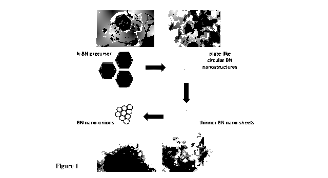
Without wishing to be limited by theory, it is believed the formation of such
nano-onion
structures is driven by the non-coherent light emission from the lamp ablation
which, upon
impinging on the boron nitride precursor material, generates plate-like
circular nanostructures
that exfoliate into thinner boron nitride nano-sheets. Those boron nitride
nano-sheets then
rearrange into a more stable nano-onion structure.
That proposed mechanism for the formation of nano-onion structures according
to the method
of the invention is schematically illustrated in Figure 1. With reference to
Figure 1, h-BN is
used as a precursor material and subjected to lamp ablation. That precursor
material is
believed to initially form plate-like circular boron nitride nanostructures
which exfoliate into
thinner boron nitride nano-sheets. The boron nitride nano-sheets are then
believed to
rearrange into more stable nano-onion structures. As will be discussed below
in more detail in
the examples section, that proposition is supported by experimental evidence
which identified
incompletely-closed nano-onion structures lining exfoliated boron nitride nano-
sheets.
The method according to the invention can advantageously produce a relatively
large
proportion of boron nitride nano-onion structures.
In one embodiment, the nanostructures produced comprise at least 50wt%, or at
least 60wt%,
or at least 70wt%, or at least 80wt%, or at least 90wt%, or at least 95wt%
nano-onion
structures.
As is well known to those skilled in the art, boron nitride nano-onions have a
nano-spherical
structure comprising concentric shells of boron nitride sheets.
The nano-onion structures may be hollow.
In one embodiment, all dimensions of the nanostructures produced are less than
100nm.
CA 03119663 2021-05-12
WO 2020/097688 PCT/AU2019/051256
- 6 -
In a further embodiment, the nanostructures produced comprise nano-onion
structures having
an average diameter ranging from about 15 nm to about 80 nm, or about 20 nm to
about 60
nm.
The nanostructures produced according to the invention may be crystalline.
The nanostructures produced according to the invention have characteristic
features known by
those skilled in the art. For example, the nano-horn structures have a
projection of a hollow
tube where one end is open and the other end is tapered and closed. The
average length of the
nano-horns is typically about 10 nm with an average diameter of about 5 nm.
The average
length of the nano-rods is typically about 15 nm with an average diameter of
about 5 nm. The
nano-sheets typically have a largest average length dimension of about 50 nm.
The method according to the invention comprises subjecting boron nitride
precursor material
to lamp ablation. By being a "precursor material" is meant a boron nitride
source material that
is subjected to lamp ablation so as to form the boron nitride nanostructures.
Those skilled in the art will appreciate that boron nitride exists in varying
polymorphic forms.
For example, it may present in an amorphous form, a hexagonal form, a cubic
form or a
wurtzite form.
There is no particular limitation on the type of boron nitride precursor
material that may be
used in accordance with the invention.
In one embodiment, the boron nitride precursor material subjected to lamp
ablation according
to the invention comprises amorphous boron nitride, hexagonal boron nitride,
cubic boron
nitride, wurtzite boron nitride or a combination of two or more thereof.
In a further embodiment, the boron nitride precursor material subjected to
lamp ablation
comprises hexagonal boron nitride.
CA 03119663 2021-05-12
WO 2020/097688 PCT/AU2019/051256
- 7 -
Typically, the boron nitride precursor material subjected to the lamp ablation
will be in
powdered form.
The boron nitride precursor material subjected to the lamp ablation may itself
comprise or be
in the form of boron nitride nanostructures. Where the boron nitride precursor
material
comprises boron nitride nanostructures, it will be appreciated those
nanostructures (as a
precursor material) will, upon being subjected to lamp ablation according the
invention, be
transformed or converted into different nanostructures. For example, where the
boron nitride
precursor material comprises boron nitride nano-horns, upon being subjected to
lamp ablation
according the invention those nano-horn structures will be transformed or
converted into
different nanostructures, such as nano-onion structures. Accordingly, the
method according to
the invention produces boron nitride nanostructures even when the boron
nitride precursor
material itself comprises boron nitride nanostructures.
In one embodiment, the boron nitride precursor material subjected to lamp
ablation comprises
boron nitride nano-horns, boron nitride nano-rods, boron nitride nano-tubes,
boron nitride
nano-sheets, boron nitride nano-platelets, boron nitride nano-onions or a
combination of two
or more thereof.
The method according to the invention includes subjecting boron nitride
precursor material to
lamp ablation within an adiabatic radiative shielding environment. Without
wishing to be
limited by theory, the adiabatic radiative shielding environment is believed
to be an important
factor in providing for the boron nitride nanostructures.
By the radiative shielding environment being "adiabatic" is meant that
substantially no or
very little heat is lost from the radiative shielding environment. In that
context the
"environment" is intended to mean a space that is defined by the boundaries of
a suitable
radiative shielding material. The radiative shielding material therefore
functions as a highly
efficient insulating barrier to the loss of heat. Those skilled in the art are
well versed in
materials that can provide for such a radiative shielding environment.
Examples of suitable
radiative shielding environment are described herein.
CA 03119663 2021-05-12
WO 2020/097688 PCT/AU2019/051256
- 8 -
The adiabatic radiative shielding environment may be provided in the form of a
vessel.
The vessel may be hermetically sealed and have two or more layers of material
which are each
spaced apart and each hermetically sealed. The hermetically sealed, spaced-
apart, multiple
layers of material create an adiabatic radiative shielding environment.
Without wishing to be
limited by theory, the adiabatic radiative shielding environment is believed
to promote slow
cooling of the ablation products at elevated temperatures, similar to an
annealing heat
treatment. That in turn is believed to enable such unique nanostructures to be
formed.
The adiabatic radiative shielding environment may in part be opaque or
translucent, but it will
of course need to provide a substantially transparent section to the lamp
emission for the boron
nitride precursor material to undergo lamp ablation. For example, the
adiabatic radiative
shielding environment may be in the form of a vessel such as an ampoule, where
at least a
portion of the vessel is transparent to the lamp emission, for example the tip
of the vessel
where the boron nitride precursor material is located. The portion of the
vessel that is
transparent to the lamp emission will typically be located at or proximate to
the focal point of
the lamp.
An example of a adiabatic radiative shielding environment suitable for use in
accordance with
the invention is shown in Figure 3. Figure 3 (a) and (b) illustrate an
adiabatic radiative
shielding environment in the form of an ampoule configuration with
hermetically sealed layers
which are spaced apart. In Figure 3 (a) and (b) (10) points to the boron
nitride precursor
material, (20) points to a hermetically sealed inner layer of used quartz, and
(30) points to a
hermetically sealed outer layer of fused quartz. The portion of the vessel
shown is transparent
to the lamp emission.
In one embodiment, the adiabatic radiative shielding environment is in the
form of a vessel
comprising a section made from fused quartz.
Such fused quartz will be transparent to the lamp emission.
It is preferred the fused quartz used have a high infrared (IR) transmittance.
CA 03119663 2021-05-12
WO 2020/097688 PCT/AU2019/051256
- 9 -
Examples of suitable fused quartz include grades GE214 and GE214A.
The boron nitride precursor material will generally be sealed within an
adiabatic radiative
shielding environment prior to it being subjected to lamp ablation. The
adiabatic radiative
shielding environment will generally be evacuated prior to it being sealed.
For example, the boron nitride precursor material to be subjected to the lamp
ablation may be
located within an adiabatic radiative shielding environment by being sealed
and evacuated in a
quartz glass tube or ampoule.
In one embodiment, lamp ablation of the boron nitride precursor material is
conducted at a
pressure less than atmospheric pressure. For example, that pressure may be
within the range
of about 100 mbar to about lx 10-3 mbar.
It can be desirable to remove any moisture from the boron nitride precursor
material prior to it
being subjected to lamp ablation.
In one embodiment, the boron nitride precursor material subjected to lamp
ablation is
substantially anhydrous.
It can be desirable to subject the boron nitride precursor material to lamp
ablation under an
inert atmosphere.
In one embodiment, the boron nitride precursor material is subjected to lamp
ablation under an
inert atmosphere.
The inert atmosphere may be provided by an inert gas such as nitrogen or
argon.
Depending on how the boron nitride precursor material is physically located
within the
adiabatic radiative shielding environment, it may be necessary to rotate the
boron nitride
precursor material within the lamp emission or rotate the lamp emission around
the boron
CA 03119663 2021-05-12
WO 2020/097688 PCT/AU2019/051256
- 10 -
nitride precursor material, so as to maximise exposure of the precursor
material to the lamp
emission. For example, where the adiabatic radiative shielding environment is
a vessel such
as a tube or ampoule, the tube or ampoule could simply be rotated within the
lamp emission.
In one embodiment, the boron nitride precursor material subjected to lamp
ablation is rotated
within the lamp emission.
In another embodiment, the lamp emission is rotated around the boron nitride
precursor
material.
An important feature of the present invention is the use of lamp ablation to
promote formation
of the boron nitride nanostructures.
Lamp ablation is a technique known in the art and involves subjecting a target
sample to a
high energy non-coherent light source derived from the focussed emission of a
gas-discharge
lamp.
Gas discharge lamps typically comprise one or more noble gases such as argon,
neon, krypton
and xenon. The lamps may further comprise one or more other materials such as
mercury or
sodium. Gas discharge lamps also include so called metal halide lamps.
In one embodiment, the lamp ablation is performed using a xenon lamp, a xenon-
mercury
lamp, a high-pressure mercury lamp, or a metal halide lamp.
Lamps used in lamp ablation emit light energy and that light energy may
conveniently be
referred to as the lamp emission.
Generally, the luminous efficiency of a lamp used to provide for the lamp
emission according
to the present invention will range from about 15 to about 50 lm/W.
Suitable lamp sizes will generally range from about 75 to 10,000 W.
CA 03119663 2021-05-12
WO 2020/097688 PCT/AU2019/051256
- 11 -
In one embodiment, the lamp used for the lamp ablation ranges from about
4,000W to about
10,000W, or from about 6,000W to about 10,000W, or from about 7,000W to about
10,000W.
Generally, the colour temperature of the lamp emission will range from about
5000 to about
6200K.
In one embodiment, the colour temperature of the lamp emission is about
6,000K.
In another embodiment, the boron nitride precursor material is subjected to
lamp ablation at a
temperature in the range between about 1,400 and about 3,500 C.
To perform lamp ablation emission from the lamp is typically reflected off one
or more
surfaces to form a focal point. The boron nitride precursor material may be
placed within the
adiabatic radiative shielding environment which is at or close to that focal
point so as to
promote lamp ablation in accordance with the invention. There will typically
be a temperature
gradient within the adiabatic radiative shielding environment, with the
hottest point generally
being located at or close to the focal point of the lamp, with the remaining
part of the adiabatic
radiative shielding environment progressively becoming cooler moving away from
the focal
point of the lamp.
The boron nitride nanostructures, particularly the nano-onion structures, will
often form within
the adiabatic radiative shielding environment some distance away from the
focal point of the
lamp (i.e. some distance away from the hottest region within the adiabatic
radiative shielding
environment.
In one embodiment, the boron nitride precursor material is located within the
adiabatic
radiative shielding environment which is at or proximate to a focal point of
the lamp ablation
and the boron nitride nanostructures, for example nano-onion structures, form
within the
adiabatic radiative shielding environment at a distance of about 6 cm to about
30 cm, or about
8 cm to about 12 cm, or about 12 cm to about 16 cm, or about 16 cm to about 20
cm, from the
focal point.
CA 03119663 2021-05-12
WO 2020/097688 PCT/AU2019/051256
- 12 -
By the boron nitride precursor material being located "proximate to" a focal
point of the lamp
ablation is meant the material is located within the radiative shielding
environment which
itself is sufficiently close to the focal point for the lamp ablation to
occur. The distance from
the focal point at which the radiative shielding environment containing the
boron nitride
precursor material can be placed to perform the invention can vary depending
on the emission
intensity of the lamp. The key point being that the temperature within the
radiative shielding
environment has to be sufficiently high to provide lamp ablation of the boron
nitride precursor
material located therein. As noted above, the temperature dissipates as one
move away from
the focal point. If the radiative shielding environment containing the boron
nitride precursor
material is not located at the focal point, it will generally be located at no
more than about 2
cm, or 1.5 cm from the focal point.
The present invention can be performed using lamp ablation apparatus known in
the art. For
example, a specular ellipsoidal mirror may be used to reconstitute and focus
the lamp emission
to provide for the lamp ablation apparatus.
An example of a suitable lamp ablation apparatus for use in accordance with
the present
invention is shown in Figure 2. With reference to Figure 2, (a) shows an image
of a lamp
ablation apparatus suitable for use in accordance with the invention, and (b)
represents a
schematic illustration of the highlighted section in (a). Figure 2 (b) shows a
schematic
illustration of a lamp surrounded by an ellipsoidal mirror assembly which
directs the lamp
emission to a focal point. At that focal point is an adiabatic radiative
shielding environment in
the form of a sealed evacuated tube/ampoule containing boron nitride precursor
material being
subjected to lamp ablation according to the invention.
As previously discussed, when performing lamp ablation in accordance with the
invention it
will be desirable to maximise exposure of the boron nitride precursor material
to the lamp
emission. That may be achieved by rotating the boron nitride precursor
material within the
lamp emission. For example, that can be achieved by rotating the ampoule/tube
shown in
Figure 2(b). Alternatively, the lamp ablation apparatus may be rotated around
the boron
nitride precursor material.
CA 03119663 2021-05-12
WO 2020/097688 PCT/AU2019/051256
- 13 -
The time of exposure of the boron nitride precursor material to lamp ablation
will vary
depending upon factors such as the amount of boron nitride precursor material
and the type of
lamp ablation apparatus used. Those skilled in the art can readily determine a
suitable time for
subjecting the boron nitride precursor material to lamp ablation based on the
specific
equipment and conditions being used.
In one embodiment, the boron nitride precursor material is subjected to lamp
ablation for at
least 5 minutes, or at least 10 minutes, or at least 15 minutes, or at least
20 minutes, or at least
30 minutes, or at least 40 minutes, or at least 50 minutes, or at least 60
minutes.
If desired, the boron nitride precursor material may be subjected to multiple
lamp ablation
exposures. In other words, lamp ablation may be performed on the boron nitride
precursor
material multiple times.
There is no particular limitation on applications for the boron nitride
nanostructures produced
in accordance with the method of the invention. As the method of the invention
is particularly
well suited for producing boron nitride nano-onion structures, the product
produced by the
method can advantageously be used as a dry/solid lubricant. The nanostructures
produced in
accordance with the method of the invention may also be used in providing for
anti-wear
materials.
The following invention will hereinafter be described with reference to the
following non-
limiting examples.
Examples
Apparatus
Lamp ablation was performed using apparatus as shown in Figure 2. A large
specular
ellipsoidal mirror reconstitutes the power density of the lamp derived plasma
inside a
nominally 7 kW continuous ultra-bright Xenon short-arc discharge lamp at a
focal point.
The peak irradiance in the focal region was -6 W/mm2 on an area of -300 mm2, a
s estimated
CA 03119663 2021-05-12
WO 2020/097688 PCT/AU2019/051256
- 14 -
by conjoining manufacturer lamp radiance data with raytrace simulation
results.
General procedure
The boron nitride precursor powder used was analytical grade h-BN, sealed in
evacuated
quartz ampoules consisting of two layers of fused quartz, each hermetically
sealed. The
irradiated ampoules were rotated by -180 every 60 seconds to ensure that as
much of the
precursor powder as possible was directly irradiated. In separate experiments,
continuous lamp
ablation was conducted for 30 and 50 minutes.
The ampoules were subsequently cut into several sections, each of which was
analysed
separately. The ablated products were mixed with high-purity ethanol, and the
solution was
used to prepare samples that were analysed in a Transmission Electron
Microscope (FEI Titan
G2 80-200 TEM/STEM, JEOL 2100 TEM) and Scanning Electron Microscope (Verios
XHR
SEM).
Results and Discussion
To distinguish product nanostructures from the BN precursor material, TEM and
SEM images
of the h-BN precursor powder (Figs. 4 (a) and (b), respectively) were first
generated. Those
images confirm the distinct hexagonal shape and high purity of the precursor.
Figure 4 (c)
shows the X-ray diffraction (XRD) pattern, where the four peaks at d-spacings
of 3.32805,
2.16692, 2.06206, 1.81562, 1.66521 A can be indexed as h-BN for the planes
(002), (100),
(101), (102) and (004), respectively. The lattice constants are a = 2.502 and
c = 6.656 A,
which are close to the literature values a = 2.5044 and c = 6.6562 (JCPDS card
no. 34-421).
Nano-pellets were found nearer to the lamp's focal point compared to the nano-
onions
described below and would appear to be an intermediate stage in the
transformation of the
precursor BN material to the final nanostructures. The fact that the
nanostructures primarily
comprise boron and nitrogen is evidenced by the energy-dispersive x-ray
spectroscopy (EDS)
spectrum (Fig 5).
CA 03119663 2021-05-12
WO 2020/097688 PCT/AU2019/051256
- 15 -
The section of the quartz ampoule approximately 12-16 cm from the lamp focus
revealed
remarkable clusters of hollow BN nanospheres (nano-onions) with diameters of
50-100 nm.
Results from the 30-minute ablation experiment exhibited no noticeable
differences relative to
the 50-minute exposure, including the observation that the BN nano-onions were
found
principally at a similar distance (12-16 cm) from the focal region. The
diameters of the
structures range from 20-60 nm. The applied difference in irradiation time had
no
perceptible effect on the size or shape of the nano-onions. The fact that the
nano-onions
primarily comprise boron and nitrogen is evidenced by the energy-dispersive x-
ray
spectroscopy (EDS) spectrum (Fig. 6). The appearance of carbon and copper in
the EDS
spectrum (Fig. 6) can be explained as background from the copper TEM grid
having a porous
carbon film. The presence of silicon and oxygen is due to tiny quartz shards
produced from
cutting the ampoule during sample preparation.
Figure 7 (a) illustrates the profile taken along the wall of a BN nano-onion.
The FFT (not
shown), together with the line profile, is used to estimate an inter-layer
spacing of 0.335 nm,
which accords well with the established (002) lattice spacing of h-BN. Figure
7 (b) shows
the line profile taken through a single nano-onion. The variation in counts in
the profile is
closely related to the relative thickness, reinforcing that the nano-onions
are in fact hollow.
Electron energy loss spectroscopy (EELS) analysis of the BN nano-onions shows
the distinct
absorption peaks of B and N: characteristic K-shell ionisation edges at 188
and 401 eV,
respectively. The sharp 7C* and a* peaks of the B and N K-edges are
characteristic of the
sp2 bonding configuration, underscoring the h-BN structure. The carbon
absorption peak at
284 eV can be attributed to the carbon film on the TEM copper grid.
A quantitative analysis of the spectrum shows a B/N atomic ratio of 1.00
0.02. In the
EELS spectrum, the change in the relative intensities of the 7C* and a* peaks
between the
wall and the centre of the nano-onions (Figs. 8 (a) and (b)) are due to the
orientation-
sensitive nature of sp2-hybridised BN in the EELS microanalysis.
CA 03119663 2021-05-12
WO 2020/097688 PCT/AU2019/051256
- 16 -
A variety of other BN nanostructures were discovered in the same region of the
ampoule,
mainly nano-platelets and exfoliated nano-sheets. The nano-platelets are two-
dimensional,
with diameters of approximately 50 nm. Numerous nano-onion structures that did
not fully
close were found around the edges of the exfoliated sheets.
More subtle nanostructures, such as nano-horns and nano-rods were also
observed.
Furthermore, nano-rod and concentric tubular nanostructures were found.
The elements present in both the nano-platelets and nano-sheets are clear from
the EDS
spectrum in Figure 9, dominated by B and N. The presence of Si and 0 can be
attributed
to shards from the cut quartz reactor ampoules (vide supra), and the presence
of C is due to
the carbon film on the copper TEM grid.
Without wishing to be limited by theory, a formation mechanism for such
nanostructures that
is not inconsistent with the experimental observations (Fig. 1) is that
exfoliated and
vaporised h-BN condenses into a variety of structures, which change their
morphology to
form the lower-energy hollow nano-onions. The h-BN precursor could initially
form plate-
like circular nanostructures of BN which exfoliate into thinner sheets of BN
and could then
rearrange into more stable nano-onions at a cooler section of the vessel some
distance away
from the focal point of the lamp. The photo-thermal transformation is driven
by the adiabatic
radiative shielding environment within the vessel that permits slow cooling of
the ablated
material. The supporting evidence is based on the numerous incompletely-closed
nano-
onions found lining the exfoliated sheets that both the plate-like
nanostructures, as well as
the exfoliated sheets, have dimensions comparable to the nano-onions.
Throughout this specification and the claims which follow, unless the context
requires
otherwise, the word "comprise", and variations such as "comprises" and
"comprising", will be
understood to imply the inclusion of a stated integer or step or group of
integers or steps but
CA 03119663 2021-05-12
WO 2020/097688 PCT/AU2019/051256
- 17 -
not the exclusion of any other integer or step or group of integers or steps.
The reference in this specification to any prior publication (or information
derived from it), or
to any matter which is known, is not, and should not be taken as an
acknowledgment or
admission or any form of suggestion that that prior publication (or
information derived from
it) or known matter forms part of the common general knowledge in the field of
endeavour to
which this specification relates.