Note: Descriptions are shown in the official language in which they were submitted.
CA 03119854 2021-05-13
WO 2020/097732 PCT/CA2019/051625
HIGH RESOLUTION MULTIPLEXING SYSTEM
The invention pertains to a method and device for measuring time varying
particle fluxes
with improved temporal resolution and improved signal to noise ratio. The
particles can be
photons, neutrons, electrons and electrically charged particles.
BACKGROUND OF THE INVENTION
The amplitude of particle fluxes is conventionally measured by collecting the
particle
flux, directing the particle flux onto a transducer that produces an
electrical signal (voltage or
current) with amplitude proportional to the particle flux, conditioning the
electric signal, and
comparing the electric signal with a set of standard electric signals to
assign a numeric value to
the particle flux amplitude. The last step is conventionally done with analog
to digital converters
(ADC).
Analog to digital converters act as an interface between analog electric
signals and a
digital computation device for applications that range from instrumentation,
to radar to
communications. Two main criteria are used to specify the performance of an
ADC, the
sampling rate expressed in Hz and the precision. The precision of an ADC is
variously expressed
in dB or effective number of bits (ENOB). Generally, the precision of an ADC
declines as the
sampling rate increases and hence the precision of the particle flux
measurement also declines.
One general object of the invention is to increase the precision of particle
flux measurements at
high sampling rates. A further major goal of the invention is to increase the
maximum sampling
rate achievable so that changes in particle flux over a short temporal
interval can be resolved.
In prior art, high frequency ADC's (>1 GHz) typically consist of a stack of
two or more
lower rate ADC's that are temporally interleaved to achieve precision close to
that of the lower
rate ADC. These designs rely on timing circuits to route the input signal to
each ADC in the
stack in sequence. An error is introduced because there is jitter in the
timing signals. A goal of
the present invention is to reduce the error caused by jitter in the timing
signals. Further errors
are introduced variability between interleaved ADC's in a stack, specifically,
there are offset
and gain error. A goal of the invention is to reduce effects of gain and
offset errors.
CA 03119854 2021-05-13
WO 2020/097732 PCT/CA2019/051625
2
The invention can be used in applications such as radar, communications and
instrumentation that require both a high data rate and high precision and
accuracy. An
exemplary application of the invention is a multi-gigahertz signal analyzer,
henceforth GSA.
The exemplary GSA takes optical Or electronic signals as input. The GSA is
illustrative of the
concepts of the invention and does not limit the scope of the invention.
SUMMARY OF THE INVENTION
The invention provides a multiplex method for measuring the temporal
dependence of a
particle flux. The particles can be electrons, ions, neutrons or photons. In
the context of the
to following discussion, the term flux refers to either the number of
particles per unit time or the
energy carried by said particles per unit time crossing a plane normal to the
direction of motion.
The invention is a system comprising a set of electronic and/or optical
components and
a set of algorithms that implement N-fold temporal multiplexing of the input
flux. The input
flux may be electrons or photons or ions or neutrons. The system can be used
to measure other
types of flux by using a transducer to convert the flux into a compatible
form. For example the
system can include a transducer such as a scintillator that operates to
convert particle flux
incident into a photon flux proportional to the amplitude of particle flux.
The invention can be
used with multiplexing methods known to those skilled in the art, for example
Hadamard and
Fourier methods.
Preferably but not necessarily the invention is used with high efficiency
multiplexing
(HEMS) described in US Application 15/987,279 filed May 23, 2018 by the
present Applicant,
which corresponds to PCT Application PCT/CA2018/050599 published on 29
November 2018
as WO 2018/213923 the disclosure of which is incorporated herein by reference.
HEMS is a
method to improve the signal to noise ratio (SNR) of particle flux
measurements. The
description below includes some references to HEMS and it will be appreciated
that these are
merely exemplary and the invention herein can be used with other methods.
The input flux c1:0 is connected to a signal conditioning device. The signal
conditioning
device may have no effect or the signal conditioning device may be an
amplifier or the signal
conditioning device may add the input flux to another flux. The output from
the signal
conditioning device is divided into N substantially equal parts and each part
each with flux 4o =
CA 03119854 2021-05-13
WO 2020/097732 PCT/CA2019/051625
3
cD/N is directed along a different path to a different gate device. Each gate
device is connected
to at least one integrating device. In HEMS embodiments there are d
integrating devices, where
d is an integer greater than 1. The gate device functions to either block the
flux 4), or to direct
all of the flux to one of d integrating devices based on a pre-set code
sequence of length N. The
integrating device functions to produce an electric signal proportional to the
integrated flux it
receives from the gate device. Each element in the code sequence identifies
the action to be
taken by the gate device for time interval T. Preferably the time intervals
are equal and the total
integration time is T = N. The arrangement herein will work with unequal time
intervals in
which case the total integration time is T = Iti. At the end of each
integration period T, each
to integrating device transfers an electric signal proportional to the
integrated flux to either an
optional buffering device or directly to an ADC of conventional design. The
buffering device
stores the electric signal from the integrating device substantially unchanged
for a period at least
21 and preferably longer than NT. The integrated signals stored in the
buffering devices are
optionally processed with analog circuits to produce an analog quantify a,
proportional to the
average flux (A during each time interval
Optionally the analog quantity a, is compared with an analog threshold value
to produce
information about the incident flux.
Optionally, and possibly on the basis of the optional analog comparison, the
analog
quantity a, is transferred to a conventional ADC and converted into digital
form.
Optionally, the set of Nd integrated signals in the buffer devices are
transferred to one
or more ADC's of conventional design and converted to digital values. The
digital values are
then processed with a digital processing device to provide numbers
proportional to the average
flux 4:13, during each time interval ti.
The integrators are any device known in the art that sum a signal. The
integrator may
be, for example a capacitor. The buffers are any device known in the art that
stores a signal
substantially unchanged. The buffer may be, for example a capacitor that
stores electric charge.
The gates are any device known in the art that switches a signal from one path
to two or more
alternate paths. The term "signal" here refers to an analog quantity such as a
quantity of
electrons or a voltage. Preferably the input signal and switched signal are
related by a constant
of proportionality. Ideally the constant of proportionality is one. The gate
may be for example
an electronic MUX. The temporal response of a standard MUX in prior art may be
insufficient
CA 03119854 2021-05-13
WO 2020/097732
PCT/CA2019/051625
4
for some high frequency applications of the present invention. In some
embodiments, the
arrangement herein includes delay lines as described further below to achieve
temporal
resolution for the ADC system as a whole better than the temporal resolution
of the gate
elements. In some embodiments, the invention includes an electro optical
switching mechanism
as described in further detail below to achieve temporal resolution better
than the temporal
resolution of the gate elements.
In one embodiment the arrangement provides the following steps:
collecting the incident particle flux in each time interval;
directing the particle flux into a conditioning device that outputs N
conditioned particle
fluxes with amplitude proportional to the incident particle flux along N
different paths to a gating
device on each said N paths;
each said gating device operating to direct particle flux along one of at
least two different
gated paths at each time interval according to a code sequence unique to each
said gating device;
directing the particle flux along each of the gated path to a respective
integrating device;
(however one of the two paths may be a dead end so that in this case only one
of the paths is
integrated)
each said d integrating devices operating to produce an electrical signal
proportional to
the integrated particle flux over N time intervals;
and analyzing said Nd electrical signals to obtain information about the
amplitude of the
incident particle flux over N time intervals;
wherein each unique code sequence is of length N and has at least two
different elements
specifying at least two different gated paths and d is greater than or equal
to one.
That is when d = 1 one path is a dead end and is not used.
Optionally the steps include directing each electrical signal to a buffering
device that
operates to store said electrical signal.
In one arrangement where the analysis is carried out by ADC, the steps
include:
directing each said electrical signal to an analog to digital converter that
operates to
produce a digital value proportional to the electrical signal;
and directing said Nd digital values to a digital computing device.
CA 03119854 2021-05-13
WO 2020/097732
PCT/CA2019/051625
In another embodiment where analysis is carried out by ADC to produce time
sequence d=1 case, the steps include:
directing each said electrical signal to an analog to digital converter that
operates to
produce a digital value proportional to the electrical signal;
5 directing said N digital values to a digital computing device;
arranging said N digital values into a data vector Y;
and multiplying said data vector Y by a matrix H to obtain information about
the
amplitude of the incident particle flux over N time intervals;
where d is equal to one, the matrix H is the inverse of a matrix Z, Z has N
rows of length
N, each corresponding to one gating device and each row of Z is the unique
code sequence for
one gating device.
In another embodiment where analysis is carried out by ADC to produce time
sequence Hadamard case, the steps include:
directing each said electrical signal to an analog to digital converter that
operates to
produce a digital value proportional to the electrical signal;
directing said N digital values to a digital computing device;
arranging said N digital values into a data vector Y;
and multiplying said data vector Y by a matrix H to obtain information about
the
amplitude of the incident particle flux over N time intervals;
where d is equal to one, the matrix H is the inverse of a matrix Z, Z has N
rows of length
N, each corresponding to one gating device and each row of Z is the unique
code sequence for
one gating device and each row of Z is the unique code sequence for one gating
device wherein
the unique code sequences are cyclic permutations of a Hadamard sequence.
In another embodiment where analysis is carried out by ADC to produce time
sequence HEMS case, the steps include:
directing each said electrical signal to an analog to digital converter that
operates to
produce a digital value proportional to the electrical signal;
directing said Nd digital values to a digital computing device;
arranging said Nd digital values into a data vector Y;
CA 03119854 2021-05-13
WO 2020/097732 PCT/CA2019/051625
6
and multiplying said data vector Y by a matrix H to obtain information about
the
amplitude of the incident particle flux over N time intervals;
where d is greater than one, and the matrix H is (ZTZ)-IZT, Z has dN rows, and
each row
of Z is the unique code sequence for one gating device wherein the unique code
sequences are
pseudo random sequences.
In another embodiment where analysis is carried out in hardware general case,
the steps include:
directing each said electrical signal to a hardware processor that operates to
produce
to combinations of said electrical signals;
and comparing at least one said combination with a threshold electrical signal
value to
obtain information.
In another embodiment where analysis is carried out in hardware PCA case, the
steps include:
directing each said electrical signal to a hardware processor that operates to
produce
projections of said electrical signals onto at least one principle component;
and comparing at least one said projection onto a principle component with a
threshold
electrical signal value to obtain information about the input.
In another embodiment where analysis is carried out in hardware general case
with ADC follow-up, the steps include:
directing each said electrical signal to a hardware processor that operates to
produce
combinations of said electrical signals;
comparing at least one said combination with a threshold electrical signal
value to obtain
information;
based at least in part on said information, directing at least one said
electrical signal to
an analog to digital converter for conversion into a digital value;
and analyzing at least one digital value to obtain information about the input
signal.
CA 03119854 2021-05-13
WO 2020/097732 PCT/CA2019/051625
7
In another embodiment where analysis is carried out in hardware general case,
with ADC follow up to time sequence. the steps include:
directing each said electrical signal to a hardware processor that operates to
produce
combinations of said electrical signals;
and comparing at least one said combination with a threshold electrical signal
value to
obtain information;
and based at least in part on said information, directing N electrical
signals;
directing each said electrical signal to an analog to digital converter that
operates to
produce a digital value proportional to the electrical signal;
directing said Nd digital values to a digital computing device;
arranging said Nd digital values into a data vector Y;
and multiplying said data vector Y by a matrix H to obtain information about
the
amplitude of the incident particle flux over N time intervals;
where d is equal to one, the matrix H is the inverse of a matrix Z, Z has N
rows of length
N, each corresponding to one gating device, each row of Z is the unique code
sequence for one
gating device wherein the unique code sequences are cyclic permutations of a
Hadamard
sequence.
In another embodiment where analysis is carried out in hardware general case
with ADC follow up to time sequence, the steps include:
directing each said electrical signal to a hardware processor that operates to
produce
combinations of said electrical signals; =
and comparing at least one said combination with a threshold electrical signal
value to
obtain information;
and based at least in part on said information, directing at least one said
electrical signal
directing each said electrical signal to an analog to digital converter that
operates to
produce a digital value proportional to the electrical signal;
directing said Nd digital values to a digital computing device;
arranging said Nd digital values into a data vector Y;
and multiplying said data vector Y by a matrix H to obtain information about
the
amplitude of the incident particle flux over N time intervals;
CA 03119854 2021-05-13
WO 2020/097732 PCT/CA2019/051625
8
where d is greater than one, the matrix H is (ZTZ)-IZT, Z has dN rows, and
each row of
Z is the unique code sequence for one gating device wherein the unique code
sequences are
pseudo random sequences.
In some embodiments the signal conditioning device includes a component to
detect the
start of a periodic signal sequence and which produces a start signal. The
start signal in turn
causes each gate device to begin its coded sequence at a constant time delay
relative to said start
signal. For example the start detection component can be a comparator.
Further, the embodiment
may include a delay path from the signal source to the gate devices so that
the start signal arrives
at the gate devices before the signal to be measured.
The code sequence of length N for each gate device includes at least two
distinct values.
That is, for at least one interval in the set of N intervals, the gate device
delivers flux (I) to
destination different from the destination in the first interval. Preferably,
the code sequence
assigns approximately the same number of intervals to each destination. In
some embodiments
the code sequence is a Hadamard sequence. In some embodiments the code
sequence is pseudo-
random. Each code element specifies which integrating device (or no
integrating device) to use
for one interval T. For example, if d=4 and the code element is 3, the flux is
directed to the 3rd
integrating device.
In an important embodiment, each gate device is connected with two or more
sets of
integrating devices and the code sequence operates on only one set for each
integration period
T. This feature is useful because practical integrating devices such as
capacitors require a period
to reset. In this embodiment, one set is integrating while the other sets are
transferring integrated
signal and resetting to zero.
In some embodiments, the signal conditioning device splits the incident flux
43:1 into two
equal parts. One part is unaltered. The second part is inverted and sent on a
path that introduces
a delay T. The second part is recombined with the first part, and the combined
flux is divided
into N parts and directed along paths to N gate devices as described above. In
this embodiment,
each integrating device contains the integrated signal over the previous N
intervals. That is for
each signal added, the same signal is subtracted a period T later. This
embodiment eliminates
the latency T as a new set of integrated signals is available after each
interval T.
In some embodiments, there is one integrating device connected with each gate
device
and the possible states of the code sequence are either connected to the
integrator or
CA 03119854 2021-05-13
WO 2020/097732
PCT/CA2019/051625
9
unconnected. This embodiment has the same overall throughput as prior are
interleaved
systems, but adds the multiplex advantage to improve the SNR.
In some embodiments, d = 1 and the code sequence is a Hadamard sequence. In
this embodiment
Y = ZB + (1)
where Y is a vector of measured parameters, B is a vector describing the
particle flux 0
in which each successive row of B corresponds to the average flux during
successive period -c,
and Z is a matrix of coefficients describing how much of the particle flux
from each value of the
flux field goes into each measurement of observed parameters Y and E is the
error. If the
integration intervals T are unequal, the coefficients of the Z matrix are
weighted by the actual
values to compensate. Equation 1 has solution
B = el( (2)
The Hadamard embodiment makes the same number of measurements as the
sequential
interleaved scheme in prior art systems, but errors due timing jitter are
reduced because average
values over a period t are calculated rather than the instantaneous value at
an instant. Further,
the multiplex method reduces uncorrelated noise generated in the electronics
in proportion to N-
ta. Noise entering the signal before the input stage of the invention is
faithfully reproduced for
single event. If the signal is recurring, the multiplex method will also
reduce uncorrelated noise
entering the signal before the input stage.
In a preferred embodiment, d> 1 and code sequences are cyclic permutations of
a
pseudo-random sequence chosen to minimize measurement error. As discussed in
the HEMS
application, equation 1 in this case has the least squares solution:
B (ez)izTy (3)
H = (ZTZ)-IZT (4)
All of the comments about noise reduction in the Hadamard embodiment above
also
apply to this embodiment, except that the magnitude of the SNR is greater and
hence this
embodiment is preferred. This embodiment requires d times the sample
throughput of prior art
high rate ADC systems. The advantage of this embodiment is that the signal to
noise ratio (SNR)
CA 03119854 2021-05-13
WO 2020/097732 PCT/CA2019/051625
is higher and consequently higher bit depth for equivalent sampling rate is
achievable. Other
statistical methods can be used. Those skilled in the art will recognize that
equations 2 and 3
apply to cases where the uncertainties in measured values are equal and that
alternative forms
have been derived for cases where the uncertainties are unequal. Other methods
such as neural
5 networks can be used, and are particularly useful in cases where the
uncertainties in measured
parameters Y are unequal.
In some d> 1 embodiments, the flux (1) is divided unequally between paths and
the
integrated signals along each path are multiplied by a calibration constant
such that the sum of
integrated signal over all integrating devices d on a path multiplied by said
calibration constant
10 is the same for all N paths.
In some embodiments, the analog values of Y are delivered to a conventional
ADC,
digitized, and the time sequence B = HY is calculated by the digital
processing device.
In some embodiments, the analog values of Y are delivered to a conventional
ADC,
digitized with a first bit resolution and the digital representation of Y is
analyzed by a digital
processing device to obtain first information and based at least in part on
said first information,
a decision is made whether or not to process the same analog values of Y with
an ADC of
conventional design with second bit resolution. This embodiment is useful for
applications
where the data of interest is sparse. For example, a radar application might
process all of the Y
vectors with a fast 8 bit ADC and based on the result of analysis, deliver
some of the V vectors
from buffering devices to a slower 24 bit ADC in order to analyze signals of
interest at higher
resolution.
In some embodiments, the matrix multiplication HY is performed by analog
circuits and
the result is stored in buffer devices in analog form.
In some embodiments the analog values of B are compared with threshold analog
values
and an action is taken based at least in part on the result of the comparison.
In some embodiments, the linear combinations of the analog values of Y are
calculated
by analog circuits and at least one of the linear combinations is compared
with at least one
threshold value and an action is taken at least in part based on the result of
the comparison. This
feature is useful for pattern recognition by for example Principle Component
Analysis (PCA).
In this example, the projections onto the principle components are linear
combinations of the Y
data vector. Note that the same result is found if B is calculated first,
albeit with more
CA 03119854 2021-05-13
WO 2020/097732 PCT/CA2019/051625
11
computation required. In a radar application the analog comparison could be
used to sort signals
of interest from background noise and then to digitize only the signals of
interest.
In some embodiments, Nd integrated analog signals from each integration period
are
buffered and only one conventional ADC processes all Nd analog values read
sequentially from
buffer devices. Those skilled in the art will recognize that the offset and
gain errors disappear
within blocks of N flux values corresponding to one sampling period T. Of
course, additional
ADC's will be required to process blocks acquired during the time it takes one
ADC to process
Nd samples and there will be offset and gain errors between blocks handled by
different ADC's.
The advantage of this embodiment is that the errors are just level shifts at
predictable intervals
to .. T and easily corrected in the digital domain.
In some embodiments, an array of buffer devices is connected with at least two
types of
ADC elements A and B. A type A ADC is capable of operating at rate f/N
outputting a digitized
result with bit depth ba. A type B ADC operates at a lower rate than f/N, but
outputs a digitized
result with bit depth bb>ba. For an example, in a hypothetical 4 GHz system
with 500 MHz
ADC's, type A is a 500 MHz ADC that outputs an 8 bit result and type B as a 4
MHz ADC that
outputs a 24 bit result. In operation, the system functions as follows. The
type A ADC's
digitizes all of the samples in the sample space and hardware or software
processors separates
the time series into regions with background and regions with a feature of
interest. The buffers
corresponding to the feature of interest are read by the type B ADC and the
higher resolution
results are analyzed to obtain information about the feature of interest.
In some applications, the desired temporal resolution 8 is less than the gate
switching
time T of the hardware employed. Let p = T/8 be the ratio between the minimum
gate switching
time and the desired temporal resolution. Further, p is rounded to the nearest
integer. For
example, if the minimum switching time for a MUX is 5 ns and the required 6 is
50 ps, then p
=100. The gate switching time is not a limiting factor per se because the gate
function merely
convolutes the higher resolution signal. Since the gate function is known, the
higher resolution
signal can be recovered by deconvolution. The ultimate temporal resolution
does not depend on
the gate period, but rather the smallest possible offset to the start of the
gate period. The offset
to the start of a gate period can be generated in a FPGA, for example.
Alternately the length of
control lines to the gate device can be of different lengths so that control
signals propagating
along longer lines arrive later. If the path for an electron traveling at c/3
is changed by 1 micron,
CA 03119854 2021-05-13
WO 2020/097732 PCT/CA2019/051625
12
the difference in time of arrival is 10 fs. Although the increments in the
delay line are preferably
of equal length, it is not necessary. All that is required is that the
increments differ from one
another by approximate integer multiples of S and that their lengths are
known. To elaborate,
the present method finds the average flux during the actual time intervals of
the integration and
it is understood that the calculated result has uneven time intervals that
reflect the measurement
time intervals. A result with equal time intervals can be obtained by
interpolation. For
illustrative purposes, two methods using deconvolution are outlined below.
The first mathematical approach is to model the measurement as a set of p time
series of
total length T offset one from the next by S. Each time series is determined
separately as Bn =
to HYn ,where n runs from 1 to p. In this case H has N rows. The resolution
of each time series
is limited to T by the gate. The p time series of length N are interleaved to
give a combined
series of length pN with point spacing 5. The resulting time series is a
convolution of the signal
with the gate period z. Since T, and presumably the shape of T is known, the
signal can be
recovered by standard deconvolution methods known to those skilled in the art,
for example
Fourier deconvolution.
The second mathematical approach is to model the system like the Toeplitz case
discussed in the HEMS application. In this case, the dimension of Z is
increased by a factor of
p. In a preferred embodiment Z contains at least two block sizes s and t of
different length that
don't have a common divisor. Further, s and t are integers greater than or
equal to the minimum
block size p. Preferably s and t are also prime numbers. In most preferred
embodiments there
are more than two block lengths and the lengths are prime numbers. The number
of choices for
the multiplexing sequence Z is very large with some choices giving a better
signal-to-noise ratio
(SNR) than other choices.
For a static spatial mask, in the Toeplitz case, the matrix (ZTZ)-1 is
singular and hence
the transform matrix H = (ZTZ)-1 ZT is not valid. However, the convolution due
to motion of a
spatial mask during measurement renders (ZTZ)-1 non-singular and data points
at a higher
nominal resolution can be calculated as discussed in the HEMS application. The
achievable
signal to noise ratio (SNR) depends on the details of the convolution.
Likewise, the finite
transition time of the gate produces a temporal convolution that renders
(ZTZyl non-singular.
Specifically, there is some division of flux to different integrators during
the switching time that
provides the needed convolution. The signal is calculated directly as B = HY.
Hence, by
CA 03119854 2021-05-13
WO 2020/097732 PCT/CA2019/051625
13
methods previously described for spatial resolution, it is possible to achieve
finer temporal
resolution than the width of a modulator element, albeit with some degradation
in the SNR.
In some embodiments, the incident flux eD is split into Np equal parts; each
part is
directed to a gate, each gate device directs flux to an integrating device
specified by a code
sequence of length Np; the integrating devices integrate the signals; and the
integrated signals
are analyzed to determine the temporal dependence of the input flux wherein
the code sequence
consists of sub sequences of length greater than or equal to p. This
embodiment corresponds to
the Toeplitz case described in the HEMS application.
In some embodiments the gate device is comprised of one or more electro-
optical devices
that divert incident photon flux into different integrating devices in
response to control signals.
In a preferred embodiment two sequential electro-optical devices divert
incident photon flux
into integrating devices arranged along a closed path wherein the integrating
devices are shaped
to implement a code sequence. Preferably the integrating devices integrate
photo-electrons
produced by the photo-electric effect when the photon flux is incident on said
integrating device.
In some embodiments the gate device is comprised of one or more electric
deflection
devices that divert incident electron flux into different integrating devices
in response to control
signals. In a preferred embodiment two sequential electric deflection devices
divert incident
electron flux into integrating devices arranged along a closed path wherein
the integrating
.. devices are shaped to implement a code sequence.
BRIEF DESCRIPTION OF THE DRAWINGS
Figure 1 is a schematic, of a PRIOR ART high rate interleaving ADC operating
at
frequency f samples per second.
Figure IA is an illustration of the signals of the ADC of Figure 1 including
the input
signal 303 and a series of clock signals.
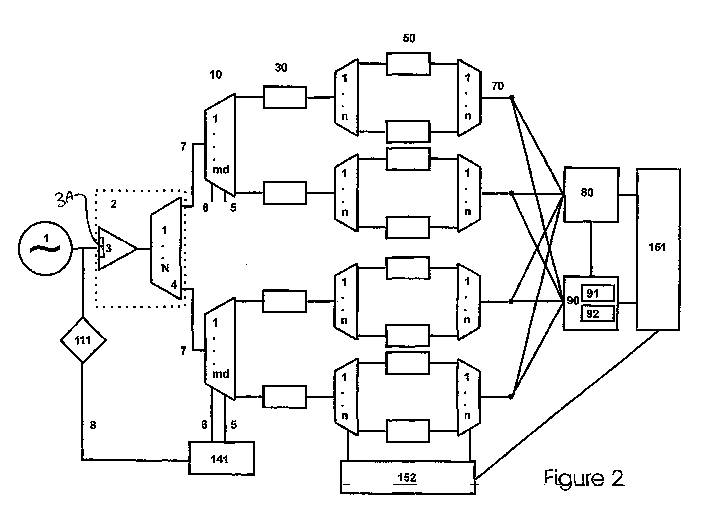
Figure 2 shows a preferred embodiment of the present invention.
Figure 3 shows a schematic view of a multiplex integration unit for use in the
embodiment of Figure 2 using seven gate devices.
Figure 4 shows a series of example waveforms including time shifted signals
generated
by delay lines to shift the start of an integration interval by less than a
clock period.
CA 03119854 2021-05-13
WO 2020/097732 PCT/CA2019/051625
14
Figure 5A shows a schematic for a fast switching method.
Figure 5B shows integrating devices are arranged around the ring of Figure 5A.
DETAILED DESCRIPTION
Figure 1 shows a schematic view of a high speed analog to digital conversion
system
according to prior art. Analog input 1 is amplified 2 and the resulting analog
signal 303 is
transmitted to switch 11 connected to timing control 141. Each clock cycle at
frequency f,
timing control 141 increments the address of the ADC in stack to connect with
the analog cycle
and resets to the first address after the last address is connected. In the
example shown, the
ADC's in the stack are connected in the repeating sequence 81, 82, 83, 84. The
clock input is
indicated as 304 and the waveforms for ADC's 81, 82, 83, and 84 are indicated
as 121, 122, 123
and 124, respectively. The value of the input signal 303 is captured on the
rising edge of the
timing pulse for each ADC. That is ADC's 81, 82, 83 and 84 read the signal at
the indicated
instants 221, 221, 223, and 224, respectively. Each ADC in the stack outputs a
digital result at
frequency f/N (f/4 in the example shown) to interleaver 121, which passes an
ordered sequence
of digital values to computation device 151. Computation device 151 processes
the raw stack
ADC outputs to reduce the effects of offset, gain and timing errors. There is
a one-to-one
relationship between each sample interval and a corresponding ADC.
Figure 2 shows a general schematic of the invention. Particle flux is
collected and enters
the system at 1 as an analog signal. The analog signal enters conditioning
device 2 that includes
amplifier 3 and splitting device 4. The conditioning device 2 can also include
a filter 3A which
operates to reject at least a part of the input particle flux amplitude.
Splitting device 4 and
amplifier 3 work together so as to produce N clones of analog signal 1 with
amplitude (or
equivalently particle flux) at each instant in time proportional to the
amplitude of analog signal
1. The N cloned analog signals denoted 7, are directed to N gate devices
generally indicated as
the column 10. The paths 7 are arranged in a manner such that the signal
arriving at each gating
device is in phase with the signal at all of the other gates. The operation of
gate devices 10 is
coordinated by timing control 141 which directs timing signals 5 and control
signals 6 to each
gate device 10. Optionally, the input signal 1 is compared with a threshold
111 and if a threshold
condition is met a signal 8 is transmitted to timing control 141. The signal
lines are arranged
such that the propagation delay for the cloned signals 7 is greater than or
equal to the propagation
CA 03119854 2021-05-13
WO 2020/097732 PCT/CA2019/051625
delay for the threshold signal 8 plus the timing and control signals 5 and 6.
The threshold
comparison 111 can be used, for example to detect the start of a transient
signal and to
synchronize subsequent data acquisition. This enables the arrangement herein
to compare the
input signal with a reference signal relative to the same threshold. The gate
devices 10 select
5 one of md paths in accordance with a code sequence and direct the cloned
signal 7 along said
selected path to an integrating device generally indicated in column 30. The
integrating devices
integrate the cloned signal incident for N integration intervals.
As better shown in Figure 3, the cloned waveform 303 on signal line 7 is
incident on
gate device 11 which directs the waveform to either integrating device 31 or
integrating device
10 32 in accordance with a code sequence. In the example shown in Figure 3,
N=7 and d=2. Gating
devices 11, 13, 15, 17, 19, 21 and 23 along with two associated integrating
devices with sample
control waveforms are shown. Each gating device nominally receives the same
input signal 7
and consequently the sum over each set of md integrating devices for N
integration intervals
should be the same. However due to small differences in component parts, the
sums may vary.
15 The variance can be corrected in digital processor 151 by summing each
set and then dividing
each value of the set by the sum as discussed in the HEMS application
referenced above. In
contrast to the prior art, there is a one-to-N relationship between time
interval and integrators.
In this example, the waveforms are cyclic permutations of a Hadamard sequence
of length 7 and
the compliment of each. The waveforms for integrating devices 31 and 32 are
shown as 331
and 332, respectively. For reference, the clock signal 304 is shown above.
When waveform
331 is high, gate device 11 directs the analog waveform 303 on line 7 to
integrating device 31.
When waveform 332 is high, gate device 11 directs the analog waveform 303 on
line 7 to
integrating device 32. The integrated portions of the waveform 303 for
integrating devices 31
and 32 are shown as the shaded regions of waveforms 431 and 432, respectively.
In the example
in Figure 3, at the conclusion of a code sequence, the analog waveform is
directed to another
pair of integrating devices indicated as 3m that take the places of
integrating devices 31 and 32
in all respects for the next N integration intervals. Meanwhile the integrated
signal in integrating
devices 31 and 32 is transferred to buffer devices 51 and 52, respectively.
The buffer devices
51 and 52 are selected from an array of buffer devices by buffer control 152
as shown in Figure
2. Buffer control 152 operates to make the stored integrated signals in buffer
devices 51 and 52
available for processing at a later time on signal lines 71 and 72,
respectively. After the
CA 03119854 2021-05-13
WO 2020/097732 PCT/CA2019/051625
16
integrated signals are transferred to buffers 51 and 52, integrating devices
31 and 32 are reset to
prepare for the start of another integration cycle. The multiplicity m is
chosen such that at least
one set of integrating devices associated with each gating device is available
to integrate analog
signal while the other set(s) are performing transfer and reset operations.
The arrangement with
m sets of integrating devices associated with each gate device allows
continuous measurement
of the input particle flux. A single set of integration devices (m=1) is
sufficient if continuous
sampling is not required.
Returning to Figure 2, the integrated signals are stored in buffer devices
selected from
buffer arrays generally indicated by column 50 by buffer control 152. Buffer
control 152
operates to make the contents of those Nd buffer devices within the buffer
array corresponding
to one integration cycle available on signal lines generally indicated by
column 70. The signal
lines 70 are an analog representation of the data vector Y with connection to
a hardware
processor 80 and a bank of ADC's 90 of conventional design containing types 91
and 92. The
hardware processor 80 may operate on the data vector Y and transmit an analog
signal based at
least in part on data vector Y to ADC bank 90. The hardware processor may
operate on data
vector Y and transmit a logic value based at least in part on data vector Y to
digital processor
151. The ADC bank may operate on data vector Y and transit a digital
representation of each
element of Y to digital processor 151. The digital processor (or the hardware
processor via
aforementioned logic signal) may generate signals that cause buffer control to
make any set of
Nd integrated signals stored in a buffer available on signal lines 70.
The array of conventional ADC's contains a plurality of types indicated as 91
and 92
with different speed and ENOB specifications. The hardware processor 80 is
operable to
generate analog values representing the signal amplitudes, generate analog
values representing
pattern matching, and compare these analog values to analog thresholds. The
hardware
processor is linked with the array of conventional ADC's 90 so that any of the
derived analog
values generated by the hardware processor can be converted to digital form.
Both the hardware
processor 80 and array of conventional ADC's are connected with digital
processor 151, which
is also in communication with buffer controller 152.
In some embodiments, the data vector Y is directed to the array of
conventional ADC's
90 and a fast conversion is done by ADC's of type 91 to produce a low bit
resolution digital
representation of data vector Y. The digital representation of Y is
transferred to digital processor
CA 03119854 2021-05-13
WO 2020/097732 PCT/CA2019/051625
17
151 and a low resolution representation of the input particle flux is
calculated via Equation 2 for
d = 1 or Equation 3 for d > 1. The digital processor performs further analysis
on the low
resolution digital representation of the input particle flux. The further
analysis may include
correlation, pattern matching, threshold or other function operating on the
sequence of N time
intervals or on a plurality of such time sequences of N time intervals. Based
on further analysis,
the digital processor may identify sequence(s) with features of interest and
generate logic signals
that cause the buffer controller 152 to make integrated signals from said
sequence(s) of interest
available to high resolution ADC's 92. The high resolution ADC's generate a
high bit resolution
representation of the sequence(s) and digital processor performs further
analysis on said high
resolution sequence(s). This embodiment is suitable for applications in which
the input particle
flux is mostly uninteresting background with sparse intervals containing
signals of interest. The
signals are filtered at low resolution and only the signals of interest are
converted to high
resolution digital representations, hence reducing the number of high
resolution conversions
required and saving associated hardware cost.
In some embodiments, the data vector Y is directed to the hardware processor
80 and the
hardware processor generates a set of one or more analog signals based at
least in part on the
analog values of the input analog data vector Y. Each input data vector Y
contains analog
information about N time intervals. In some embodiments the hardware processor
generates a
set of one or more analog signals based at least in part on a plurality of
input data vectors Y
corresponding to a time sequence of more than N time intervals. The hardware
processor may,
for example perform correlation or pattern matching by comparing combinations
of the elements
of Y with analog threshold values. If a threshold value is met, a logic signal
may be sent to
digital processor 151. If a threshold value is met, the analog representations
of the combinations
may be directed to ADC bank 90 for conversion to digital values and further
processing by
digital processor 151. The hardware processor may produce analog outputs
according to
Equation 2 or Equation 3 and forward said analog outputs to ADC bank 90 for
conversion to
digital representations and further processing by digital processor 151. This
function is useful
in embodiments with d>1 to reduce the number of ADC conversions required.
Figure 4 shows a series of example waveforms generated by delay lines to shift
the start
of an integration interval by less than a clock period. That is as shown in
Figure 4 first analog
CA 03119854 2021-05-13
WO 2020/097732
PCT/CA2019/051625
18
signal is phase shifted with respect to a second analog signal at a gate
device by less than one
clock period. The input analog waveform is shown schematically as 303 and the
clock signal is
shown as 304. The example integration waveform 331 is the same as 331 on
Figure 3.
Integration waveforms 431, 531, 631 and 731 are shifted by q/p of a clock
period where p=5
and q is an integer less than 5 in this example. In a hardware embodiment,
each integrator
waveform is applied to a different gate device. In Figure 3, there are 7 gate
devices. For the
example in Figure 4 there are 35 gate devices, each with a set of integrators
as shown in Figure
3. For the purpose of Equation 3, N is the number of gate devices or 35 in
this example. The
temporal resolution of the arrangement herein is set by the resolution of the
fractional clock
delay period rather than by the temporal resolution of the clock frequency.
Figure 5A shows a schematic for a fast switching method. An analog beam with
time
varying amplitude 303 propagates in the z-direction. The analog beam may be
comprised of
photons or charged particles such as electrons. The beam is incident on a
first deflector 171 that
adds a vector component in the x-direction proportional to a voltage applied
by source 161 to
the propagation direction vector. The beam is incident on a second deflector
172 that adds a
vector component in the y-direction proportional to a voltage applied by
source 162 to the
propagation direction vector. If the beam is comprised of charged particles,
the deflection at
171 and 172 can be accomplished by applying the voltage between parallel
conductive plates.
If the beam is comprised of photons, the deflection can be accomplished by
applying the voltage
to optical elements that change refractive index in response to applied
voltage (electro-optic
effect). Voltage sources 161 and 162 are adjusted to produce periodic
waveforms out of phase
so that the direction taken by the beam follows a closed loop. In the example
shown in Figure
5A, voltage sources 161 and 162 output sine waveforms 90 degrees out of phase
to produce a
beam path that rotates around the surface of a right cone. An array of
integrators is placed in a
plane perpendicular to the z-direction and the beam intersects the plane in a
circular ring shown
generally as 180. As shown in Figure 5B, integrating devices 31 and 32 are
arranged around the
ring. Regions connected with integrating device 31 are shaded and regions
connected with
integrating device 32 are white. All of the integration with the same shade
are connected to a
common integrator. The example shown in Figure 5B has N=23 zones and hence the
temporal
resolution is Nf, where f is the frequency of the voltage sources 161 and 162.
Since f can be
CA 03119854 2021-05-13
WO 2020/097732
PCT/CA2019/051625
19
several GHz and N can be 1000 or more, temporal resolution in the THz range is
possible with
the embodiment shown in Figures 5A and 5B.
The arrangement shown in Figures 5A and 5B can be used to implement a time of
flight
(TOF) Raman spectrometer. In conventional designs, a pulsed laser with a duty
cycle much less
than 1% is used to excite Raman spectra from a sample. The Raman scattered
radiation is
collected and transmitted along an optical fiber with dispersion: that is a
refractive index that
varies with wavelength. Due to dispersion, different Raman scattered
wavelengths travel with
different speeds and become spaced out temporally. The temporal signal is
measured with each
wavelength arriving in sequence. The spectral resolution is controlled by the
length of the laser
pulse and the length of the optical fiber. The temporal spectrum is a
convolution of the laser
pulse with the temporal Raman spectrum. A longer optical fiber increases the
temporal
separation of wavelength components of the Raman spectrum at the expense of
increased signal
attenuation. With the arrangement of the present invention, the laser
illumination can be
continuous increasing the duty cycle by a factor of 100 or more. Further, the
intensity of
continuous illumination can be regulated avoiding 5% variation in pulse
strength characteristic
of pulsed sources. The signal to noise ratio is improved both by the higher
duty cycle and
improved stability of the exciting illumination source. In the arrangement
shown in Figures 5A
and 5B, the EO elements 171 and 172 take a continuous flux of Raman scattered
photons and
divide that flux into very short temporal intervals in the encoder ring 180.
The region types 31
and 32 each pass through a dispersive medium such as a fiber optic of length L
and then are each
directed by gates and integrated for N periods. In this embodiment, the EO
devices are the gate
device of Figure 3 and the code sequence is hard coded as the pattern on loop
180. The EO
devices operate to produce N cyclic permutations of the base pattern achieved
by delaying or
advancing the start of each integration period by one segment. The Raman
spectrum is
calculated via Equation 3 once N integration sequences have been completed.
The very short
effective pulse length achieved by this method both improves spectral
resolution and improves
SNR by reducing absorption losses because a shorter length L of dispersive
medium is required.
In a related embodiment, the Raman scattered signal incident on each segment
becomes the
particle flux input 1 on Figure 2. The related embodiment combines high
spectral resolution
with high temporal resolution. The method described is not limited to Raman
spectroscopy and
can be used to analyze other spectral sources.
CA 03119854 2021-05-13
WO 2020/097732
PCT/CA2019/051625
The TOF method described above is applicable to other types of spectral
measurements.