Note: Descriptions are shown in the official language in which they were submitted.
CA 03120147 2021-05-17
- 1 -
Description
Title
Filter device for an optical module for a lab-on-a-chip
analysis device, optical module for a lab-on-a-chip
analysis device and method for operating an optical module
for a lab-on-a-chip analysis device
Prior Art
The invention is directed to a device or a method according
to the species of the independent claims.
In-vitro diagnostics (IVD) is a field of medical products
which measures specific variables from human samples, such
as a concentration of a molecule, a presence of a specific
DNA sequence, or a composition of blood, to permit a
diagnosis and treatment decision. This can take place in a
chain of multiple laboratory steps, wherein the sample can
be prepared so that the target variable is measurable
without interference. Various laboratory methods each
having a device suitable for the method can be applied. In
analysis devices for laboratory diagnostics close to the
patient, so-called point-of-care devices, such in-vitro
diagnostic tests can be represented in a device in order to
reduce the number of manual steps by the user. The sample
can be introduced into a disposable cartridge. After the
cartridge is introduced into the analysis device, the
diagnostic test can be executed fully automatically. The
analysis device can include optical or optomechanical
elements to carry out fluorescence-based detection methods.
Summary of the Invention
Date Recue/Date Received 2021-05-17
CA 03120147 2021-05-17
- 2 -
Against this background, the approach presented here
presents a filter device for an optical module for a lab-
on-a-chip analysis device, an optical module for lab-on-a-
chip analysis device, and a method for operating an optical
module for a lab-on-a-chip analysis device according to the
main claims. Advantageous refinements and improvements of
the device specified in the independent claim are possible
by way of the measures set forth in the dependent claims.
The filter device can advantageously be used as an
optomechanical device for a lab-on-a-chip analysis device.
An electrically driven filter carrier of the filter device
enables a rapid filter change, which is advantageous with
respect to diagnostic methods. The structure of the filter
device enables an implementation of various optical
detection methods, which is advantageous for versatile
usage options of the lab-on-a-chip analysis device. The
filter device moreover advantageously enables a
particularly compact design.
A filter device for an optical module for a lab-on-a-chip
analysis device is presented. The optical module includes
a light path. The filter device comprises a carrier element,
a filter carrier, and a drive unit. The carrier element is
arrangeable in the optical module. The filter carrier is
movably arranged on the carrier element. Moreover, the
filter carrier includes a first filter region and a second
filter region. The drive unit is designed to move the filter
carrier between a first position, in which the first filter
region is arranged in the light path, and a second position,
in which the second filter region is arranged in the light
path.
The lab-on-a-chip analysis device can be a device for
carrying out a diagnostic method in which a lab-on-a-chip
cartridge is analyzed, which can also be referred to as a
Date Recue/Date Received 2021-05-17
CA 03120147 2021-05-17
- 3 -
lab-on-a-chip or microfluidic system. The optical module
can be used for optical diagnostics, for example to observe
an amplification of DNA by means of a fluorescence
measurement after each polymerase chain reaction cycle, or
for another fluorescence-based detection method such as the
melting curve analysis. The light path of the optical module
can be an excitation light path or a detection light path.
The excitation light path can lead from a light source to
the lab-on-a-chip cartridge. The detection light path can
lead from the lab-on-a-chip cartridge to an image sensor.
The filter device can be used to filter the light following
the light path. Different filter regions of the filter
device can advantageously be positioned in chronological
succession in the light path. Different wavelengths of the
light can thus be filtered out or let through in
chronological succession. Two different filters, for
example a color filter and a black filter, are arrangeable
on the first and second filter region of the filter carrier.
No filter can also be arranged on one of the filter regions,
so that an empty position is implemented. In the case of a
color filter, at least one wavelength range of the light
can be filtered out at the corresponding filter region. In
the case of a black filter, the light can be completely
absorbed at the corresponding filter region. In the case of
an empty position, the light can pass the corresponding
filter region unfiltered. The drive unit can be electrical,
for example, and can be designed to change positions of the
filter regions. For this purpose, the drive unit can, for
example, linearly displace or rotate the filter carrier to
assume the first and the second position, in order to
arrange one or more of the filter regions in a light path.
According to one embodiment, the first filter region can be
formed as an optical filter or as an empty position.
Additionally or alternatively, the second filter region can
be formed as an optical filter or as an empty position.
Date Recue/Date Received 2021-05-17
CA 03120147 2021-05-17
- 4 -
Moreover, the filter carrier can also include further
filter regions, which can also be formed as an optical
filter or empty position. The formation of an empty position
is advantageous to enable a chemoluminescence detection.
According to one embodiment, the drive unit can be embodied
as a belt drive having a toothed belt and an electric motor.
The electric motor can be embodied, for example, as a
stepping motor. To move the filter carrier, the toothed
belt can be connected, for example, to a drive roller, which
is driven by the electric motor. Tensioning rollers can be
used for a taut line of the toothed belt. It is possible to
change the position of the filter regions and thus to change
the filter particularly quickly by way of such a drive of
the filter carrier, for example in a time of less than half
of a second.
According to one embodiment, the filter device can also
include a sensor which is designed to provide a sensor
signal representing a positioning of the filter carrier.
The sensor can be embodied, for example, as a Hall sensor
or as a photoelectric sensor. A photoelectric sensor can
implement a transmitted light method or incident light
method known in metrology. The sensor can be designed to
detect the position of the filter regions of the filter
carrier or a movement of the filter carrier. This
advantageously enables exact monitoring of the position of
the filter carrier and thus the filter regions and of
filters arranged in the filter regions. The sensor signal
can be used, for example, to control the drive unit, the
light source, and/or the image sensor.
According to one embodiment, the filter carrier can be
embodied as a linearly movable filter slide or as a
rotatable filter wheel. The embodiment as a linearly
movable filter slide, also called a slider, advantageously
Date Recue/Date Received 2021-05-17
CA 03120147 2021-05-17
- 5 -
enables minimized travel distances of the filter carrier
during the movement of the filter carrier in relation to
the carrier element in order to set the position of the
filter regions. The embodiment as a filter wheel is
advantageous, for example, if the filter device is arranged
in an excitation light path for fluorescence excitation.
If the filter carrier is embodied as a linearly movable
filter slide, the filter device can include a further filter
slide. The further filter slide can be movably arranged on
the carrier element. Moreover, the further filter slide can
include a further first filter region and a further second
filter region. The drive unit can be designed to move the
further filter slide between a further first position, in
which the further first filter region is arranged in the
light path, and a further second position, in which the
further second filter region is arranged in the light path.
The filter slide and the further filter slide can be
arranged partially overlapping, which is advantageous with
respect to a compact construction.
The optical module for the lab-on-a-chip analysis device
can include a further light path. According to one
embodiment, in this case, in the first position of the
filter slide, the first filter region can be arranged in
the light path and the second filter region can be arranged
in the further light path. Additionally or alternatively,
in the further first position of the further filter slide,
the further first filter region can be arranged in the light
path and the further second filter region can be arranged
in the further light path. Moreover, depending on the
arrangement of the filter regions on the filter slide and
the further filter slide, in the first position of the
filter slide, the first filter region can be arranged in
the light path and the second filter region can be arranged
in the further light path or outside the light path and
Date Recue/Date Received 2021-05-17
CA 03120147 2021-05-17
- 6 -
outside the further light path. Furthermore, in the second
position of the filter slide, the second filter region can
be arranged in the light path and the first filter region
can be arranged in the further light path or outside the
light paths. It is thus advantageously possible to
optically influence multiple light paths separately.
According to one embodiment, the filter slide and the
further filter slide can also be arranged one over another
at least in sections and translationally displaceable in
relation to one another. For this purpose, the filter slide
and the further filter slide can be arranged sliding
translationally on ball-bearing-mounted rails, for example.
This arrangement is advantageous with respect to a rapid
filter change of filters arranged on the filter regions and
with respect to the smallest possible width of the filter
device.
If the optical module includes a further light path, and
the filter carrier is embodied as a filter wheel, according
to one embodiment, the filter device can include a further
filter wheel. The further filter wheel can be rotatably
arranged on the carrier element. Moreover, the further
filter wheel can include a further first filter region and
a further second filter region. The drive unit can be
designed to move the further filter wheel between a further
first position, in which the further first filter region is
arranged in the further light path, and a further second
position, in which the further second filter region is
arranged in the further light path. The embodiment of a
further filter wheel is advantageous if the filter device
is arranged in the excitation light path for fluorescence
excitation, for example, if a cartridge having multiple
chambers, which are excited separately, is accommodated in
the optical module.
Date Recue/Date Received 2021-05-17
CA 03120147 2021-05-17
- 7 -
If the filter device comprises, according to one embodiment,
the filter wheel and the further filter wheel, the filter
wheels can thus be arranged adjacent to one another and can
be synchronously rotatable. This embodiment enables a rapid
and uniform filter change, which is advantageously
simultaneous in the case of an optical excitation of
multiple regions.
Moreover, this approach presents an optical module for a
lab-on-a-chip analysis device. The optical module comprises
a light source, a receptacle region for a lab-on-a-chip
cartridge, an image sensor, an embodiment of a first filter
device, and an embodiment of a second filter device. The
first filter device is arranged in an excitation light path
between the light source and the receptacle region. The
second filter device is arranged in a detection light path
between the receptacle region and the image sensor.
The optical module can be used, for example, for a
fluorescence excitation in multiple fluorescence wavelength
ranges in one or more regions or chambers of a lab-on-a-
chip cartridge received in the receptacle region. Moreover,
the optical module can be used for a fluorescence detection
in multiple fluorescence wavelength ranges over an image
region. It is advantageously possible to enable a rapid
filter change in, for example, half of a second.
If a lab-on-a-chip cartridge is received in the receptacle
region, the fluorescence excitation can be carried out by
means of a white light-emitting diode as a light source.
The light-emitting diode can be, for example, temperature
stabilized and monitored in intensity by means of a check
photodiode. An emitted light path can be referred to as an
excitation light path. The excitation light path can be
guided in the direction of the first filter device, the
first filter device can comprise, for example, the filter
Date Recue/Date Received 2021-05-17
CA 03120147 2021-05-17
- 8 -
carrier in the form of the filter wheel. The excitation
light path can be guided by the first filter device to a
region of the lab-on-a-chip cartridge to be excited and can
reflect or fluoresce at the lab-on-a-chip cartridge. The
emitted light can be guided as a detection path to the
second filter device, which can comprise the filter slide
as a filter carrier, for example. From there, the detection
light path is guided in the direction of the image sensor.
The image sensor can comprise, for example, a macro lens.
A method for operating an embodiment of the above-described
optical module for a lab-on-a-chip analysis device is also
presented. The method comprises a step of providing a first
setting signal, a step of providing a second setting signal,
a step of providing a first filter change signal, and a
step of providing a second filter change signal. The first
setting signal is designed to set the filter carrier of the
first filter device in a position associated with an
analysis mode. The position associated with the analysis
mode can be, for example, the first position or the second
position of the filter carrier. The second setting signal
is designed to set the filter carrier of the second filter
device in a position associated with the analysis mode. The
first filter change signal is designed to set the filter
carrier of the first filter device in a position associated
with a further analysis mode. The second filter change
signal is designed to set the filter carrier of the second
filter device in a position associated with the further
analysis mode. For example, the position of the filter
carrier of the first filter device associated with the
further analysis mode can correspond to the position of the
filter carrier of the first filter device associated with
the analysis mode, in this case the set position of the
filter carrier is not changed.
Date Recue/Date Received 2021-05-17
CA 03120147 2021-05-17
- 9 -
Exemplary embodiments of the approach presented here are
illustrated in the drawings and explained in greater detail
in the following description. In the figures:
Figure 1 shows a schematic illustration of an optical
module for a lab-on-a-chip analysis device according to one
exemplary embodiment;
Figures 2 to 4 each show a schematic illustration of a
filter device for an optical module for a lab-on-a-chip
analysis device according to one exemplary embodiment;
Figure 5 shows a schematic illustration of an assembly
having a filter device for an optical module for a lab-on-
a-chip analysis device according to one exemplary
embodiment;
Figure 6 shows a schematic illustration of a filter device
for an optical module for a lab-on-a-chip analysis device
according to one exemplary embodiment;
Figure 7 shows a schematic illustration of a part of an
optical module for a lab-on-a-chip analysis device
according to one exemplary embodiment;
Figure 8 shows a schematic illustration of a part of a
filter device for an optical module for a lab-on-a-chip
analysis device according to one exemplary embodiment;
Figure 9 shows a schematic illustration of a part of an
optical module for a lab-on-a-chip analysis device
according to one exemplary embodiment;
Figure 10 shows a schematic illustration of a lab-on-a-chip
analysis device having an optical module according to one
exemplary embodiment;
Date Recue/Date Received 2021-05-17
CA 03120147 2021-05-17
- 10 -
Figure 11 shows a flow chart of a method for operating an
optical module for a lab-on-a-chip analysis device
according to one exemplary embodiment;
Figure 12 shows a schematic illustration of a use of an
optical module for a lab-on-a-chip analysis device
according to one exemplary embodiment; and
Figure 13 shows a schematic illustration of a use of a lab-
on-a-chip analysis device having an optical module
according to one exemplary embodiment.
In the following description of advantageous exemplary
embodiments of the present invention, identical or similar
reference signs are used for the elements illustrated in
the various figures and acting similarly, wherein a
repeated description of these elements is omitted.
Figure 1 shows a schematic illustration of an optical module
100 for a lab-on-a-chip analysis device according to one
exemplary embodiment. The optical module 100 comprises a
light source 105, a receptacle region 110 for a lab-on-a-
chip cartridge 115, an image sensor 120, a first filter
device 125, and a second filter device 130. The first filter
device 125 is arranged in an excitation light path 135
between the light source 105 and the receptacle region 110.
The second filter device 130 is arranged in a detection
light path 140 between the receptacle region 110 and the
image sensor 120.
The optical module 100 can also be referred to as a
fluorescence optical assembly or as an optofluidic
analytics platform for in-vitro diagnostics. A lab-on-a-
chip cartridge 115 is arranged by way of example in the
receptacle region 110. The light source 105 is embodied,
Date Recue/Date Received 2021-05-17
CA 03120147 2021-05-17
- 11 -
for example, as a white light-emitting diode. By means of
a guiding cone 145 as a light guide, the light emitted by
the light source 105 is guided to the first filter device
130, and then to an excitation region on the lab-on-a-chip
cartridge 115. The lab-on-a-chip cartridge 115 includes a
chamber having a reaction liquid. For example, a
fluorescence excitation takes place in the reaction liquid
in the chamber which corresponds to the excitation region.
The emitted fluorescent light is then conducted along a
detection light path 140 to the second filter device 130
and imaged by means of an optional macro lens 150 on the
image sensor 120.
A color filter, which is designed to filter a corresponding
detection wavelength, is optionally arranged in the second
filter device 130. In this way, wavelengths to be detected
can pass the filter device 130. The optical module can also
include multiple light sources 105. The first filter device
125 and the second filter device 130 are formed accordingly
in this case to filter or guide light of multiple light
paths. For example, monochromatic filters are arranged on
the filter devices 125, 130.
The image sensor 120 can be embodied, for example, as a
CMOS detector, using which a larger recording field than
the one or more light sources 105 can be covered. The
optical module 100 shown here is usable for checks, initial
tests, and various detection methods and also for various
recording modes and combinations of various recording modes,
which is described in greater detail on the basis of the
following figures. It is thus advantageously possible to
implement various detection methods in spite of a compact
construction of the optical module 100. Due to the modular
structure, the optical module 100 offers a high level of
implementation variation with clearly defined design rules
and interface specifications. Moreover, it is
Date Recue/Date Received 2021-05-17
CA 03120147 2021-05-17
- 12 -
advantageously possible to implement feedback systems and
dynamic step sequences. Depending on the structure of the
optical module 100, for example having multiple light
sources 105 and correspondingly formed filter devices 125,
130, it is moreover possible to run and record processes in
parallel. For this purpose, for example, various check
recordings are made in the same or another recording mode
before the actual signal is measured. A check can thus be
a spatially resolved image, while the actual measurement is
an averaged value. In the case of irregularities, the
detection mode can be changed to assess errors directly, as
described on the basis of Figure 13.
The optical module 100 shown here is usable in conjunction
with the lab-on-a-chip analysis device for executing a
measurement method such as a polymerase chain reaction
(PCR), a fluorescence measurement, or a pH measurement, in
particular for evaluating various biochemical diagnostic
methods, which are fluidically processed and analyzed by
means of a microfluidic system such as the lab-on-a-chip
cartridge 115 shown here as an example, also referred to as
a lab-on-a-chip. The optical module 100 is usable, for
example, to carry out a quantitative PCR (qPCR) or also
real-time qPCR, in which an amplification of the DNA is
observed by means of a fluorescence measurement after each
PCR cycle. DNA pigments are used to detect and quantify the
PCR products. A further fluorescence-based method is the
melting curve analysis, in which the DNA double strand is
melted in the case of a DNA sequence of specific temperature.
A fluorescent pigment is released and a change of the
fluorescence signal is detectable. The temperature is
passed through in steps of tenths of a degree in the range,
for example, between 20-95 C and the fluorescence is to be
measured after each temperature step or during the
temperature increase. Due to the use of various pigments,
multiplex tests are enabled for detecting various DNA
Date Recue/Date Received 2021-05-17
CA 03120147 2021-05-17
- 13 -
sequences (both in the case of qPCR and also melting curve
or other fluorescence-based detection methods). By means of
the optical module 100 shown here, it is advantageously
possible to read out the fluorescence of various pigments
in a short time, for example within a few seconds, in a
very small installation space.
The arrangement of optical filter elements on the filter
devices 125, 130 in the excitation light path 135 and
detection light path 145 of a fluorescence optical unit and
the formation of the filter devices 125, 130, which is
described in greater detail on the basis of the following
Figures 2 to 5, advantageously enable filter change times
between two filter elements of an average of half of a
second to be achieved, so that cycle times of less than six
and a half seconds are possible for four colors including
the image recording times of the image sensor 120. The
fluorescence detection is carried out by means of the image
sensor 120, for example, over a large detection region of
greater than 20 by 20 mm2. Depending on the structure of
the optical module, the fluorescence excitation potentially
takes place here in multiple chambers of the lab-on-a-chip
cartridge 115, each having a diameter of at least 2 mm. A
width of the optical module 100 is, for example, less than
200 mm. A continued image analysis of the recorded
fluorescent image is carried out, for example, by image
processing algorithms. A recognition of a reagent chamber
for position recognition of the chamber within the image
and/or a liquid level recognition and analysis can be
carried out.
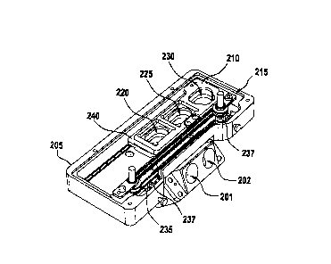
Figure 2 shows a schematic illustration of a filter device
130 for an optical module for a lab-on-a-chip analysis
device according to one exemplary embodiment. The filter
device 130 shown here is similar or corresponds to the
second filter device described on the basis of Figure 1.
Date Recue/Date Received 2021-05-17
CA 03120147 2021-05-17
- 14 -
The optical module includes at least one light path.
According to the exemplary embodiment shown, the filter
device 130 includes a through opening 201 for a light path
and an optional further through opening 202 for a further
light path. For example, the filter device 130 has a length
of less than 250 mm and a width of less than 100 mm.
The filter device 130 includes a carrier element 205, a
filter carrier 210, and a drive unit 215. The carrier
element 205 is arrangeable in the optical module. The filter
carrier 210 is movably arranged on the carrier element 205.
Moreover, the filter carrier 210 includes at least one first
filter region 220 and one second filter region 225, the
filter carrier also includes a third filter region 230 by
way of example here. The drive unit 215 is designed to move
the filter carrier 210 between a first position, in which
the first filter region 220 is arranged in the light path,
and a second position, in which the second filter region
225 is arranged in the light path. When the light path is
guided, for example, through the first through opening 201,
the filter carrier 210 is shown here in the first position.
The drive unit 215 is embodied according to the exemplary
embodiment shown here as a belt drive having a toothed belt
235 and an electric motor. The electric motor can be, for
example, a stepping motor, also called a stepper motor. By
means of the toothed belt 235, it is possible to move the
filter carrier 210 rapidly and position it exactly. Further
tensioning rollers 237 are used for a taut line of the
toothed belt 235.
According to the exemplary embodiment shown here, the
filter carrier 210 is embodied as a linearly movable filter
slide. The filter carrier 210 movable by means of the drive
unit 215 can be moved accordingly along a section of the
Date Recue/Date Received 2021-05-17
CA 03120147 2021-05-17
- 15 -
toothed belt 235, for example, to set the first, the second,
or a further position of the filter carrier.
In addition to the filter carrier 210 as a filter slide,
the filter device 130 according to the exemplary embodiment
shown here includes an optional further filter slide 240.
The further filter slide 240 is movably arranged on the
carrier element 205. The further filter slide 240 also
includes a further first filter region and a further second
filter region. In the position shown here of the filter
carrier 210 as a filter slide and the further filter slide
240, the further first filter region lies under the first
filter region 220 and the further second filter region lies
under the second filter region 225. The drive device 215 is
designed to move the further filter slide 240 between a
further first position, in which the further first filter
region is arranged in the light path, and a further second
position, in which the further second filter region is
arranged in the light path.
Moreover, the filter carrier 210 as a filter slide and the
further filter slide 240 according to the exemplary
embodiment shown here are arranged lying one over another
at least in sections. In addition, the filter slide 210 and
the further filter slide 240 are translationally
displaceable in relation to one another. In this way, it is
possible to displace each one of the filter regions 220,
225, 230 or the further filter regions into the light path.
Moreover, it is possible to combine the filter regions 220,
225, 230 with the further filter regions. In this case,
both the filter regions 220, 225, 230 and also the further
filter regions can be formed according to one exemplary
embodiment as optical filters or as an empty position,
whereby, for example, a chemoluminescence is also
detectable by means of the filter device 130 shown here in
the optical module of a lab-on-a-chip analysis device.
Date Recue/Date Received 2021-05-17
CA 03120147 2021-05-17
- 16 -
According to this exemplary embodiment, the optical module
includes the further light path. In the first position of
the filter slide 210, the first filter region 220 is
arranged in the light path extending through the through
opening 201 and the second filter region 225 is arranged in
the further light path extending through the further
through opening 202. Additionally or alternatively, in the
further first position of the further filter slide 240, the
further first filter region is arranged in the light path
and the further second filter region is arranged in the
further light path.
In an assembled state of the filter device 130 and the
optical module, it is thus possible to carry out a
fluorescence excitation in multiple fluorescent wavelength
ranges in one or more regions or chambers of a lab-on-a-
chip cartridge received in the optical module, and
subsequently to enable a fluorescence detection in multiple
fluorescent wavelength ranges over an image region. Filter
changes of filters arranged in the filter carrier or the
further filter slide 240 are enabled in half of a second on
average by means of the drive unit. For this purpose, the
filter carrier 210 as a filter slide and the further filter
slide 240 are translationally displaced in relation to one
another in order to shift in each case a color filter
received in one of the filter regions 220, 225, 230 or the
further filter regions into an image region in order to
enable detection by means of the image sensor of the optical
module. At least one color filter and one empty position is
contained in each filter slide 210, 240 here. The filter
slides 210, 240 are formed according to one exemplary
embodiment to slide translationally on ball-bearing-mounted
rails. This enables a maintenance-free operation of the
filter slides 210, 240 having more than two and a half
million filter changes. The position of the filter slides
Date Recue/Date Received 2021-05-17
CA 03120147 2021-05-17
- 17 -
210, 240 is detected and monitored by means of a sensor. In
this way, minimized travel distances of the filter slides
210, 240 are enabled during a sequential movement of all
filter elements.
Figure 3 shows a schematic illustration of a filter device
130 for an optical module for a lab-on-a-chip analysis
device according to one exemplary embodiment. A top view of
the exemplary embodiment of the filter device shown in
Figure 2 is shown, accordingly the filter carrier 210 is
arranged as a linearly movable filter slide on the carrier
element 205, and the filter device 130 comprises the further
filter slide 240 and the drive unit 215 as a belt drive.
According to the exemplary embodiment shown here, the
filter slide 210 and the further filter slide 240 are
separately driven by the toothed belt 235 having electric
motor on a drive roller 305, also called a pulley. The
position of the filter slide 210 and of the further filter
slide 240 is monitored according to the exemplary
embodiment shown here by means of a photoelectric sensor
310. For example, the photoelectric sensor 310 is arranged
on a side wall of the carrier element 205, wherein different
positions of the filter slides 210, 240 are associated with
different distances to the photoelectric sensor 310.
Moreover, the first filter region 220 is formed according
to the exemplary embodiment shown here as an optical filter
315 or as an empty position 320. Additionally or
alternatively, the second filter region 225 is formed as an
optical filter 315 or as an empty position 320. By way of
example, the first filter region 220 and the second filter
region 225 are formed as optical filters here, and the third
filter region 230 is formed as an empty position. To form
the empty position 320, for example, a filter opening is
left open, and to form one of the filter regions 220, 225,
230 as an optical filter 315, the optical filter 315 is
Date Recue/Date Received 2021-05-17
CA 03120147 2021-05-17
- 18 -
arranged at the filter opening. When the filter slide 210,
in a state connected to the optical module, is positioned
so that the optical filter 315 arranged in the first filter
region 220, for example a color filter, is arranged in the
image region, thus in the light path, the further filter
slide 240 is thus arranged, for example, so that the empty
position 320 lies below the first filter region 220. Thus,
if one of the filter slides 210, 240 is positioned on the
position of the optical filter 315 as a color filter in the
image region, the other filter slide 210, 240 is thus in
the position of the empty position. If both filter slides
210, 240 are placed on the empty position and the region to
be detected of the lab-on-a-chip cartridge is not
illuminated by the excitation light path, a
chemoluminescence detection, a self-luminous reaction, can
thus be detected. If both filter slides 210, 240 are on the
empty position 320 and another excitation wavelength is
activated in the excitation path, a check image of the
entire image region can thus be recorded.
Figure 4 shows a schematic illustration of a filter device
125 for an optical module for a lab-on-a-chip analysis
device according to one exemplary embodiment. The filter
device 125 shown here is similar or corresponds to the first
filter device described on the basis of Figure 1. According
to the exemplary embodiment shown here, the filter carrier
210 is embodied as a rotatable filter wheel and is also
referred to in the following as a filter wheel 210. Moreover,
the filter device 125 according to the exemplary embodiment
shown here includes an optional further filter wheel 405.
The further filter wheel 405 includes a further first filter
region 410 and a further second filter region 415. By way
of example, the filter wheel 210 and the further filter
wheel 405 each include a third and a fourth filter region
here. The drive unit 215 is designed to move both the filter
wheel 210 and also the further filter wheel 405. The drive
Date Recue/Date Received 2021-05-17
CA 03120147 2021-05-17
- 19 -
unit 215 is thus designed to move the further filter wheel
405 between a further first position, in which the further
first filter region 410 is arranged in the further light
path, and a further second position, in which the further
second filter region 415 is arranged in the further light
path.
According to the exemplary embodiment shown here, the
filter wheels 210, 405 are arranged adjacent to one another
lying in a plane. Moreover, the filter wheel 210 and the
further filter wheel 405 are synchronously rotatable by
means of the toothed belt 235 of the drive unit 215.
The filter wheel 210 and the further filter wheel 405 each
include four filter regions 405, 410 according to the
exemplary embodiment shown here, on which optical filters
are arranged as excitation filters. Moreover, the filter
wheels 210, 405 each also include a black position in order
to block the light of the light source as needed, for
example, a white-emitting excitation light-emitting diode,
for example, to enable a recording of dark images or noise
images, or to carry out a chemoluminescence detection.
The embodiment shown here of the filter device 125
advantageously enables a compact construction having a
width of, for example, less than 200 mm, with the option of
forming five filter regions per filter wheel 210, 405 as
shown here. For example, an arrangement of six filter
positions per filter wheel 210, 405 with two excitation
regions on the lab-on-a-chip cartridge having a diameter of
greater than 2 mm diameter is also possible. An arrangement
of the filter device 125 shown here having the drive unit
215 in the excitation light path of the optical module
advantageously enables a filter change of on average less
than half of a second.
Date Recue/Date Received 2021-05-17
CA 03120147 2021-05-17
- 20 -
Figure 5 shows a schematic illustration of an assembly
having a filter device 125 for an optical module for a lab-
on-a-chip analysis device according to one exemplary
embodiment. The assembly comprises, in addition to the
filter device 125, which is similar or corresponds to the
filter device described on the basis of Figure 4, two light
sources 105 in the form of light-emitting diodes arranged
on the filter device 125. On a side facing toward the filter
device 125, each light source 105 comprises a light guide.
The mechanical components of the assembly shown here for
the optical module are manufactured, for example, from
plastic and aluminum. The components are also black or are
anodized black to minimize reflection and penetration of
light.
The two light sources 105 are implementable, for example,
as white light sources, which are temperature stabilized
and are monitored in intensity by means of a check
photodiode. To excite multiple regions or chambers of the
lab-on-a-chip cartridge, multiple light sources 105 and
filter wheels 210, 405 are accordingly arranged adjacent to
one another, two each here by way of example. For the rapid
filter change, the filter wheels 210, 405 are moved by means
of the drive unit 215 in the form of the belt drive. The
light of the white light-emitting diodes of the light
sources 105 is optionally guided by means of light guides
to the filters and the excitation region on the lab-on-a-
chip cartridge.
According to the exemplary embodiment shown here, the
filter device 125 moreover comprises a sensor 510. The
sensor 510 is embodied here by way of example as a
photoelectric sensor. Moreover, the sensor 510 is designed
to provide a sensor signal representing a positioning of
the filter carrier. The sensor signal can be used to control
the drive unit 215. Moreover, the filter device 125
Date Recue/Date Received 2021-05-17
CA 03120147 2021-05-17
- 21 -
comprises the filter carrier 210 embodied as a filter wheel
and the further filter wheel 405, which are rotatably
arranged on the carrier element 205.
Figure 6 shows a schematic illustration of a filter device
125 for an optical module for a lab-on-a-chip analysis
device according to one exemplary embodiment. The filter
device 125 shown here is similar or corresponds to the
filter devices described on the basis of Figures 4 and 5.
The filter carrier 210 as a filter wheel and the further
filter wheel 405 each include five filter regions here by
way of example, of which one is implemented in each case as
a so-called black position for blocking light and four are
implemented as optical filters. The optical filters are
embodied here, for example, as excitation color filters and
are centrally positioned on the filter wheels 210, 405 and
permanently adhesively bonded in the filter wheels 210, 405.
In this case, the filter regions and thus the color filters
in the filter carrier 210 as a filter wheel and the further
filter wheel 405 are positioned so that in both fields the
same color filter is positioned in each case and two
positions can be excited simultaneously on the lab-on-a-
chip cartridge. The color filters include, for example, the
colors black, gray, red, orange, and blue.
Figure 7 shows a schematic illustration of a part of an
optical module for a lab-on-a-chip analysis device
according to one exemplary embodiment. For example, two
light sources 105 are shown as part of the optical module.
A light guide 705, which has a conical shape, is arranged
on each of the light sources 105. Moreover, two lenses 710
are shown, each of which is arranged on an end of each light
guide 705 facing away from the light source 105. The part
of the optical module shown here also comprises a portion
of the filter carrier 210 as a filter wheel and the further
filter wheel 405. The portions of the filter carrier 210 as
Date Recue/Date Received 2021-05-17
CA 03120147 2021-05-17
- 22 -
a filter wheel and the further filter wheel 405 are each
arranged at an end of one of the lenses 710 facing away
from the light guide 705.
According to the exemplary embodiment shown here, the
optical module comprises more than one light source 105.
Two light-emitting diodes are arranged in parallel as light
sources 105 here by way of example, each having one of the
funnel-shaped light guides 705 and one of the lenses 710.
The filter wheels 210, 405 are placed so that they
communicate with one another by means of gearwheels. A motor
gearwheel moves both filter wheels 210, 405 simultaneously,
as shown on the basis of following Figure 8. These subunits
are unified downstream of the filter wheels 210, 405 and
share the same relay lens. However, the beam paths are
positionally resolved by the lens 710 in the funnel of the
light guide 705. The subunits are symmetrical to one another,
but can also be implemented asymmetrically. The arrangement
of the light sources 105 results from the structure and the
toothing of the filter wheels 210, 405.
Figure 8 shows a schematic illustration of a part of a
filter device 125 for an optical module for a lab-on-a-chip
analysis device according to one exemplary embodiment. The
arrangement is shown of the filter carrier 210 as a filter
wheel and the further filter wheel 405 from the part of the
filter device 125 described on the basis of Figure 7 for
the optical module. The drive unit 215 comprises a motor
gearwheel 805 according to the exemplary embodiment shown
here. The motor gearwheel 805 is designed to rotate the
filter carrier 210 as a filter wheel and the further filter
wheel 405 synchronously in order to set the position of the
filter regions on the filter carrier 210 and the further
filter wheel 405. Teeth of the motor gearwheel 805 engage
directly in gear rims of the filter wheels 210, 405. A
toothed belt can be omitted in this way.
Date Recue/Date Received 2021-05-17
CA 03120147 2021-05-17
- 23 -
Figure 9 shows a schematic illustration of a part of an
optical module for a lab-on-a-chip analysis device
according to one exemplary embodiment. A total field of
view 905 of a camera or the image sensor of the optical
module in combination with the macro lens is shown as part
of the optical module. By means of an exposure unit, which
comprises the light sources which are similar or correspond
to the light sources described on the basis of preceding
figures, two homogeneous spots 910, 911 are generated. The
spots 910, 911 correspond to regions in the lab-on-a-chip
cartridge received in the optical module, which are
illuminated by means of the light sources 105. The spots
910, 911 have a homogeneous illumination in the spot regions
indicated. If a fluorescent mode is used, fluorophores
corresponding to the filter are visible there. If one
selects an analysis filter, more of the surroundings can be
seen due to scattered light and also the entire total field
of view 905 can be observed. Moreover, the spots 910, 911
show regions in which quantitative fluorescent measurements
are possible. Quantitative absorption measurements are also
possible in the region. For incident light images, where
location resolution is required, this can be achieved by
long exposure times and scattered light. The desired
recording region, the field of view to be measured (region
of interest [ROI]), can be selected via software. The
desired recording region theoretically moves between one
pixel and the total field of view 905. The dynamic field of
view selection can be used to reduce the amount of data so
that the entire field of view 905 does not have to be stored
and sent as a data packet. An image can also be constructed
via software by a combination of various desired recording
regions (ROI) from various recordings.
Figure 10 shows a schematic illustration of a lab-on-a-chip
analysis device 1000 having an optical module 100 according
Date Recue/Date Received 2021-05-17
CA 03120147 2021-05-17
- 24 -
to one exemplary embodiment. A lab-on-a-chip cartridge 115
in the form of a disposable microfluidic unit is arranged
in the lab-on-a-chip analysis device 1000. Chemicals and
fluidic channels are located on the lab-on-a-chip cartridge
115. Check, conditioning, functional, and detection units
are integrated into the lab-on-a-chip analysis device 1000
in the form of permanently defined interfaces, for example,
between the optical module 100 and the lab-on-a-chip
cartridge 115. A central checking unit 1005 orchestrates
all of the other units of the lab-on-a-chip analysis device
1000. For this purpose, the checking unit 1005 is connected
so it is capable of signal transmission to the following
units of the lab-on-a-chip analysis device 1000: the
optical module 100, which is also formed as a central
detection unit, an acoustic unit 1010, which can generate
or measure soundwaves, a temperature unit 1015, a user
interface 1020, a pneumatic unit 1025, and a library 1030
having various pieces of software, for example, an assay-
specific evaluation algorithm and a data memory. The
checking unit 1005 executes an assay-specific protocol of
predefined steps. In this case, the checking unit 1005
activates the corresponding units in a chronologically
controlled sequence. The checking unit primarily emits
commands. However, it is also possible that the checking
unit 1005 receives and evaluates data as a response and
then decides about a continuation in the assay protocol and
adapts the protocol dynamically.
In addition to a system like the exemplary embodiment shown
here of the lab-on-a-chip analysis device 100 having the
capacity for processing a microfluidic unit such as the
lab-on-a-chip cartridge 115 shown here, it is possible to
provide a scaled system having the same architecture and
the capacity of processing multiple microfluidic units. In
this case, each microfluidic unit can receive its own,
structurally-identical optical unit in the form of the
Date Recue/Date Received 2021-05-17
CA 03120147 2021-05-17
- 25 -
optical module 100. Alternatively, the microfluidic units
can be arranged so that the optical module 100 is pushed
back and forth by means of a motorized xy stage, thus a
framework movable in two directions, and images are
recorded serially.
Figure 11 shows a flow chart of a method 1100 for operating
an optical module for a lab-on-a-chip analysis device
according to one exemplary embodiment. The method 1100
shown here is usable to operate an above-described
exemplary embodiment of the optical module. The method 1110
comprises a step 1105 of providing a first setting signal,
a step 1110 of providing a second setting signal, a step
1115 of providing a first filter change signal, and a step
1120 of providing a second filter change signal. The first
setting signal in step 1105 is designed to set the filter
carrier of the first filter device in a position associated
with an analysis mode. The position associated with the
analysis mode can be, for example, the first position or
the second position of the filter carrier, as described
above on the basis of Figures 2 and 3. The second setting
signal in step 1110 is designed to set the filter carrier
of the second filter device in a position associated with
the analysis mode. The first filter change signal in step
1115 is designed to set the filter carrier of the first
filter device in a position associated with a further
analysis mode. The second filter change signal in step 1120
is designed to set the filter carrier of the second filter
device in a position associated with the further analysis
mode.
In the following, an exemplary embodiment of the method
1100 and thus an exemplary setting and filter change option
of the first and second filter device of the optical module
is explained by way of example on the basis of various modes
for image recordings: In an analysis mode "blocked", the
Date Recue/Date Received 2021-05-17
CA 03120147 2021-05-17
- 26 -
light path is covered from the direction of the light unit
and in the direction of the detection unit, correspondingly
the filter carriers of the first filter device, also called
a filter LED, and the second filter device, also called a
filter camera, are in a "shutter position". The analysis
mode "blocked" is used, for example, to measure a noise of
a CMOS chip (salt-and-pepper noise). In an analysis mode
"incident light", no filter or an analysis filter is placed
in front of the LED and camera. Various LED filters can
also be received in succession in front of the LED and
summed accordingly. In the analysis mode "incident light"
an analysis or excitation filter is accordingly arranged in
the illuminated filter region of the filter carrier of the
first filter device, and an analysis filter or no filter
insert is arranged in the illuminated filter region of the
filter carrier of the second filter device. The
corresponding excitation and emission filters are used for
fluorescence. In an analysis mode "fluorescence", an
excitation filter is arranged in the corresponding filter
region of the first filter device and an emission filter is
arranged in the filter region of the second filter device.
For a chemoluminescence measurement, the light source is
blocked and the analysis filter is used. In an analysis
mode "chemoluminescence", a "shutter" is located in the
corresponding filter region of the first filter device and
an analysis filter or no filter insert is located in the
filter region of the second filter device. These modes can
be combined with dynamic fields of view (ROI).
Figure 12 shows a schematic illustration of a use of an
optical module for a lab-on-a-chip analysis device
according to one exemplary embodiment. Combinations of
various recording modes with various fields of view are
shown in a sequence of the method. The first recording mode
1205 shows a total field of view by way of example. In this
case, for example, a location of the microfluidic unit,
Date Recue/Date Received 2021-05-17
CA 03120147 2021-05-17
- 27 -
thus the lab-on-a-chip cartridge, can be checked. A
relative coordinate system for the lab-on-a-chip cartridge
can be placed using this information. This is of interest
since any lab-on-a-chip cartridge can be located slightly
displaced in the analysis unit, the lab-on-a-chip analysis
device, due to manufacturing and mechanical conditions.
This information has to be measured once and ROI for
following recordings using the same lab-on-a-chip cartridge
can be dynamically adapted. One can also establish using
such an image whether fluids are present in microfluidic
channels. A second recording mode 1210 shows how an assay
result can be read out by fluorescence. In a next step,
when the first measurement method of the first part is
completed and the sample is further processed, it can be
checked by image recording in the transmitted light mode,
as shown on the basis of a third recording mode 1215,
whether the transition from the first method into the second
has taken place successfully or whether, for example, air
has entered the system or thorough mixing has not taken
place. In the next step, the second method can be recorded
using another recording mode, a fourth recording mode 1220
shown here. In all steps, various filter positions and
fields of view can be recorded using the same optical unit,
the optical module. As an example, an assay is executed
here in which, in a first step, sample material is purified,
an amplification takes place by means of PCR, and the
specificity of the PCR products is detected by means of a
DNA micro-array. In addition to the universal location
image, it can also be measured again and again in the bright
field whether bubbles are in the analyte. A PCR can then be
tracked by means of fluorescence. For example, in real time
or also using a starting point and endpoint measurement.
The micro-array can then be read out by means of
chemoluminescence. Microarrays, which are often spatially
separated from PCR reaction vessels, can thus be arranged
easily according to the described arrangement of the
Date Recue/Date Received 2021-05-17
CA 03120147 2021-05-17
- 28 -
analysis unit system on a lab-on-a-chip cartridge and
connected by means of channels.
Figure 13 shows a schematic illustration of a use of a lab-
on-a-chip analysis device having an optical module
according to one exemplary embodiment. For example, a lab-
on-a-chip analysis device is used as described on the basis
of Figure 10. As an example, a use of the lab-on-a-chip
analysis device for a dynamic progress check of an LoC assay
is shown here. For this purpose, recording is carried out
in a recording mode 1305 shown here. Subsequently, an
evaluation is carried out as marked here by a first block
1310. If a quantitative measurement, for example a
fluorescence measurement, is performed, the result is then
evaluated in situ. If the signal corresponds to typical
values of the assay, the experimental sequence or the
measurement is thus continued, correspondingly the
recording mode 1305 is also still executed. If an anomaly
is established in the measured value, the measurement field
is thus measured in another analysis mode 1315, for example
incident light instead of fluorescence, to analyze what has
resulted in the anomaly. A deviation measurement and a
comparison to known anomalies take place, marked here by a
second block 1320. The deviation measurement is compared
here to a library of possible errors. In each assay, there
are various reasons for occurrence for an anomaly. These
can be checked and analyzed using various recording modes.
The error analysis can then be compared to the library and
a corresponding error message can be returned, marked here
by a third block 1325 "error code". If the error is not
noted in the library, it can also be sent back via
communication interfaces to a platform provider, analyzed,
and received as a new element in the library. The method is
subsequently continued according to instructions from the
library corresponding to the error message, which is marked
here by a fourth block 1330.
Date Recue/Date Received 2021-05-17
CA 03120147 2021-05-17
- 29 -
If an exemplary embodiment comprises an "and/or" linkage
between a first feature and a second feature, this is thus
to be read to mean that the exemplary embodiment includes
both the first feature and also the second feature according
to one embodiment and includes either only the first feature
or only the second feature according to a further embodiment.
Date Regue/Date Received 2021-05-17