Note: Descriptions are shown in the official language in which they were submitted.
CA 03120321 2021-05-17
WO 2020/112871 PCT/US2019/063403
CONTACTLESS ELECTRODE FOR SENSING
PHYSIOLOGICAL ELECTRICAL ACTIVITY
Cross-Reference to Related Applications
[0001] This application claims priority from US Application No. 62/772,242
filed
28 November 2018. For purposes of the United States, this application claims
the benefit
under 35 U.S.C. 119 of US Application No. 62/772,242 filed 28 November 2018
and
entitled CONTACTLESS ELECTRODE FOR SENSING PHYSIOLOGICAL ELECTRICAL
ACTIVITY which is hereby incorporated herein by reference for all purposes.
Technical Field
[0002] The technology described herein relates to electrodes for
electrocardiography
(ECG) systems, electroencephalography (EEG) systems, electromyography (EMG)
systems, electrooculography (EOG) systems and/or similar systems, which detect
physiological electrical activity at locations on, within, or proximate to, an
individual's body.
Background
[0003] A conventional ECG system, for example, typically includes between 3
and 10
electrodes placed on areas of an individual's body to detect electrical
activity of the
individual's heart. The electrodes are connected to an ECG monitor by a
commensurate
number of wires/cables. A conventional ECG electrode typically includes a
resistive sensor
element. A conventional ECG is typically placed directly against the
individual's skin, with
possibly some conductive gel. A number of electrodes are placed against the
individual's
skin to detect the electrical characteristics of the heart (e.g. the current
through or voltage
across the resistive sensor element) at desired vantage points on the
individual's body. The
detected signals are relayed through the wires to the ECG monitor, which is
typically
located on a lab table or the like, away from the individual's body. A signal
processing unit
within the ECG monitor processes the signals to generate an ECG waveform which
can be
displayed on a display of the ECG monitor.
[0004] Figures 1 and 2 show three electrodes 10, 12, 14 arranged in the so-
called
Einthoven's triangle on an individual's body 16. As is known in the art,
electrodes 10, 12
and 14 may be respectively referred to as the Right Arm (RA), Left Arm (LA)
and Left Leg
1
CA 03120321 2021-05-17
WO 2020/112871 PCT/US2019/063403
(LL) electrodes because of the locations that they are commonly placed on body
16. To
generate an ECG signal, various potential differences are determined between
the signals
from electrodes 10, 12, 14. These potential differences are referred to as
"leads". Leads
have polarity and associated directionality. The common leads associated with
the
Einthoven's triangle shown in Figures 1 and 2 include: lead I (where the
signal from RA
electrode 10 is subtracted from the signal from LA electrode 12); lead II
(where the signal
from RA electrode 10 is subtracted from the signal from LL electrode 14); and
lead III
(where the signal from LA electrode 12 is subtracted from the signal from LL
electrode 14).
[0005] In addition to the leads shown in Figure 2, other common leads
associated with
the Einthoven's triangle configuration include: the AVR lead (where one half
of the sum of
the signals from LA and LL electrodes 12, 14 is subtracted from the signal for
RA electrode
10); the ACL lead (where one half of the sum of the signals from RA and LL
electrodes 10,
14 is subtracted from the signal for LA electrode 12); and the AVF lead (where
one half of
the sum of the signals from RA and LA electrodes 10, 12 is subtracted from the
signal for LL
electrode 14). As is known in the art, the AVR lead is oriented generally
orthogonally to lead
III, the AVL lead is oriented generally orthogonally to lead II and the AVG
lead is oriented
generally orthogonally to lead I. The signals from each of these leads can be
used to
produce an ECG waveform 18 as shown in Figure 3. Additional sensors can be
added to
provide different leads which may be used to obtain different views of the
heart activity. For
example, as is well known in the art, sensors for precordial leads V1, V2, V3,
V4, V5, V6
may be added and such precordial leads may be determined to obtain the so-
called 12 lead
ECG.
[0006] Detected physiological electrical activity (e.g. electrical activity
detected using,
an ECG system, EEG system, FOG system, EMG system and/or the like) may, for
example, be used to determine non-electrical physiological parameters, such
as, for
example a respiratory rate of a subject.
[0007] Some issues with traditional ECG technology make it an impediment
for use,
particularly in emergency response situations. The multiple electrodes and
their
corresponding wires may require extensive time to set up which may be critical
in
emergency circumstances. Having to maneuver around and detangle a large number
of
2
CA 03120321 2021-05-17
WO 2020/112871 PCT/US2019/063403
wires can be a nuisance. Multiple electrodes and wires can make it difficult
to move an
individual or administer medical aid to an individual. Further, it is almost
impossible to
connect electrodes and maneuver their corresponding wires in space-limited
settings such
as, for example, within the interior cabins of air planes, buses, cars,
trucks, boats or the like.
Signal noise from movement of the wires and wire tension can also degrade the
quality of
the ECG reading. Multiple wires can be particularly problematic during cardiac
monitoring,
where the ECG wires are attached to an individual for a long time. These
issues with
traditional ECG technology are exacerbated where there is a significant
distance between
the individual and the ECG monitor (i.e. where the electrode wires are long).
EEG systems
(which measure electrical activity of the brain), EMG systems (which measure
electrical
activity of skeletal and/or other muscles) and/or FOG systems (which measure
electrical
activity within the eye) may face similar problems.
[0008] In addition to the problems with wires, current ECG systems use
contact
electrodes. Such contact electrodes typically must be placed in direct contact
with the
individual's skin using an adhesive (e.g. conductive gels). The use of contact
electrodes can
be problematic in some circumstances. By way of non-limiting example, it may
be
undesirable or difficult to remove the individual's clothing in certain
situations ¨ e.g. where
the individual may have privacy concerns, where the individual may have a
condition which
makes it undesirable or difficult to apply current-sensing electrodes to the
skin ¨ e.g. the
individual is suffering from burns to the individual's skin, the individual
has body hair which
must be removed prior to using the contact electrodes, the individual is
allergic and/or has a
sensitivity to the adhesive, the individual is a prematurely born infant
having sensitive and/or
fragile skin or the like. The use of contact electrodes may also expose an
individual to an
electric shock hazard ¨ e.g. failure of isolation circuitry isolating the
contact electrodes from
an electrical power system may result in electric shock of the individual.
Also, EEG systems
often require applying conductive gels between the sensor and the skin of the
individual
and/or abrasion of the individual's skin to create electrical contact between
the sensor and
the skin. It can take a long time (e.g. up to an hour or more) to apply the
gel into EEG caps
and/or nets that are used in EEG sensing systems. The gel used in EEG systems
can
diffuse through hair to create shorts between sensors and can dry out over
time. Whether
gel-coated or not, the caps or nets which hold EEG sensors in contact with
skin can be
3
CA 03120321 2021-05-17
WO 2020/112871 PCT/US2019/063403
uncomfortable for the individual being tested, making long term monitoring
(e.g. a desire
when evaluating certain conditions such as epilepsy) difficult.
[0009] There is a general desire for improved electrode systems for ECG,
EEG, EMG
and/or FOG systems. By way of non-limiting example, there is a general desire
for an
electrode that can provide greater flexibility for use by medical
professionals and/or lay
(non-medical) people in a variety of different circumstances. There is also a
general desire
for an electrode that may be more convenient and/or simple to use than
existing contact
electrodes. There is also a general desire for an improved electrode for
detecting electrical
activity in different locations on and/or within an individual's body, such as
the heart (e.g.
heart muscle), brain, the eyes, skeletal or other muscles, or the like.
[0010] The foregoing examples of the related art and limitations related
thereto are
intended to be illustrative and not exclusive. Other limitations of the
related art will become
apparent to those of skill in the art upon a reading of the specification and
a study of the
drawings.
Summary
[0011] The following embodiments and aspects thereof are described and
illustrated in
conjunction with systems, tools and methods which are meant to be exemplary
and
illustrative, not limiting in scope. In various embodiments, one or more of
the above-
described problems have been reduced or eliminated, while other embodiments
are
directed to other improvements.
[0012] One aspect of the invention provides a system for sensing
biopotentials (i.e.
physiological electrical activity) in an individual. The sensing system may be
contactless.
Such system comprises an electrode for generating a sensing signal indicative
of a
biopotential at a location of a body of the individual and a high input
impedance amplifier
circuit. The electrode comprises an electrically conductive sensing layer
having a sensing
surface, an opposing surface which opposes the sensing surface and one or more
edge
surfaces extending between the sensing surface and the opposing surface. The
sensing
surface is exposed for capacitive coupling to an outer tissue surface of the
individual and is
sensitive to electric field in a location and/or vicinity of the sensing
surface. The electrode
further comprises an electrically conductive guard layer proximate to the
opposing surface
4
CA 03120321 2021-05-17
WO 2020/112871 PCT/US2019/063403
of the sensing layer. The opposing surface of the sensing layer and the guard
layer are
separated by an electrically non-conductive layer. The guard layer
electrically insulates the
sensing layer from electromagnetic interference from electromagnetic energy
that impinges
on the guard layer. The guard layer may also prevent leakage current from
flowing into the
sensing layer (and thereby deteriorating the signal from the sensing layer
and/or the high
input impedance of the amplifier). The sensing layer is electrically coupled
to an input of the
high input impedance amplifier circuit to generate an amplifier output signal
that depends at
least in part on capacitive coupling between the sensing layer and the tissue
surface of the
individual.
[0013] In some embodiments, the electrode comprises an electrically
conductive guard
ring peripherally enclosing the sensing layer. An electrically non-conductive
ring extending
from an edge surface of the sensing layer to an inner edge surface of the
guard ring
separates the sensing layer from the guard ring. The guard ring electrically
insulates the
sensing layer from peripheral electromagnetic interference from peripheral
electromagnetic
energy that impinges on the guard ring. The guard layer may also prevent
leakage current
from flowing into the sensing layer (and thereby deteriorating the signal from
the sensing
layer and/or the high input impedance of the amplifier). In some embodiments,
the high
input impedance amplifier comprises a buffer amplifier for generating a
buffered signal. In
some embodiments, the buffered signal is electrically coupled to one or more
of the guard
layer and the guard ring. In some embodiments, the buffered signal is
identical in amplitude
and phase to the sensing signal. In some embodiments, the electrode comprises
an
electrically conductive grounding layer proximate to the guard layer and
electrically coupled
to a ground signal of the amplifier circuit for insulating one or more of the
guard layer, the
guard ring and the sensing layer from electromagnetic interference from
electromagnetic
energy that impinges on the grounding layer. An electrically non-conductive
layer separates
the grounding layer from the guard layer.
[0014] Another aspect of the invention provides a contactless method for
sensing
biopotentials in an individual, the method comprising the steps of using an
electrode to
generate a sensing signal indicative of a biopotential at a body location of
the individual;
and conditioning the generated sensing signal with a high input impedance
amplifier circuit.
The electrode used to generate the sensing signal comprises an electrically
conductive
CA 03120321 2021-05-17
WO 2020/112871 PCT/US2019/063403
sensing layer having a sensing surface, an opposing surface which opposes the
sensing
surface and one or more edge surfaces extending between the sensing surface
and the
opposing surface. The sensing surface is exposed for capacitive coupling to an
outer tissue
surface of the individual and is sensitive to electric field in a location
and/or vicinity of the
sensing surface. The electrode further comprises an electrically conductive
guard layer
proximate to the opposing surface of the sensing layer and is separated from
the opposing
surface by an electrically non-conductive layer. The guard layer electrically
insulates the
sensing layer from electromagnetic interference from electromagnetic energy
that impinges
on the guard layer.
[0015] Another aspect of the invention provides a contactless system for
sensing
biopotentials in an individual, the system comprising an electrode for
generating a sensing
signal indicative of a biopotential at a location of a body of the individual.
The electrode
comprises an electrically conductive sensing layer having a sensing surface,
an opposing
surface which opposes the sensing surface and one or more edge surfaces
extending
between the sensing surface and the opposing surface. The sensing surface is
exposed for
capacitive coupling to an outer tissue surface of the individual and is
sensitive to electric
field in a location and/or vicinity of the sensing surface. The system further
comprises a high
input impedance amplifier circuit. The sensing layer is electrically coupled
to an input of the
amplifier circuit to generate an amplifier output signal that depends at least
in part on
capacitive coupling between the sensing layer and the tissue surface of the
individual. The
system further comprises a biasing integrator circuit for maintaining at least
a direct current
component of the amplifier output signal within operational voltage limits of
the amplifier
circuit. The biasing circuit generates a biasing signal minimizing drift of
the direct current
component from a reference voltage. The biasing signal is electrically coupled
to a biasing
input of the amplifier circuit.
[0016] Another aspect of the invention provides a contactless method for
sensing
biopotentials in an individual, the method comprising the steps of
capacitively coupling an
electrode to an outer tissue surface of the individual to generate a sensing
signal indicative
of a biopotential at a location of the coupled outer tissue surface;
conditioning the generated
sensing signal with a high input impedance amplifier circuit; and using a
biasing integrator
circuit, maintaining at least a direct current component of the conditioned
signal within
6
CA 03120321 2021-05-17
WO 2020/112871 PCT/US2019/063403
operational voltage limits of the amplifier circuit. The biasing circuit
generates a biasing
signal minimizing drift of the direct current component from a reference
voltage. The
electrode comprises an electrically conductive sensing layer having a sensing
surface, an
opposing surface which opposes the sensing surface and one or more edge
surfaces
extending between the sensing surface and the opposing surface. The sensing
surface is
exposed for capacitive coupling to an outer tissue surface of the individual
and is sensitive
to electric field in a location and/or vicinity of the sensing surface. The
biasing signal is
electrically coupled to a biasing input of the amplifier circuit.
[0017] Another aspect of the invention provides a high input impedance
amplifier circuit
for receiving and conditioning a sensing signal generated by capacitively
coupling the
sensing surface of an electrode to an outer tissue surface of the individual.
The amplifier
circuit comprises a high impedance amplifier for receiving a generated sensing
signal. A
generated guard signal minimizes leakage currents from the sensing surface
maintaining
the amplifier circuit's high input impedance. In some embodiments, the
amplifier circuit
further comprises an integrator circuit for reducing and/or minimizing voltage
drifts that may
result in saturation of the high impedance amplifier.
[0018] In addition to the exemplary aspects and embodiments described
above, further
aspects and embodiments will become apparent by reference to the drawings and
by study
of the following detailed descriptions.
Brief Description of the Drawings
[0019] Exemplary embodiments are illustrated in referenced figures of the
drawings. It
is intended that the embodiments and figures disclosed herein are to be
considered
illustrative rather than restrictive.
[0020] Figure 1 is a schematic illustration of the electrodes of a
conventional ECG
system arranged on the individual's body in an Einthoven's triangle
configuration.
[0021] Figure 2 is a schematic illustration of the electrodes of a
conventional ECG
system arranged in an Einthoven's triangle configuration and a number of
corresponding
leads.
7
CA 03120321 2021-05-17
WO 2020/112871 PCT/US2019/063403
[0022] Figure 3 is a typical ECG waveform of the type that might be
displayed on an
ECG system.
[0023] Figure 4 is a perspective view of an example contactless electrode
system
according to an exemplary embodiment.
[0024] Figure 4A is a plan view of the electrode of the Figure 4 electrode
system.
[0025] Figures 5 is a cross-sectional view of an example embodiment of a
sensing
portion of the Figure 4 electrode.
[0026] Figures 5A-5B are cross-sectional views of example alternative
embodiments of
a sensing portion of the Figure 4 electrode.
[0027] Figure 6A is a block diagram of an example wired embodiment a
contactless
electrode system.
[0028] Figure 6B is a block diagram of an example wireless embodiment of a
contactless electrode system.
[0029] Figure 60 is a block diagram of an example multi-sensor embodiment
of a
contactless electrode system.
[0030] Figure 7 is an electrical schematic illustration of an amplifier
circuit suitable for
use with the Figure 4 electrode system according to an exemplary embodiment.
[0031] Figures 7A-D are electrical schematic illustrations various example
embodiments
of an amplifier circuit suitable for use with the Figure 4 electrode system.
[0032] Figure 8A is a graph depicting simulation results which show
undesirable
saturation in an amplifier circuit. Figure 8B is a graph depicting simulation
results of an
amplifier circuit comprising an integrator circuit to mitigate the saturation
issue in Figure 8A.
[0033] Figure 9 is a schematic illustration of making biopotential
measurements using a
current sense amplifier and two contactless electrodes.
8
CA 03120321 2021-05-17
WO 2020/112871 PCT/US2019/063403
[0034] Figure 10 is a schematic illustration of an example ECG system
incorporating
the Figure 4 electrode system.
[0035] Figure 11 is a perspective view of an example portable device
incorporating the
Figure 4 electrode system.
Description
[0036] Throughout the following description specific details are set forth
in order to
provide a more thorough understanding to persons skilled in the art. However,
well known
elements may not have been shown or described in detail to avoid unnecessarily
obscuring
the disclosure. Accordingly, the description and drawings are to be regarded
in an
illustrative, rather than a restrictive, sense.
[0037] Figure 4 illustrates a perspective view of an electrode system 100
according to
an example embodiment. Electrode system 100 of the Figure 4 embodiment
comprises a
contactless electrode 120 (e.g. an electrode capable of sensing biopotentials
of a subject
without contacting the body of the subject) removably coupled to a housing 141
enclosing
an amplifier circuit 140. In some embodiments, amplifier circuit 140 has high
input
impedance to avoid loading contactless electrode 120. In some embodiments, it
is not
necessary that electrode system 100 be contactless and a contact-based
electrode (not
shown) may be provided in addition to, or in the alternative to, contactless
electrode 120.
Contactless electrode 120 is electrically connected to amplifier circuit 140
through suitable
electrical wirings, leads, pins, pads or the like.
[0038] Housing 141 may, for example, be fabricated from electrically
conductive
material and may electrically shield (i.e. isolate) amplifier circuit 140 from
external undesired
electromagnetic interference from electromagnetic energy that impinges on
housing 141. In
some embodiments, housing 141 may be hermetically sealed. Hermetic sealing of
housing
141 prevents moisture, dust, debris or the like from entering housing 141 and
possibly
having a deleterious impact on the input impedance or other performance
characteristics of
amplifier circuit 140. Housing 141 may, for example, be sealed using an epoxy
resin or the
like.
9
CA 03120321 2021-05-17
WO 2020/112871 PCT/US2019/063403
[0039] In the Figure 4 example embodiment, contactless electrode 120
comprises a
sensing portion 122 and a projection member 138. Projection member 138 may
extend
outwardly from sensing portion 122 of electrode 120. The length of projection
member 138
may be longer than that of sensing portion 122. Projection member 138 may be
flexible.
Projection member 138 may include electrically conductive contact plates 139
(see Fig. 4A)
on a distal end of projection member 138. Sensing portion 122 of electrode 120
may, for
example, be electrically coupled (e.g. routed) to contact plates 139 via
electrical leads
and/or contacts (not explicitly shown), as described herein.
[0040] Projection member 138 may be connected to housing 141 through a
suitably
configured electrical connection port 142 of housing 141. Connection port 142
may
comprise electrically conductive contact plates 142A engageable with contact
plates 139 of
electrode 120. Projection member 138 may be mechanically coupled to connection
port 142
to electrically engage contact plates 139 and142A to electrically couple
electrode 120 with
amplifier circuit 140. Contact plates 139 and 142A may be fabricated from
gold, silver,
copper, other conductive metals, combinations thereof and/or the like.
[0041] Sensing portion 122 may be brought into proximity of the body (e.g.
skin) of an
individual, where sensing portion 122 may be capacitively coupled to the
individual's outer
tissue surface, so that sensing portion 122 is sensitive to (e.g. exhibits a
capacitance or
otherwise generates an electrical signal that depends on) electric field in a
location and/or
vicinity thereof. Sensing portion 122 may, for example, be capacitively
coupled to anterior
(i.e. front) and/or posterior (i.e. rear) outer tissue surfaces of the
individual. More
specifically, placement of sensing portion 122 in proximity to an outer tissue
surface of the
individual exposes sensing portion 122 to one or more electric fields
corresponding to one
or more measurable biopotentials (e.g. electrical activity within the
individual). Exposure of
sensing portion 122 to such electric field causes sensing portion 122 to
exhibit an electrical
sensing signal 105 (Figure 7) representative, at least in part, of the
electric field to which
sensing portion 122 was exposed. Advantageously, physical contact between
sensing
portion 122 and an outer tissue surface is not required for generation of
sensing signal 105.
In some embodiments, electrode 120 may measure biopotentials within an
individual
without removal of the individual's clothing.
CA 03120321 2021-05-17
WO 2020/112871 PCT/US2019/063403
[0042] In the Figure 4 example embodiment, sensing portion 122 is circular,
although
this is not necessary. A surface area of sensing portion 122 may be varied,
for example,
depending on biopotentials to be measured and/or physical size constraints
(e.g. EEG
requires many electrodes in close vicinity of one another). For example, a
diameter of
50mm (or surface area of -2000mm2) may be suitable for measurement of
biopotentials for
an ECG system. A diameter of 20mm (or a surface area of -315mm2) may, for
example, be
suitable for measurement of biopotentials for an EEG or EMG system. The
sensing surface
of sensing portion 122 may be triangular, elliptical, rectangular,
trapezoidal, hexagonal,
octagonal or any other suitable shape. In some embodiments, electrode 120 is
flexible
allowing electrode 120 and sensing portion 122 to adapt and/or conform to body
contours
which may be individual specific.
[0043] Figure 5 illustrates a vertical cross-sectional view of sensing
portion 122 of the
Figure 4 electrode 120 according to an example embodiment. Sensing portion
122, as
illustrated, is multi-layered comprising a plurality of electrically
conductive layers 124, 126,
128 (shown as hatched in Figure5) and an electrically conductive ring 130
(also shown as
hatched) layered in between electrically non-conductive insulating layers
123A, 123B,
1230, 123D (collectively insulating layers 123 - shown as white in Figure 5)
and an
electrically insulating ring 131 (also shown as white).
[0044] In some embodiments, electrically conducting ring 130 is concentric
with
electrically insulating ring 131. In some embodiments, electrically insulating
ring 131 is
enclosed by electrically conducting ring 130. In some embodiments, an inner
circumference
of electrically conducting ring 130 contacts an outer circumference of
electrically insulating
ring 131. In some embodiments, electrically conducting ring 130 and
electrically insulating
ring 131 are located in a second layer of the plurality of layers of sensing
portion 122.
[0045] In the Figure 5 embodiment conductive layer 124 provides a sensing
layer.
Sensing layer 124, which is proximate to a sensing side 122A of sensing
portion 122, is
sensitive to electric field associated with biopotentials. In some
embodiments, sensing layer
124 is located in the second layer comprising the electrically conducting ring
130 and the
electrically insulating ring 131 described above.
11
CA 03120321 2021-05-17
WO 2020/112871 PCT/US2019/063403
[0046] Sensing layer 124 may be described as an antenna for receiving one
or more
electric fields corresponding to electrical activity within the body of the
individual. One or
more electric fields associated with biopotentials from the individual excites
electrons within
sensing layer 124 generating sensing signal 105 representative of the
biopotentials.
Electrical lead(s) or contact(s) (not explicitly shown) within electrode 120
may, for example,
electrically couple sensing layer 124 to contact plates 139 described herein.
Insulating layer
123A extending across an outer sensing surface 124-1 of sensing layer 124
protects
sensing layer 124 from exposure to external environmental elements such as,
for example,
moisture, dust, bodily fluids or the like. Insulating layer 123A, in
combination with insulating
layer 123D, also facilitates disinfection and/or cleaning of sensing side 122A
and non-
sensing side 122B of sensing portion 122.
[0047] External electromagnetic interference, such as, for example, from
cellular
phones, VVi-Fi routers, Bluetooth coupled devices, cordless telephones,
inductive chargers,
multimedia displays, power lines and/or the like may reduce a signal-to-noise
ratio (SNR) of
sensing signal 105. In particular embodiments, as shown in Figure 5, for
example, sensing
portion 122 comprises one or more of electrically conductive elements which
may include:
guard layer 126, guard ring 130 and/or grounding layer 128. In such
embodiments, guard
layer 126 may extend across an opposing surface 124-2 of sensing layer 124
(i.e. a surface
124-2 opposing sensing surface 124-1). Guard ring 130 may peripherally enclose
edge
surfaces 124-3 of sensing layer 124. Insulating layer 123B and/or insulating
ring 131 may
be located between guard layer 126 and guard ring 130 to electrically isolate
guard layer
126 and guard ring 130 from sensing layer 124. Electrical lead(s) or
contact(s) (not explicitly
shown) within electrode 120 may, for example, electrically couple guard layer
126 and/or
guard ring 130 to contact plates 139 described herein.
[0048] In some embodiments, guard layer 126 and/or guard ring 130 are
electrically
coupled to amplifier circuit 140 to receive buffer signal 159 from amplifier
158, as described
elsewhere herein (see discussion of Figure 7). Buffer signal 159, as described
herein, may
be similar or substantially identical in amplitude and phase to sensing signal
105 generated
from sensing layer 124 (in preferred embodiments buffer signal 105 is
identical to sensing
signal 105). In such embodiments, continuously receiving buffer signal 159 at
guard layer
126 and/or guard ring 130 equalizes electric potentials across sensing layer
124 and guard
12
CA 03120321 2021-05-17
WO 2020/112871 PCT/US2019/063403
layer 126 and/or guard ring 130, thereby preventing extraneous current flow
between
sensing layer 124 and guard layer 126 and/or guard ring 130. In this manner,
sensing layer
124 may be actively electrically shielded from external electromagnetic
interference from
electromagnetic energy which impinges on guard layer 126 and/or guard ring 130
and/or
from leakage currents escaping sensing layer 124. Preventing extraneous
current flow to
and/or from sensing layer 124 desirably maintains a high input impedance of
amplifier
circuit 140. Guard layer 126 and guard ring 130 may, for example, reduce
leakage currents
from sensing layer 124 and/or impingement of external electromagnetic
interference on
sensing layer 124, thereby maintaining the high input impedance of amplifier
circuit 140,
even in embodiments where buffer signal 159 is not entirely identical in
amplitude and
phase to sensing signal 105.
[0049] Grounding layer 128 of the illustrated embodiment is proximate to
non-sensitive
side 122B of sensing portion 122 (alternatively, grounding layer 128 may be
referred to as
"shielding layer 128"). Grounding layer 128 may further improve the SNR of
sensing signal
105 by, for example, further minimizing effects of external electromagnetic
interference on
sensing layer 124, guard layer 126 and/or guard ring 130.
[0050] Grounding layer 128 is electrically coupled to ground signal 172 of
amplifier
circuit 140. Impingement of external electromagnetic interference on grounding
layer 128
electrically grounds any impinging electromagnetic interference precluding
such
electromagnetic interference from impinging sensing layer 124, guard layer 126
and/or
guard ring 130. Insulating layer 1230 extending across an internal surface of
grounding
layer 128 electrically isolates grounding layer 128 from guard layer 126.
Insulating layer
123D extending across an exterior surface of grounding layer 128 protects
grounding layer
128 from exposure to external environmental elements such as, for example,
moisture,
dust, bodily fluids or the like. Electrical lead(s) and/or contact(s) (not
explicitly shown) within
electrode 120 may, for example, electrically couple grounding layer 128 to
contact plates
139 described herein.
[0051] Electrically conductive layers 124, 126, 128 and electrically
conductive ring 130
(i.e. sensing layer 124, guard layer 126, grounding layer 128 and guard ring
130
respectively) may, for example, be fabricated from or otherwise comprises any
suitable
13
CA 03120321 2021-05-17
WO 2020/112871 PCT/US2019/063403
electrically conductive material such as gold, silver, copper, other
conductive metals,
electrically conductive polymer, combinations thereof and/or the like. In some
embodiments,
electrically conductive layers 124, 126, 128 and electrically conductive ring
130 may, for
example, be fabricated from a uniform material. In other embodiments,
electrically
conductive layers 124, 126, 128 and electrically conductive ring 130 may be
fabricated from
different materials. In some embodiments, electrically conductive layers 124,
126, 128
and/or electrically conductive ring 130 are flexible. This may be the case,
for example, when
such layers are fabricated from electrically conductive polymers.
[0052] Electrically insulating layers 123 and electrically insulating ring
131 are
electrically non-conductive. For example, insulating layers 123 and insulating
ring 131 may
comprise one or more dielectric materials, such as polyethylene, polyimide,
polypropylene,
other suitable plastics and/or the like. In some embodiments, electrically
insulating layers
123 and electrically insulating ring 131 may be fabricated from a uniform
material. In other
embodiments, electrically insulating layers 123 and electrically insulating
ring 131 may be
fabricated from different materials. In some embodiments, electrically
insulating layers 123
and electrically insulating ring 131 are flexible.
[0053] In some embodiments, guard ring 130 may be excluded (e.g. removed)
from
sensing portion 122 of electrode 120, as illustrated in Figure 5A. In such
embodiments,
insulating ring 131 peripherally encloses outer edge surfaces 124-3 of sensing
layer 124
and extends outwards from an outer edge surface 124-3 of sensing layer 124 to
an outer
edge surface of sensing portion 122 of electrode 120. Such embodiments, may be
preferable, for example where the dimensions (e.g. the thickness) of outer
edge surface(s)
124-3 is relatively small.
[0054] In some embodiments, guard layer 126 may be excluded (e.g. removed)
from
sensing portion 122 of electrode 120, as illustrated in Figure 5B. Such
embodiments, may
be preferable, for example where it is desirable to minimize the number of
components of
electrode 120 and/or amplifier circuit 140.
[0055] In some embodiments, electrode 120 is flexible (i.e. one or more
components of
electrode 120 are flexible). In some such embodiments, electrode 120 may, for
example,
conform to one or more body contours of the individual. For electrode 120 to
be flexible,
14
CA 03120321 2021-05-17
WO 2020/112871 PCT/US2019/063403
electrically conductive layers 124, 126, 128, electrically conductive ring 130
and/or contact
plates 139 may be mounted onto flexible PCBs. Each flexible PCB may, for
example,
comprise a flexible plastic substrate (e.g. a substrate fabricated from
polyimide, conductive
polyester film or other suitable flexible plastic material), PEEK or the like.
In some
embodiments, multiple conductive components may be mounted on a single
flexible PCB
(e.g. mounting contact plates on a single flexible PCB). In some embodiments,
a flexible
PCB may comprise multiple conductive components mounted on different
electrically
isolated layers of the PCB (e.g. mounting electrically conductive layers 124,
126, 128 on
different electrically isolated layers of a single flexible PCB).
[0056] Figure 6A is a block diagram of an example wired embodiment of
contactless
electrode system 100A. Contactless electrode system 100A comprises a cable
110. Cable
110 electrically couples amplifier circuit 140 to a base unit 180. Base unit
180 may comprise
suitable hardware for receiving and processing amplified signal 160 from
amplifier circuit
140. Examples of suitable hardware include, but are not limited to: analogue
to digital
converters, processors, controllers, displays, etc.
[0057] In a currently preferred embodiment, cable 110 is bidirectional
electrically. Cable
110 may transmit an amplified signal 160 from amplifier circuit 140 to base
unit 180
concurrently with transmitting a signal at the level of power supply 170 and a
ground signal
172 which supply electrical power 170 and a ground reference 172 from base
unit 180 to
amplifier circuit 140.
[0058] Contactless electrode system 100A may be the preferred embodiment
for use in
hospital settings. For example, contactless electrode system 100A may be
especially
suitable for use in the intensive care unit (ICU), intensive therapy unit
(ITU), Neonatal
Intensive Care Unit (NICU) and/or critical care unit (CCU) of a hospital.
[0059] Figure 6B is a block diagram of an example wireless embodiment of
contactless
electrode system 101B. Contactless electrode system 100B digitizes amplified
signal 160
on board before transmitting a corresponding signal to base unit 180.
Contactless electrode
system 100B may transmit data to and/or receive data from base unit 180
wirelessly.
Contactless electrode system 101B comprises suitable analogue to digital
converters 145,
CA 03120321 2021-05-17
WO 2020/112871 PCT/US2019/063403
transmitters 146, and receivers 147 for communicating signals wirelessly
between amplifier
circuit 140 and base unit 180.
[0060] By transmitting amplified signal 160 to base unit 180 wirelessly,
contactless
electrode system 100B may be adapted for use in non-hospital settings, as
described
elsewhere herein. For example, contactless electrode system 100B may be
installed in
cars, beds, cellphone cases, clothing, etc. Contactless electrode system 100B
may transmit
and/or receive signals from a wide range of base units 180B including, but not
limited to:
mobile phones, smart watches, personal computers, engine control modules (in a
car), etc.
[0061] In some embodiments, housing 141 encloses amplifier circuit 140,
digital
converters 145, transmitters 146, and receivers 147. In some embodiments, some
or all of
amplifier circuit 140, digital converters 145, transmitters 146, and receivers
147 are
fabricated on the same circuit board.
[0062] Figure 60 is a block diagram of a contactless electrode system 1000
according
to an example embodiment. Contactless electrode system 1000 comprises a
plurality of
electrodes 120-1, 120-2....., 120-N electrically coupled to a plurality of
corresponding
amplifier circuits 140-1, 140-2, ..., 140-N. A transmission module 111
transmits amplified
signals 160-1, 160-2, ..., 160-N from amplifier circuits 140-1, 140-2, ...,
140-N to base unit
180. In some embodiments, transmission module 111 comprises one or a plurality
of cables
110. In some embodiments, transmission module 111 comprises suitable analogue
to digital
converters 145, transmitters 146, and receivers 147 for transmitting signals
wirelessly to
base unit 180.
[0063] In the example embodiment shown in Figure 60, electrodes 120-1, 120-
2.....
120-N and their corresponding amplifier circuits 140-1, 140-2, ..., 140-N are
contained in
the same housing 141 although this is not necessary. In some embodiments,
electrodes
120-1, 120-2....., 120-N and their corresponding amplifier circuits 140-1, 140-
2, ..., 140-N
are fabricated on the same printed circuit board. In some embodiments,
electrodes 120-1,
120-2....., 120-N and their corresponding amplifier circuits 140-1, 140-2,
..., 140-N are built
as a single pad. The pad may be made of a suitably flexible material (e.g.
silicone) which
facilitates easy sanitization.
16
CA 03120321 2021-05-17
WO 2020/112871 PCT/US2019/063403
[0064] Contactless electrode system 1000 may optionally receive signals
such as
control signals and/or power signals from base unit 180. Contactless electrode
system
1000 may optionally incorporate suitable sensor selection algorithms. The
sensor selection
algorithms may advantageously make contactless electrode system 1000 adaptable
for
patients with different body sizes and may also achieve optimal ECG signals by
selecting
sensors to minimize or mitigate noise, artifacts and/or the like and/or to
maximize signal
amplitude.
[0065] In some embodiments (e.g. see Figs 6A-60), transmitting an amplified
signal
160 to base unit 180 advantageously improves signal to noise ratio.
[0066] In some embodiments, housing 141 comprises suitable silicone
materials which
may advantageously allow for improved sanitization of housing 141. In some
embodiments,
housing 141 comprises suitable fabric materials which may advantageously allow
system
100 to be worn by a patient (e.g. as part of clothing). In some embodiments,
housing 141 is
made of suitable waterproof materials such that housing 141 with its enclosed
components
(e.g. electrodes 120, amplifier circuits 140, etc.) is washable. In some
embodiments,
housing 141 is made of suitable fireproof materials. In some embodiments,
housing 141 is
made of suitable materials that are flexible.
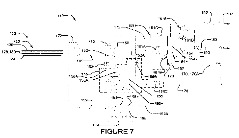
[0067] Figure 7 schematically shows an amplifier circuit 140 suitable for
use with
electrode 122 according to an example embodiment.
[0068] Amplifier circuit 140 comprises a first amplifier 152 for receiving
sensing signal
105 from sensing portion 122 of electrode 120 (e.g. from sensing layer 124).
In the Figure 7
illustrated embodiment, sensing signal 105 is input to amplifier 152 by, for
example,
electrically coupling sensing layer 124 to non-inverting input 152+ of
amplifier 152 using any
method described herein or known in the art. Amplifier 152 is configured as a
unity gain
amplifier (i.e. an amplifier having a voltage gain of 1) by feeding back
output signal 152A to
the inverting input 152- of amplifier 152 in the Figure 7 example embodiment,
although this
is not necessary.
[0069] To maximize the sensitivity of amplifier circuit 140 to sensing
signal 105,
amplifier 152 may, for example, be a high input impedance amplifier. High
input impedance
17
CA 03120321 2021-05-17
WO 2020/112871 PCT/US2019/063403
of amplifier 152 (as a result of amplifier 152 having a low bias current)
reduces electrical
loading of sensing signal 105. Reducing electrical loading of sensing signal
105 can
advantageously allow amplifier circuit 140 to receive a larger sensing signal
105 (compared
to a smaller sensing signal 105 if amplifier 152 did not have a high input
impedance).
[0070] In some embodiments, amplifier 152 may, for example, be a low input
bias
current operational amplifier. In some embodiments, amplifier 152 may comprise
a low input
bias current operational amplifier manufactured by Texas Instruments of
Dallas, Texas
under part number LM P7721 or the like. In some embodiments, amplifier 152 has
a
minimum specified input bias current of 3fA (i.e. 3 femtoamperes). In some
embodiments,
amplifier 152 has a maximum specified input bias current of 90fA (at 85 C).
[0071] Second amplifier 154 of amplifier circuit 140 may amplify output
signal 152A of
first amplifier 152, thereby generating amplified signal 160. Output signal
152A may, for
example, be input into amplifier 154 at non-inverting input 154+ of amplifier
154.
[0072] In some embodiments, as illustrated in Figure 7, output signal 152A
may first
pass through a high-pass filter 157 (e.g. a first degree high-pass filter, as
is the case of the
illustrated embodiment, or some higher order filter). High-pass filter 157 may
comprise, for
example, a capacitor 161A and a resistor 161B, as is the case with the
illustrated
embodiment of Figure 7. Capacitor 161A electrically couples output 152A of
first amplifier
152 to non-inverting input 154+ of second amplifier 154. Resistor 161B
electrically couples
reference voltage 178 to non-inverting input 154+. Varying capacitance of
capacitor 161A
and/or resistance of resistor 161B varies a frequency response of high-pass
filter 157. In
some embodiments, capacitor 161A and resistor 161B may, for example, have a
capacitance of 1pF and a resistance of 887k0 respectively. Increasing the
capacitance of
capacitor 161A and/or the resistance of resistor 161B raises a cut-off
frequency of high-
pass filter 157. Conversely, decreasing the capacitance of capacitor 161A
and/or the
resistance of resistor 161B lowers the cut-off frequency of high-pass filter
157. An ideal
frequency response of high-pass filter 157 may be different for different
biopotentials (e.g.
ECG vs EEG, ECG vs EMC, etc.). High-pass filter 157 may advantageously
eliminate low
frequency noise corresponding to slow motion artifacts, such as the
acceleration or
deceleration of a vehicle in a vehicular application.
18
CA 03120321 2021-05-17
WO 2020/112871 PCT/US2019/063403
[0073] Amplifier 154 may be suitably arranged and electrically connected to
suitable
resistors and/or capacitors to control its gain, corner low frequency, corner
high frequency,
etc. In the example embodiment shown in Figure 7, resistor 161B may bias
amplifier 154 by
setting a steady state output voltage of amplifier 154 to a vicinity of a
specific voltage.
Resistor 161B may also, in combination with resistors 1610, 161D and capacitor
161F, form
a gain stage of amplifier 154. Voltage gain of amplifier 154 may be varied by
varying
resistances of one or more of resistors 1610, 161D. Frequency response of
amplifier 154
may be varied by varying resistance of one or more of resistors 1610, 161D
and/or varying
capacitance of one or more of capacitors 161E, 161F. Resistor 1610 and
capacitor 161F
(electrically coupled in series as shown in Figure 7) may set a corner low
frequency of
amplifier 154. Resistor 161D and capacitor 161E (electrically coupled in
parallel as shown in
Figure 7) may set a corner high frequency of amplifier 154. For example,
decreasing the
resistance of resistor 161D and/or capacitance of capacitor 161E may increase
the corner
high frequency of amplifier 154 (i.e. increases the frequency response
bandwidth of
amplifier 154). In some embodiments, amplifier 154 has a voltage gain in a
range of 2-20. In
some embodiments, this range is 5-15. In some embodiments, this range is 6-12.
Other
levels of gain are possible.
[0074] It may be desirable for amplifier circuit 140 to use different
corner high (i.e. cut-
off) frequencies for different applications (e.g. ECG vs. EEG, EEG vs. EMG,
etc.). In some
embodiments, resistors 1610, 161D may have resistances of 10k0 and 100k0
respectively
and capacitors 161E, 161F may have capacitances of 4,700pF and 22pF
respectively. In
some such embodiments, amplifier 154 has a voltage gain of 11 (1+R4/R3), a
corner low
frequency of 0.72Hz and a corner high frequency of 338.62Hz. In some
embodiments (e.g.
some EEG systems), resistors 1610, 161D may have resistances of 5k0and 50k0
respectively or capacitors 161E, 161F may have capacitances of 2350pF and 11pF
respectively. Other values of resistances, capacitances, gains and corner high
frequencies
may be used.
[0075] In some embodiments, one or more of passive electrical components
161 (e.g.
resistors 161B, 1610, 161D and/or capacitors 161A, 161E, 161F) may, for
example, be
tunable (i.e. resistance and/or capacitance values may be varied) in real-time
and/or in a
calibration context, thereby varying voltage gain and/or frequency response of
amplifier 154
19
CA 03120321 2021-05-17
WO 2020/112871 PCT/US2019/063403
in real-time and/or in a calibration context. Real-time tuning and/or pre-use
calibration of
amplifier 154 may, for example, generate an amplified signal 160 optimized for
a use-
specific purpose (e.g. ECG specific, EEG specific, etc).
[0076] Amplified signal 160 output from amplifier 154 may, for example, be
transmitted
to base unit 180 using cable 110 (Figure 4) as described herein. Optionally,
amplified signal
160 may pass through resistor 163 prior to being received by cable 110.
Optional resistor
163 may electrically safeguard amplifier 154 and/or amplifier circuit 140 from
adverse
electrical events such as, for example, high capacitive loading of cable 110
and/or base unit
180, an electrical short circuit within cable 110 or the like. In some
embodiments, resistor
163 may have a resistance in the range of 100 to 1000.
[0077] Amplifier circuit 140 may further comprise a buffer amplifier 158.
Buffer amplifier
158 may be used to generate a buffer signal 159 receivable by guard layer 126
and/or
guard ring 130 (if guard ring 130 is included) of sensing portion 122 of
electrode 120. As
described herein, buffer signal 159 may be used to reduce adverse impacts of
external
electromagnetic interference and/or leakage currents on sensing plate 124
and/or maintain
the high-input impedance of amplifier circuit 140. In preferred embodiments,
output signal
159 is similar and substantially identical in amplitude and phase to sensing
signal 105. In
such embodiments, output signal 152A of amplifier 152 is input to buffer
amplifier 158 at
non-inverting input 158+ of buffer amplifier 158. Amplifier 158 is configured
as a unity gain
amplifier (i.e. having a voltage gain of 1) by directly feeding buffer signal
159 back to buffer
amplifier 158 at inverting input 158- in the Figure 7 example embodiment,
although this is
not necessary.
[0078] In some embodiments, amplifier circuit 140 comprises optional
resistor 165
which samples inverting input 154- of second amplifier 154 to generate a "COM"
signal 167.
Resistor 165 may, for example, have a resistance in the range of 470 to 1000.
In
biopotential measurement systems comprising multiple electrode systems 100
(such as, for
example, in the embodiment shown in Figure 60 and Figure 10), a plurality of
"COM"
signals 167 may be combined to generate a common mode node. In such
embodiments,
the generated common mode node may be used, for example, for common mode
interference rejection (e.g. rejection of external electromagnetic
interference received by an
CA 03120321 2021-05-17
WO 2020/112871 PCT/US2019/063403
individual's body as a result of the body acting as an antenna or otherwise
common to
multiple electrodes). Common mode interference rejection may be implemented by
capacitively feeding back the common mode node to an individual's body using
one or more
of electrode systems 100. This approach may, for example, be termed "Right Leg
Drive"
(RLD) and/or "Driven Right Leg" (DRL). "COM" signal 167 may, for example, be
transmitted
from amplifier circuit 140 to base unit 180 using cable 110. In some
embodiments, "COM"
signal 167 is wirelessly transmitted from amplifier circuit 140 to base unit
180 using a
suitable wireless communication interface.
[0079] In some embodiments, amplifier circuit 140 comprises a resistor 153
to bias non-
inverting input 152+ of amplifier 152 (i.e. the input impedance of amplifier
circuit 140 is
dependent at least in part on resistor 153). In some embodiments, input
impedance of
amplifier circuit 140 is equivalent to a resistance value of resistor 153
(i.e. in embodiments
where the resistance value of resistor 153 is small (e.g. 10GQ) when compared
to an input
impedance of amplifier 152). In other embodiments, input impedance of
amplifier circuit 140
is equivalent to a total resistance value of resistor 153 in parallel with the
input impedance
of amplifier 152.
[0080] Varying input impedance of amplifier circuit 140 may, for example,
vary
sensitivity of contactless electrode system 100. In such embodiments, a
desired use-
specific (e.g. ECG specific, EEG specific, etc.) sensitivity may be set by
varying resistance
of resistor 153. Sensitivity of amplifier circuit 140 to sensing signal 105
may be increased or
decreased by increasing or decreasing resistance of resistor 153 respectively.
For example,
a resistance value of resistor 153 between 1GO and 10GO may be suitable for
ECG
measurements. For EEG measurements which typically make use of relatively high
sensitivity, resistor 153 may, for example, have a resistance up to 50GQ. In
some
embodiments, resistor 153 may be tuned (e.g. its resistance value may be
varied) in real-
time or during a calibration phase. In some embodiments, as shown in Figure 7,
resistor
153 may have a resistance value of 1GQ.
[0081] In prior art embodiments, a suitable resistor, like resistor 153 is
typically
configured to directly electrically couple a reference voltage (e.g. typically
set at 1/2 of the
power supply voltage 170) to non-inverting input 152+ of first amplifier 152
to thereby
21
CA 03120321 2021-05-17
WO 2020/112871 PCT/US2019/063403
statically bias non-inverting input 152+ at this DC voltage level. However,
this approach
(merely statically setting the DC bias at input 152+), in combination with one
or more other
factors, such as, for example, internal voltage drifting of amplifier 152,
impingement of
electromagnetic interference on sensing layer 124, movement of the subject
and/or
electrode 120 varying capacitance between sensing layer 124 and the subject,
etc., may
result in saturation of high input impedance amplifier 152.
[0082] Saturation of amplifier 152 may, for example, result in an inability
to faithfully
pass sensing signal 105 through amplifier 152 (e.g. see Figure 8A). Passively
biasing
amplifier 152 in this manner, allows input amplitude fluctuations at inputs
152+, 152- of
amplifier 152 to saturate amplifier 152. By way of none limiting examples,
input amplitude
fluctuations may be caused by an individual's (e.g. the individual being
sensed) movement
creating electrostatic charge, movement of other individuals impacting the
electromagnetic
fields, drift of a direct current (DC) operating voltage of amplifier 152 as a
result of operating
temperature drifts, movement of the DC operating voltage as a result of low
frequency
and/or DC electric fields and/or the like. If amplifier 152 is saturated,
output signal 152A of
amplifier 152 is electrically driven to (and clipped at) either zero volts or
the level of the DC
supply voltage 170, thereby impeding sensing signal 105 from being passed
through
amplifier 152. In some embodiments, 20 to 30 seconds may elapse prior to
amplifier 152
settling back to normal (i.e. steady state) operating conditions resulting in
a loss of (i.e.
inability to pass through) sensing signal 105 during that time.
[0083] As an alternative to passively electrically coupling resistor 153 to
power supply
level 170 or reference voltage 178, in particular embodiments of the
invention, amplifier
circuit 140 comprises a biasing integrator circuit 155 (shown in dashed lines
in Figure 7) for
generating an output signal 156A that may be electrically coupled to amplifier
152 (e.g. via
resistor 153 to non-inverting input 152+). As will be explained in more detail
below (see
Figures 8A, 8B), integrator circuit 155 minimizes or reduces voltage drifts at
input 152+
which may cause saturation of amplifier 152. In some embodiments, integrator
circuit 155
comprises amplifier 156, capacitor 155A and resistors 155B, 1550 as shown in
Figure 7.
[0084] Capacitor 155A electrically couples output 156A of amplifier 156
with inverting
input 156- of amplifier 156. Resistor 155B electrically couples output 152A of
amplifier 152
22
CA 03120321 2021-05-17
WO 2020/112871 PCT/US2019/063403
with inverting input 156- of amplifier 156. In some embodiments, capacitor
155A may, for
example, have a capacitance of 1pF and resistor 155B may, for example, have a
resistance
of 887k0. Varying capacitance of capacitor 155A and/or resistance of resistor
155B varies a
frequency response of integrator circuit 155. For example, larger capacitance
and
resistance values of capacitor 155A and resistor 155B respectively will slow
the frequency
response of integrator circuit 155. Conversely, smaller capacitance and
resistance values of
capacitor 155A and resistor 155B respectively will speed up the frequency
response of
integrator circuit 155. Reference voltage 178 is electrically coupled to non-
inverting input
156+ of amplifier 156 using resistor 155C. Resistor 155C limits input current
supplied to
non-inverting input 156+ of amplifier 156. In some embodiments, resistor 155C
may have a
resistance in the range of lk to 1M
[0085] Integrator circuit 155 continuously monitors signal 152A of
amplifier 152 for any
detectable voltage drift in signal 152A relative to reference voltage 178. In
the event of
voltage drift in signal 152A, this drift is reflected at inverting input 156-
of amplifier 156, such
that output signal 156A of amplifier 156 varies, in an opposite direction, to
the detected drift.
Electrically coupling output signal 156A to non-inverting input 152+ of
amplifier 152 via
resistor 153 may, in turn, bias the DC voltage of input 152+ and output signal
152A of
amplifier 152 to reference voltage 178.
[0086] A time constant of integrator circuit 155 (e.g. response rate of
integrator circuit
155 to voltage drifts of signal 152A) may be determined by capacitance of
capacitor 155A in
combination with resistance of resistor 155B. Varying capacitance of capacitor
155A and/or
resistance of resistor 155B varies the time constant of integrator 155. In
some
embodiments, the time constant may, for example, be varied on a use-specific
basis (e.g.
one time constant for ECG measurements, a second different time constant for
EEG
measurements, etc.). In some embodiments, capacitance of capacitor 155A and/or
resistance of resistor 155B may be tuned (i.e. varied) in real time.
[0087] In preferred embodiments, sensing signal 105 passes through
amplifier 152
unaffected by the effect of integrator circuit 155 supressing voltage drifts
of amplifier 152.
The time constant of integrator circuit 155 can be set so that integrator
circuit 155 is
sensitive to relatively slow moving "drifts" of the signal at input 152+ and
is relatively
23
CA 03120321 2021-05-17
WO 2020/112871 PCT/US2019/063403
insensitive to fast changes in this signal (e.g. see pulses 805A in Figures 8A
and 8B), which
may be associated with sensing signal 105.
[0088] In some embodiments, as shown in Figure 7A, electrode 120 comprises
an
electrically conductive feedback ring 121. In such embodiments, electrically
conductive
feedback ring 121 peripherally encloses sensing layer 124. An insulator
electrically
insulates sensing layer 124 from feedback ring 121. In the illustrated
embodiment of Figure
7A, output signal 156A of integrator circuit 155 may be electrically coupled
to feedback ring
121. Electrically coupling output signal 156A to feedback ring 121 generates
an electric field
between sensing layer 124 and feedback ring 121, resulting in a steady state
of output
signal 152A being maintained at reference voltage 178. The electric field
between sensing
layer 124 and feedback ring 121 may be reflected in sensing signal 105 from
electrode 120,
thereby ensuring that the steady state of output signal 152A is maintained at
reference
voltage 178. Feedback ring 121 may also apply a constant electric field to an
individual's
body at the measurement point thereby reducing unwanted electric field changes
received
by sensing layer 124 and maintaining a more stable input to amplifier 152.
Advantageously,
the Figure 7A embodiment may result in amplifier circuit 140 having its
highest possible
impedance value (i.e. an impedance equivalent to the input impedance value of
amplifier
152). In such embodiments, amplifier circuit 140 does not use resistor 153
described
elsewhere herein and illustrated, for example, in Figure 7. Removing resistor
153 may
advantageously save PCB space and/or reduce cost of amplifier circuit 140.
[0089] In some embodiments, amplifier circuit 140 comprises a digital
implementation of
integrator 155 as shown in Figure 7B. Such a digital implementation may
comprise, for
example, an analog to digital converter (ADC) 192, a processor 194 and a
digital to analog
converter (DAC) 196. In the Figure 7B embodiment, ADC 192 samples and
digitizes (i.e.
produces a digital signal of a corresponding analog signal) output signal 152A
or signal 190
(i.e. a filtered signal corresponding to output signal 152A). Processor 194
then processes
the generated digital signal. Such digital processing may, for example, mirror
the analog
processing performed by integrator circuit 155 discussed herein. In some
embodiments,
processor 194 digitally varies a time constant corresponding to the performed
integration in
order to maximize rejection of any voltage drifts and/or artifacts that may be
present in
output signal 152A. DAC 196 receives a digital output from processor 196 and
generates a
24
CA 03120321 2021-05-17
WO 2020/112871 PCT/US2019/063403
corresponding analog output signal 198 to be electrically coupled with
resistor 153 and/or
non-inverting input 152+ of amplifier 152. In some embodiments, capacitor 193
and resistor
191 provide an anti-aliasing filter for filtering output signal 152A.
Capacitor 193 may, for
example, have a capacitance of 100nF and resistor 191 may, for example, have a
resistance value of 100KO. In some embodiments, capacitor 199 and resistor 197
provide
an anti-aliasing filter for filtering analog output signal 198. Capacitor 199
may, for example,
have a capacitance of 100nF and resistor 197 may, for example, have a
resistance value of
100KO. A frequency response corresponding to each of the anti-aliasing filters
may be
varied by varying each filters' capacitance and/or resistance values. In some
embodiments,
not shown, the digital integrator implementation of the Figure 7B embodiment
may be
implemented with the feedback ring embodiment shown in Figure 7A.
[0090] In some embodiments, integrator circuit 155 may be implemented in
one or more
circuits separate from amplifier circuit 140 as shown in Figure 7C. For
example, integrator
circuit 155 may be implemented using a central processor configured (not
shown) to receive
and process amplified signals 160 in combination with a pre-processor ADC (not
shown)
and a post-processor DAC (not shown). In preferred embodiments, the central
processor is
configured to process amplified signals 160 by, for example, filtering
amplified signals 160,
removing DC components from amplified signals 160, removing artifacts from
amplified
signals 160 and/or the like. Signal 198A electrically couples amplifier
circuit 140 with the
post-processor DAC. In some embodiments, a digital link electrically couples
amplifier
circuit 140 with the central processor. In such embodiments, amplifier circuit
140 comprises
a DAC for receiving a digital signal from the central processor and converting
the received
digital signal to an analog signal (i.e. signal 198A) coupled to amplifier
circuit 140. As
described elsewhere herein, the combination of resistor 197 and capacitor 199
may provide
an anti-aliasing and/or de-noising filter.
[0091] Figure 7D schematically shows an alternative embodiment of amplifier
circuit
140. In the example configuration shown in Figure 7D, amplifier circuit 140
comprises a
transimpedence amplifier circuit 300 connected in series with an inverting
amplifier 310 to
receive and amplify sensing signal 105. This configuration may advantageously
minimize
the sensitivity of amplifier circuit 140 to changes in the capacitance between
sensor 120
and the skin of a subject caused by large and/or slow motion artifacts.
CA 03120321 2021-05-17
WO 2020/112871 PCT/US2019/063403
[0092] Transimpedence amplifier circuit 300 comprises a feedback capacitor
302 and a
feedback resistor 303 connected in parallel with the inverted input 152- and
output of
amplifier 152. Transimpedence amplifier circuit 300 receives sensing signal
105 from a
sensing layer 124 of electrode 120 at the inverted input 152- of amplifier
152.
Transimpedence amplifier circuit 300 receives reference voltage 178 at the non-
inverted
input 152+ of amplifier 152. Transimpedence amplifier circuit 300 outputs an
amplified
signal 300A.
[0093] Feedback capacitor 302 may advantageously help cut off unwanted high
frequency noise in sensing signal 105. Feedback capacitor 302 may
advantageously
stabilize amplifier 152 by compensating for the effect of a low pass-filter
formed by the
capacitance of sensor 120 and feedback resistor 303. Feedback capacitor 302
may have
capacitances which are typically in the range of 1-100pF, although other
capacitance values
are possible. Feedback capacitor 302 may have capacitances which are tuned
based on
the resistance of feedback resistor 303.
[0094] Feedback resistor 303 may be tuned to control the gain of
transimpedence
amplifier circuit 300. In some embodiments, feedback resistor 303 is a
variable resistor (e.g.
a trimmer resistor, a potentiometer, etc.) having a resistance that is
adjustable between
values which are typically in the range of IM C) -500M0. In some embodiments,
this range of
adjustability may be larger (e.g. 500k0-1GQ) or smaller.
[0095] In some embodiments, the output of transimpedence amplifier circuit
300 is
connected to an inverting amplifier 310. In the example embodiment shown in
Figure 7D,
inverting amplifier 310 receives amplified signal 300A at the inverted input
154- of amplifier
154. Inverting amplifier 310 receives reference voltage 178 at the non-
inverted input 154+
of amplifier 154. Inverting amplifier 310 outputs an output signal 310A.
Output signal 310A
is transmitted to a measuring system (e.g. base unit 180) for further signal
processing.
[0096] Inverting amplifier 310 advantageously acts a buffer for
transimpedence
amplifier circuit 300 by providing high input impendence and low output
impendence.
Inverting amplifier 310 is a unity gain inverting amplifier in the Figure 7D
example
embodiment, but this is not necessary. Inverting amplifier 310 may comprise
suitable
resistors and/or capacitors to further adjust the gain and/or frequency
response of inverting
26
CA 03120321 2021-05-17
WO 2020/112871 PCT/US2019/063403
amplifier 310. This Figure 7D approach may minimize the sensitivity of the
amplifier to
changes in the capacitance between the sensor and the subject's body (e.g.
which may be
a result of movements of the person). This change in capacitance can create
motion artifact
voltages in a voltage-mode amplifier. The current-mode amplifier of the Figure
7D example
may thus be less sensitive to this effect.
[0097] In some embodiments, reference voltage 178 is generated from a
reference
source 400 (see Figure 7D). Reference source 400 may comprises voltage
dividers or the
like to convert power supply voltage 170 into reference voltage 178. In some
embodiments,
reference source 400 has a high output impedance.
[0098] In some embodiments, amplifiers 154, 156 and/or 158 may, for
example, be high
input impedance and/or low noise operational amplifiers. In some embodiments,
amplifiers
154, 156 and/or 158 may, for example, be high input impedance operational
amplifiers
manufactured by Texas Instruments of Dallas, Texas under part number LM P7715
or the
like. In some embodiments, amplifier 152 has a higher input impedance than
amplifiers 154,
156 and/or 158.
[0099] Electrical leads (not explicitly shown) may, for example,
electrically couple non-
inverting input 152+ of amplifier 152, buffer signal 159 and ground signal 172
respectively to
contact plates 142A within port 142 of housing 141.
[0100] In some embodiments, power supply voltage 170 and ground signal 172
may be
electrically coupled to positive and negative electrical power inputs
respectively of amplifiers
152, 154, 156 and/or 158. This connection is omitted in Figure 7 for clarity.
In some
embodiments, one or more capacitors may be coupled across positive and
negative
electrical power inputs of one or more amplifiers 152, 154, 156 and/or 158 for
reducing an
amount of electromagnetic interference present across the power inputs of
amplifiers 152,
154, 156 and/or 158. In some embodiments, capacitors may be coupled across
reference
voltage 178 and ground signal 172 for reducing an amount of electromagnetic
interference
present in reference voltage 178.
27
CA 03120321 2021-05-17
WO 2020/112871 PCT/US2019/063403
[0101] In some embodiments, reference voltage 178 is equivalent to half of
power
supply voltage 170. In some embodiments, power supply voltage 170 and
reference voltage
178 are equivalent to 5 and 2.5 Volts DC.
[0102] In some embodiments, amplifier circuit 140 may be electrically
assembled on a
single printed circuit board (PCB) 140A. In other embodiments, amplifier
circuit 140 may, for
example, be electrically assembled using a plurality of electrically coupled
PCBs 140A.
PCB(s) 140A may be housed within housing 141 of contactless electrode system
100 as
described herein.
[0103] Figures 8A-B depict simulation results observed by the inventors
corresponding
to an expected signal response behavior of amplifier 152 in Figures 7-70. In
the Figures 8A-
B examples, curve 805 corresponds to biopotentials measurable by electrode
120. Curve
805 is set as a low frequency (e.g 0.1Hz in the Figures 8A-B example) sine
wave to
represent large motion artifacts (e.g. human physiological and/or natural
movements).
Curve 805 comprises a series of relatively high frequency (e.g. 1 Hz in the
Figures 8A-B
example) pulses 805A which represent a heartbeat of the individual.
[0104] In the Figure 8A example, curve 852A corresponds to an output signal
152A of
amplifier 152 in a circuit (not shown) which does not feed output signal 152A
back to non-
inverting input 152+ through an integrator 155. Large voltage drifts
represented by the large
amplitude of curve 805 causes output signal 152A to clip at either zero volts
or DC supply
voltage 170 (e.g. 5V) which is represented by the clipped portions 852A-1 of
curve 852A. In
the Figure 8A example, about three seconds elapses prior to amplifier 152
settling back to
normal operating conditions resulting in an inability for amplifier 152 to
detect pulses 805A
during that time.
[0105] In the Figure 8B example, curve 852B corresponds to an output signal
152A of
amplifier 152 in a circuit (e.g. amplifier circuit 140) which feeds output
signal 152A back to
non-inverting input 152+ through an integrator 155 (e.g. see Figure 7).
Integrator 155
advantageously biases the DC voltage of input 152+ in a direction opposite of
the direction
of the voltage drift to prevent output signal 152A from clipping at either
zero volts or DC
supply voltage 170 (e.g. 5V). As can be seen in the Figure 8B example, curve
852B which
represents an output signal 152A of amplifier 152 in amplifier circuit 140
does not clip at
28
CA 03120321 2021-05-17
WO 2020/112871 PCT/US2019/063403
zero volts and/or DC supply voltage 170 thereby allowing amplifier 152 to
detect pulses
continuously.
[0106] Figure 9 schematically shows a current sensing amplifier circuit 940
suitable for
use with two contactless electrodes 920-1, 920-2 according to an example
embodiment.
Electrodes 920-1, 920-2 may comprise any electrode suitable for detecting
biopotentials
(e.g. contactless electrodes 120).
[0107] In the example embodiment shown in Figure 9, current sense amplifier
circuit
940 comprises a current sense amplifier 952 and a sense resistor 953. Current
sense
amplifier 952 may have high input impedance. Sense resistor 953 is
electrically coupled to a
first contactless electrode 920-1 and a second contactless electrode 920-2.
First contactless
electrode 920-1 forms a first skin-electrode capacitor at a first location
along an individual's
skin. Second contactless electrode 920-2 forms a second skin-electrode
capacitor at a
second location along an individual's skin. Sense resistor 953 has resistance
values which
are typically in the range of 1-10MQ.
[0108] Biopotentials can create various temporary electric fields near
contactless
electrodes 920-1, 920-2. These electric fields may induce current flow across
sense resistor
953. In the example embodiment shown in Figure 9, positive charges at the
first location of
the individual's skin attracts negative charges in first contactless electrode
920-1 causing
positive charges in first contactless electrode 920-1 to be repelled away from
the
individual's skin at the first location. Negative charges at the second
location of the
individual's skin attracts positive charges in second contactless electrode
920-2 causing
negative charges in second contactless electrode 920-2 to be repelled away
from the
individual's skin at the second location. In the example embodiment shown in
Figure 9, an
induced current is generated as a result of electrons flowing from second
contactless
electrode 920-2 to first contactless electrode 920-1.
[0109] Current sense amplifier 952 is electrically coupled across sense
resistor 953 to
convert and/or amplify current flow across sense resistor 953 to an output
signal 960. In
some embodiments, current sense amplifier 952 may, for example, be high-side
current
sense amplifiers manufactured by Analog Devices of Milpitas, California under
part number
LT6100 or the like.
29
CA 03120321 2021-05-17
WO 2020/112871 PCT/US2019/063403
[0110] In some embodiments, current sensing amplifier circuit 940 comprises
an
additional gain stage (not shown) which amplifies output signal 960. In some
embodiments,
current sensing amplifier circuit 940 receives a gain control signal 959. Gain
control signal
959 may provide automatic gain control to current sense amplifier 952 through
additional
suitable circuitry (not shown).
[0111] Sensing amplifier circuit 940 is advantageously inherently resistant
to common
mode signals (i.e. signals that induce the same instantaneous electrical
potential and phase
at contactless electrodes 920) since such signals do not generate current flow
across sense
resistor 953. Sensing amplifier circuit 940 advantageously mitigates
saturation issues
caused by static electrical fields since current induced by static fields will
zero out in steady
state. Sensing amplifier circuit 940 advantageously mitigates microphonic
effects caused by
large motion artifacts since noise generated at electrodes 920-1 and 920-2
will cancel out.
[0112] Figure 10 schematically illustrates a biopotential measurement
system 300
according to a particular embodiment. In some embodiments, biopotential
measurement
system 300 comprises a plurality (e.g. a pair in the illustrated embodiment)
of electrode
systems 200-1, 200-2 (e.g. see Figure 60) which may be used, for example, to
measure a
single-lead ECG. In such embodiments, contactless electrodes 220-1, 220-2 may
be
capacitively coupled to an individual's right and left arms respectively. Each
of electrode
systems 200-1, 200-2 may be similar to the electrode systems described
elsewhere herein.
Amplified signals 260-1, 260-2 may be transmitted to base unit 280 (which may
be similar to
base unit 180 described elsewhere herein) using cables 210-1, 210-2
respectively (not
explicitly shown). In some embodiments, amplified signals 260-1, 260-2 are
transmitted to
base unit 280 using a suitable wireless communication interface. ECG processor
284 may,
for example, amplify a difference between amplified signals 260-1, 260-2
generating and/or
displaying (using, for example, optional display 286) a lead-I ECG. Power
supply 282 of
base unit 280, for example, generates power signal 270 provided to electrode
systems 200-
1,200-2 using cables 210-1, 210-2 respectively. In another embodiment,
biopotential
measurement system 300 may comprise three contactless electrode systems 200-1,
200-2,
200-3 (not explicitly shown). A standard 3-lead ECG may be measured, for
example, by
capacitively coupling contactless electrodes 220-1, 220-2 and 220-3 (not
explicitly shown)
to an individual's right arm (RA), left arm (LA) and left leg (LL)
respectively. In another
CA 03120321 2021-05-17
WO 2020/112871 PCT/US2019/063403
embodiment of bio-potential measurement system 300, an EEG may be measured by,
for
example, further increasing a number of contactless electrode systems 200-1
... 200-n used
by bio-potential measurement system 300. Electrode systems 200-1 ... 200-n may
be
functionally equivalent to electrode systems 100 described herein.
[0113] In some embodiments, ECG processor 284 generates a RLD (i.e. Right
Leg
Drive) signal 261 which may be fed back to a patient's body. RLD signal 261
may be
generated from a combination of sensor signals (e.g. amplified signals 260-1,
260-2). RLD
signal 261 may be inverted to be opposite in phase compared to the sensor
signals. In
some embodiments, RLD signal 261 is generated by averaging multiple amplified
signals
(e.g. amplified signals 260-1, 260-2) and subsequently inverting the phase of
the averaged
signal. In a currently preferred embodiment, RLD signal 261 is fed back to a
patient's body
through capacitive coupling (i.e. a non-contact sensor is placed proximate to
the patient's
skin) although other methods (e.g. contact based methods) for feeding RLD
signal 261 back
to a patient's body are possible. Feeding RLD signal 261 back to a patient's
body can
advantageously help suppress common mode noise caused by, for example, line
interference and/or the like.
Example Use Cases and Applications
[0114] In some embodiments, contactless electrode system 100 described
herein may
be implemented in a vehicular setting (e.g. inside a car, truck, bus, plane,
boat or the like).
Such embodiments may comprise embedding one or more of contactless electrode
systems
100 or one or more of electrodes 120 into components of the vehicle, such as
(without
limitation): the vehicle seat(s), seat restraints, the steering wheel, the
dashboard, the
vehicle ceiling, the vehicle floor and/or the like. Embedded contactless
electrode systems
100 or electrodes 120 may, for example, be used to determine the state of an
individual's
heart muscle (i.e. ECG measurement) and/or the skeletal or other muscle (i.e.
EMG
measurement) of the vehicle operator. Such information may be communicated to
first
responders or suitable authorities in the event of an accident or during
normal vehicular
operation periods. Such embodiments can also alert a vehicle operator (e.g.
using suitable
alarms or the like) that the vehicle operator is having a cardiac event (e.g.
a heart attack) or
similar heart condition. Data from such vehicular ECG systems and/or EMG
systems may
31
CA 03120321 2021-05-17
WO 2020/112871 PCT/US2019/063403
be recorded ¨ e.g. for forensic analysis, data analytics or the like. In some
embodiments,
data from such vehicular ECG systems and/or EMG systems may be used to adjust
the
vehicle seat(s), steering wheel, seat warmer(s), seat vent(s), air
conditioning settings, or the
like. In some embodiments, different emotional states (e.g. a stressed state,
a relaxed state,
etc.) detected using such data may trigger different adjustments (e.g. a
vehicle seat may be
adjusted differently depending on a detected emotional state, air-conditioning
settings may
be set to different temperatures depending on whether an individual is in a
stressed state or
a relaxed state, etc.).
[0115] In an example implementation of contactless electrode system 100 in
a vehicular
setting, contactless electrode system 100 measures various biopotentials of an
individual
seated inside of a vehicle to calculate a heart rate variability (i.e.
variation in the time
interval between heartbeats) of the individual. Since electrodes 120 can
advantageously
detect biopotentials without making contact with the individual, contactless
electrode system
100 may be embedded in the vehicle seat(s), seat restraints, steering wheel,
dashboard,
vehicle ceiling, vehicle floor, etc. Contactless electrode system 100 in the
example use case
describe herein is coupled to a computer (e.g. ECU) in the vehicle. The
computer may
monitor the heart rate variability of individuals in a vehicle in real time.
The computer may
determine that a person is likely too hot or too cold based on their heart
rate and/or heart
rate variability. The computer may adjust the temperature inside of the
vehicle (i.e. adjust
the AC system inside the vehicle) based on this determination (i.e. based on
the heart rate
and/or heart rate variability of the individual).
[0116] In some embodiments, contactless electrode system 100 described
herein may
be implemented as a portable device (e.g. a phone, a table, a computer, a
standalone
portable device, etc.). Such embodiments may comprise embedding one or more of
contactless electrode systems 100 or one or more of electrodes 120 in
different locations of
the portable device. In the example embodiment shown in Figure 11, portable
device 400
comprises electrodes 120-1, 120-2, 120-3 embedded in opposing faces of
portable device
400. Portable device 400 comprises a LA electrode 120-1 located on a left side
of a first
face of portable device 400, a RA electrode 120-2 located on a right side of
the first face of
portable device 400, and a LL electrode 120-3 located in the middle of a
second opposing
face of portable device 400. Portable device 400, as illustrated in the Figure
11
32
CA 03120321 2021-05-17
WO 2020/112871 PCT/US2019/063403
embodiment, comprises three contactless electrodes 120, but this is not
necessary. In other
embodiments, portable device 400 may comprise one or more contact electrodes
in addition
to or in alternative to contact electrodes 120. For example, portable device
400 may
comprise a contact LA electrode 120-1, a contact RA electrode 120-2, and a
contactless LL
electrode 120-3. With this embodiment, an individual may use portable device
400 to
determine the state of the individual's heart muscle by touching LA electrode
120-1 with a
left upper part of the individual's body (e.g. left hand, left arm, etc.),
touching RA electrode
120-2 with a right upper part of the individual's body (e.g. right hand, right
arm, etc.), and
positioning contactless LL electrode 120-3 in proximity to a left lower part
of the individual's
body (e.g. left leg, left ankle, left foot, etc.). Portable device 400 may
comprise one or more
amplifier circuits 140 as described elsewhere herein. Portable device 400 may
transmit data
wirelessly to a base unit 180, 280 (e.g. a phone, a computer, a smartwatch,
etc.) as
described elsewhere herein.
[0117] In some embodiments, amplified signals 160 corresponding to, for
example,
ECG measurements may, for example, be analyzed to determine respiration rates
and/or
respiration patterns of an individual. In such embodiments, the respiration
information may
be used alone or in conjunction with ECG data or other data (e.g. EEG data,
EMG data or
FOG data) to determine a state of an individual, such as, for example, whether
the
individual is asleep, drowsy, impaired, is suffering from medical conditions
or the like.
[0118] In some embodiments, amplified signals 160 may be analyzed alone or
in
combination with other signals to determine a medical state of an individual
and/or provide
analytics related to, for example, drowsiness, unconsciousness, incapacity,
brain injury,
stroke, arrhythmias, compensated shock, decompensated shock, sepsis, heart
attack, sleep
apnea, stress, attentiveness, cognition, respirations, internal bleeding, body
temperature,
personal identification, electrolyte imbalance, or the like.
[0119] In some embodiments, amplified signals 160 may be analyzed alone or
in
combination with other signals to identify an individual. For example, an
amplified signal 160
may be compared against one or more known signals (ECG signals, EEG signals,
EMG
signals, FOG signals, etc.), each signal representative of a different
individual's identity. In
some embodiments, amplified signal 160 is an ECG signal. In such embodiments,
33
CA 03120321 2021-05-17
WO 2020/112871 PCT/US2019/063403
differences in parameters such as resting heart rates, QRS complexes, etc.
may, for
example, be used to match amplified signal 160 to (or differentiate amplified
signal 160
from) one or more ECG signals representative of different identities.
[0120] In some embodiments, a vehicle embedded system as described
elsewhere
herein may ascertain the identities of the vehicle operator and/or
passenger(s). Upon
ascertaining the identities, the vehicle may, for example, automatically
adjust the vehicle
seat(s), steering wheel, environmental conditions or the like according to
each of the
identified individual's pre-configured preferences.
[0121] In some embodiments, software may be used to interpret amplified
signals 160
to provide detailed information about the state of an individual.
[0122] In some embodiments, one or more of contactless electrode systems
100 may
be incorporated or embedded into electronic devices such as, for example,
cellular phones,
tablets, laptop computers, desktop computers, smart watches, activity
trackers, etc. In some
embodiments, one or more of contactless electrode systems 100 may be
incorporated or
embedded into animal vests, animal beds, infant hospital beds, infant
incubators, clothing or
the like and/or casing or other protective gear for such devices. In some
embodiments, one
or more of contactless electrode systems 100 may be incorporated or embedded
into, for
example, hospital beds, gurneys, wheel-chairs, medical examination tables,
household
furnishings including household bed frames or the like.
[0123] In some embodiments, one or more contactless electrode systems 100
may be
incorporated or embedded in a headwear (e.g. helmets, caps, etc.). In such
embodiments,
contactless electrode system 100 may measure EEG (from the head) instead of or
in
addition to ECG. In some embodiments, EEG and ECG apparatus may be configured
to
operate on an individual. The computer may switch between ECG and EEG
operation or
may perform both simultaneously.
[0124] In some embodiments, contactless electrode system 100 comprises a
Global
Positioning System (CPS) locator which continuously tracks the location of
contactless
electrode system 100.
34
CA 03120321 2021-05-17
WO 2020/112871 PCT/US2019/063403
[0125] In some embodiments, the systems and methods described herein are
not
limited to humans and may be used for measurement of electrical activity
within animals,
such as, for example, pet animals, zoo animals, rescued wild animals, wild
animals or the
like. Accordingly, unless the context clearly requires otherwise, throughout
the description
and the claims, "individual" is to be construed as inclusive of both human
subjects as well
as animal subjects.
[0126] In some embodiments, where amplified signals 160 capture signals
related to
the operation of cell(s), tissue(s), organ(s) and/or system(s), base unit 180
may be
configured to use these signals (individually and/or together) to create and
display
animation on a suitable display. The displayed animation may be based on one
or more
amplified signals 160 and may, for example, show the operation of the cell(s),
tissue(s),
organ(s) and/or system(s).
Interpretation of Terms
[0127] Unless the context clearly requires otherwise, throughout the
description and the
claims:
= "comprise", "comprising", and the like are to be construed in an
inclusive sense, as
opposed to an exclusive or exhaustive sense; that is to say, in the sense of
"including, but not limited to";
= "connected", "coupled", or any variant thereof, means any connection or
coupling,
either direct or indirect, between two or more elements; the coupling or
connection
between the elements can be physical, logical, or a combination thereof;
elements
which are integrally formed may be considered to be connected or coupled;
= "herein", "above", "below", and words of similar import, when used to
describe this
specification, shall refer to this specification as a whole, and not to any
particular
portions of this specification;
= "or", in reference to a list of two or more items, covers all of the
following
interpretations of the word: any of the items in the list, all of the items in
the list, and
any combination of the items in the list; and
CA 03120321 2021-05-17
WO 2020/112871 PCT/US2019/063403
= the singular forms "a", "an", and "the" also include the meaning of any
appropriate
plural forms.
[0128] Words that indicate directions such as "vertical", "transverse",
"horizontal",
"upward", "downward", "forward", "backward", "inward", "outward", "vertical",
"transverse",
"left", "right", "front", "back", "top", "bottom", "below", "above", "under",
and the like, used in
this description and any accompanying claims (where present), depend on the
specific
orientation of the apparatus described and illustrated. The subject matter
described herein
may assume various alternative orientations. Accordingly, these directional
terms are not
strictly defined and should not be interpreted narrowly.
[0129] Embodiments of the invention may be implemented using specifically
designed
hardware, configurable hardware, programmable data processors configured by
the
provision of software (which may optionally comprise "firmware") capable of
executing on
the data processors, special purpose computers or data processors that are
specifically
programmed, configured, or constructed to perform one or more steps in a
method as
explained in detail herein and/or combinations of two or more of these.
Examples of
specifically designed hardware are: logic circuits, application-specific
integrated circuits
("ASICs"), large scale integrated circuits ("LSIs"), very large scale
integrated circuits
("VLSIs"), and the like. Examples of configurable hardware are: one or more
programmable
logic devices such as programmable array logic ("PALs"), programmable logic
arrays
("PLAs"), and field programmable gate arrays ("FPGAs")). Examples of
programmable data
processors are: microprocessors, microcontrollers, digital signal processors
("DSPs"),
embedded processors, graphics processors, math co-processors, general purpose
computers, server computers, cloud computers, mainframe computers, computer
workstations, and the like. For example, one or more data processors in a
computer system
for a device may implement methods as described herein by executing software
instructions
in a program memory accessible to the processors.
[0130] Processing may be centralized or distributed. Where processing is
distributed,
information including software and/or data may be kept centrally or
distributed. Such
information may be exchanged between different functional units by way of a
communications network, such as a Local Area Network (LAN), Wide Area Network
(WAN),
36
CA 03120321 2021-05-17
WO 2020/112871 PCT/US2019/063403
or the Internet, wired or wireless data links, electromagnetic signals, or
other data
communication channel.
[0131] For example, while processes or blocks are presented in a given
order,
alternative examples may perform routines having steps, or employ systems
having blocks,
in a different order, and some processes or blocks may be deleted, moved,
added,
subdivided, combined, and/or modified to provide alternative or
subcombinations. Each of
these processes or blocks may be implemented in a variety of different ways.
Also, while
processes or blocks are at times shown as being performed in series, these
processes or
blocks may instead be performed in parallel, or may be performed at different
times.
[0132] In addition, while elements are at times shown as being performed
sequentially,
they may instead be performed simultaneously or in different sequences. It is
therefore
intended that the following claims are interpreted to include all such
variations as are within
their intended scope.
[0133] Embodiments of the invention may also be provided in the form of a
program
product. The program product may comprise any non-transitory medium which
carries a set
of computer-readable instructions which, when executed by a data processor,
cause the
data processor to execute a method of the invention. Program products
according to the
invention may be in any of a wide variety of forms. The program product may
comprise, for
example, non-transitory media such as magnetic data storage media including
floppy
diskettes, hard disk drives, optical data storage media including CD ROMs,
DVDs,
electronic data storage media including ROMs, flash RAM, EPROMs, hardwired or
preprogrammed chips (e.g. EEPROM semiconductor chips), nanotechnology memory,
or
the like. The computer-readable signals on the program product may optionally
be
compressed or encrypted.
[0134] In some embodiments, the invention may be implemented in software.
For
greater clarity, "software" includes any instructions executed on a processor,
and may
include (but is not limited to) firmware, resident software, microcode, and
the like. Both
processing hardware and software may be centralized or distributed (or a
combination
thereof), in whole or in part, as known to those skilled in the art. For
example, software and
other modules may be accessible via local memory, via a network, via a browser
or other
37
CA 03120321 2021-05-17
WO 2020/112871 PCT/US2019/063403
application in a distributed computing context, or via other means suitable
for the purposes
described above.
[0135] Where a component (e.g. a software module, processor, assembly,
device,
circuit, etc.) is referred to above, unless otherwise indicated, reference to
that component
(including a reference to a "means") should be interpreted as including as
equivalents of
that component any component which performs the function of the described
component
(i.e. that is functionally equivalent), including components which are not
structurally
equivalent to the disclosed structure which performs the function in the
illustrated exemplary
embodiments of the invention.
[0136] Where a record, field, entry, and/or other element of a database is
referred to
above, unless otherwise indicated, such reference should be interpreted as
including a
plurality of records, fields, entries, and/or other elements, as appropriate.
Such reference
should also be interpreted as including a portion of one or more records,
fields, entries,
and/or other elements, as appropriate. For example, a plurality of "physical"
records in a
database (i.e. records encoded in the database's structure) may be regarded as
one
"logical" record for the purpose of the description above and the claims
below, even if the
plurality of physical records includes information which is excluded from the
logical record.
[0137] Specific examples of systems, methods and apparatus have been
described
herein for purposes of illustration. These are only examples. The technology
provided
herein can be applied to systems other than the example systems described
above. Many
alterations, modifications, additions, omissions, and permutations are
possible within the
practice of this invention. This invention includes variations on described
embodiments that
would be apparent to the skilled addressee, including variations obtained by:
replacing
features, elements and/or acts with equivalent features, elements and/or acts;
mixing and
matching of features, elements and/or acts from different embodiments;
combining features,
elements and/or acts from embodiments as described herein with features,
elements and/or
acts of other technology; and/or omitting combining features, elements and/or
acts from
described embodiments.
[0138] It is therefore intended that the following appended claims and
claims hereafter
introduced are interpreted to include all such modifications, permutations,
additions,
38
CA 03120321 2021-05-17
WO 2020/112871 PCT/US2019/063403
omissions, and sub-combinations as may reasonably be inferred. The scope of
the claims
should not be limited by the preferred embodiments set forth in the examples,
but should be
given the broadest interpretation consistent with the description as a whole.
39