Language selection

Search

Patent 3120538 Summary

Third-party information liability

Some of the information on this Web page has been provided by external sources. The Government of Canada is not responsible for the accuracy, reliability or currency of the information supplied by external sources. Users wishing to rely upon this information should consult directly with the source of the information. Content provided by external sources is not subject to official languages, privacy and accessibility requirements.

Claims and Abstract availability

Any discrepancies in the text and image of the Claims and Abstract are due to differing posting times. Text of the Claims and Abstract are posted:

  • At the time the application is open to public inspection;
  • At the time of issue of the patent (grant).
(12) Patent Application: (11) CA 3120538
(54) English Title: FILM MADE OF METAL OR A METAL ALLOY
(54) French Title: FEUILLE CONSTITUEE DE METAL OU D'UN ALLIAGE METALLIQUE
Status: Application Compliant
Bibliographic Data
(51) International Patent Classification (IPC):
  • G01T 01/00 (2006.01)
(72) Inventors :
  • SCHUBART, HOLGER THORSTEN (Germany)
(73) Owners :
  • NEUTRINO DEUTSCHLAND GMBH
(71) Applicants :
  • NEUTRINO DEUTSCHLAND GMBH (Germany)
(74) Agent: BORDEN LADNER GERVAIS LLP
(74) Associate agent:
(45) Issued:
(86) PCT Filing Date: 2019-09-17
(87) Open to Public Inspection: 2020-05-28
Availability of licence: N/A
Dedicated to the Public: N/A
(25) Language of filing: English

Patent Cooperation Treaty (PCT): Yes
(86) PCT Filing Number: PCT/DE2019/000253
(87) International Publication Number: DE2019000253
(85) National Entry: 2021-05-19

(30) Application Priority Data:
Application No. Country/Territory Date
10 2018 009 125.3 (Germany) 2018-11-21

Abstracts

English Abstract

The invention relates to the interaction of elementary particles, in particular neutrinos and matter in the form of metals or metal alloys, in particular of a film of metal or a metal alloy which has a nonmetallic nano coating, wherein at least one electrically conductive structure or at least one electrically conductive structural element with a thickness in the nanometre range is arranged over the known coating.


French Abstract

L'invention concerne l'interaction de particules élémentaires, notamment de neutrinos et d'une matière sous forme de métaux ou d'alliages métalliques, notamment d'une feuille constituée de métal ou d'un alliage métallique, qui présente un nanorevêtement non métallique. Au moins une structure électroconductrice ou au moins un élément structural électroconducteur présentant une épaisseur de l'ordre du nanomètre est disposée sur le revêtement connu.

Claims

Note: Claims are shown in the official language in which they were submitted.


CA 03120538 2021-05-19
7
Claims
1. A film (1) consisting of a carrier made of metal or a metal alloy which
has a
coating, wherein at least one electrically conductive structure or at least
one
electrically conductive structural element with a thickness in the nanometer
range is
arranged over the coating which contains at least graphene and silicon.
2. The film (1) according to Claim 1, wherein the at least one structure or
the at
least one structural element is configured as multiple threads arranged on the
film (1)
and/or as a fabric arranged on the film.
3. The film (1) according to Claim 1 or 2, wherein the fabric is configured
in the
form of a mesh.
4. The film (1) according to any one of the preceding claims, wherein
structures
in the form of a mesh have a rhombus structure, preferably having rhombuses
with
equal legs preferably with a leg length between 0.5 and 1.5 millimeters.
5. The film (1) according to any one of the preceding claims, wherein the
thickness of the at least one electrically conductive structure or of the at
least one
conductive structural element is 50 to 750 nanometers.
6. The film (1) according to any one of the preceding claims, wherein the
at least
one electrically conductive structure or the at least one conductive
structural element
consists, for example, of gold, silver or another electrically conductive
material or
contains this, such as, for example, aluminum or copper.
7. The film (1) according to any one of the preceding claims, wherein the
at least
one electrically conductive structure or the at least one conductive
structural element
is applied by means of known methods to the film (1), preferably vapor
deposited or
sprayed onto the film (1) and consequently onto the coating thereof.
8. The film (1) according to Claim 7, wherein the vapor depositing is
effected by
means of a template, wherein the template predefines the mesh or lattice
structure of
the fabric.
9. The film (1) according to any one of the preceding claims, wherein the
at least
one film (1) is enveloped in an airtight manner or is arranged in an airtight
manner in
a housing.
Date Recue/Date Received 2021-05-19

CA 03120538 2021-05-19
8
10. The film (1) according to Claim 9, wherein a technical vacuum is
present in an
internal space of the housing which encloses the at least one film (1).
11. The film (1) according to any one of the preceding claims, wherein the
film (1)
has a device for consuming electric energy.
12. An arrangement of at least one film (1) or multiple films (1) according
to any
one of the preceding claims, wherein multiple films (1) are arranged in layers
or at
least one film (1) is folded multiple times in such a manner that portions of
the film (1)
formed by the folding are arranged in layers or at least one film (1) is
rolled up.
13. The arrangement according to Claim 12, wherein a layer formation of the
at
least one layered film (1) is effected as a consequence of a pressurization on
at least
one side of the at least one film (1) which lies in contact with another
sublayer of the
at least one film (1) or of a further film (1).
14. The arrangement according to Claim 12, wherein the at least one layered
film
(1) or the films (1) stick(s) to one another due to adhesion during layer
formation.
15. The arrangement according to any one of Claims 12 to 14, wherein
respective
sublayers of the at least one film (1) are demarcated from one another in an
electrically insulated manner by means of an insulating layer and the
insulating layer
is preferably an electrically non-conductive lacquer layer.
16. The arrangement according to any one of the preceding Claims 12 to 15,
wherein if multiple films (1) are arranged in layers without an insulating
layer, a series
connection of the films (1) can be effected, and if an insulating layer is
present
between multiple films (1), a parallel connection of the films (1) can be
effected.
17. The arrangement of at least one film (1) according to any one of the
preceding
claims, wherein the at least one film (1) is part of a frame (3), of a body
(2), of a
housing or of a suitable component of an energy consumer (4).
18. The arrangement of at least one film (1) according to Claim 17, wherein
the
energy consumer (4) is a vehicle, a lighting system or a device operated with
electric
energy.
19. Use of a film (1) or of an arrangement of at least one film (1) or
multiple films
(1) according to any one of the preceding claims, wherein if a conductor is
applied in
each case to the carrier film made of metal or a metal alloy and the coating,
electric
Date Recue/Date Received 2021-05-19

CA 03120538 2021-05-19
9
energy can be dissipated in order to supply a consumer unit such as, for
example, a
light-emitting diode, with electric energy.
Date Recue/Date Received 2021-05-19

Description

Note: Descriptions are shown in the official language in which they were submitted.


CA 03120538 2021-05-19
1
Film made of metal or a metal alloy
The invention relates to the interaction of elementary particles, in
particular neutrinos
and matter in the form of metals or metal alloys, in particular of a film made
of metal
or a metal alloy which has a nonmetallic nano coating.
It is known that, during the interaction of neutrinos with matter, unlike with
other
known elementary particles, only processes of weak interaction occur.
Therefore,
neutrinos penetrate bodies having large dimensions and/or high density.
The penetration capability of the neutrinos depends on their energy. As the
energy
increases, the effective cross-section of the neutrinos increases and the
average free
wavelength decreases. The present invention assumes that the energy of the
neutrinos is substantially a "constant" and is aimed at the penetration part,
the
molecules of metallic and/or nonmetallic structures. It is known that such
metallic
and/or nonmetallic structures or a film made of metal or a metal alloy
preferably
having a nano coating made of at least graphene and silicon interact(s) with
neutrinos, i.e., during which interaction the molecules thereof, under the
action of
elementary particles, in particular of neutrinos, start to interact with the
latter, in
particular start to oscillate or increase an amplitude of oscillation of the
molecules of
the coated film. This is the prerequisite for drawing electric energy from
such metallic
structures, that is to say the coated film, within the framework of converting
energy.
From WO 2016/142 056 Al, a film consisting of a metallic carrier made of a
metal or
a metal alloy, a carrier film which has a coating made of at least graphene
and
silicon, wherein the coating is a nano coating, in which graphene and silicon
are
present as nanoparticles, wherein the coating has 10% to 80% silicon or 20% to
90%
graphene and the lattice structure of the nano coating is compacted in such a
manner that this results in collisions of the molecules of the nano coating
with those
of the penetrating neutrinos of the nonvisible spectrum of the solar or space
energy
molecules, wherein the kinetic energy can be tapped as direct current via the
graphene as the positive pole and the metallic carrier as the negative pole,
is already
known.
Date Recue/Date Received 2021-05-19

CA 03120538 2021-05-19
2
The object of the invention is to increase the efficiency of such a film, that
is to say of
the known coated film consisting of a carrier made of metal or a metal alloy.
This
object is achieved with the features of a film according to Claim 1. Further
configurations of this solution according to the invention, that is to say
advantageous
configurations of the film, its arrangement and its use are the subject-matter
of the
further claims.
Accordingly, a film consisting of a carrier made of metal or a metal alloy has
a
coating, wherein at least one electrically conductive structure or at least
one
electrically conductive structural element with a thickness in the nanometer
range
(nanoscale) is arranged over the known coating which contains at least
graphene
and silicon. This serves to afford an increase in an interaction between
neutrinos and
the coated film.
The thickness of the at least one electrically conductive structure or of the
at least
one conductive structural element is preferably 50 to 750 nanometers.
The at least one electrically conductive structure or the at least one
conductive
structural element can be configured, in thread or fabric form, as multiple
threads
arranged on the film and/or as a fabric arranged on the film. As a rule, they
are
configured to be three-dimensional.
If the at least one electrically conductive structure or the at least one
conductive
structural element is configured as a fabric arranged on the film, the fabric
can be
configured in the form of a mesh. This then corresponds to a lattice arranged
over the
film and the coating.
Structures in the form of a mesh should have a rhombus structure preferably
having
rhombuses with equal legs preferably with a leg length between 0.5 and 1.5
millimeters.
The at least one electrically conductive structure or the at least one
conductive
structural element is applied to the film by means of known methods,
preferably
vapor deposited or sprayed onto the film and, consequently, onto the coating
thereof,
wherein it is advantageous if the previous coating is cured so that the
structures are
demarcated from one another. The vapor depositing can also be effected by
means
of a template, wherein the template predefines the mesh or lattice structure
of the
fabric.
Date Recue/Date Received 2021-05-19

CA 03120538 2021-05-19
3
The at least one electrically conductive structure or the at least one
conductive
structural element can, for example, consist of gold, silver or another
electrically
conductive material or contain this such as, for example, also aluminum or
copper.
A further advantageous configuration provides that multiple films according to
the
invention coated with at least one electrically conductive structure or at
least one
conductive structural element are arranged in layers, that is to say stacked
to form a
package, or at least one film is folded multiple times to form a kind of
package in
such a manner that portions of the film formed by the folding are arranged in
layers or
at least one film is rolled up, wherein the at least one film is enveloped in
an airtight
manner or is arranged in an airtight manner in a housing. The aim is to
minimize a
reaction with the atmosphere of the earth. The fact that a technical vacuum is
present
in an internal space of the housing which encloses the at least one film also
comes
into consideration.
Within the framework of the invention, it is further opportune that the at
least one film
is arranged in layers and compacted to form a package, wherein a layer
formation of
the at least one layered film is effected as a consequence of a pressurization
on at
least one side of the at least one film which lies in contact with a different
sublayer of
the at least one film or of a further film. The aim of this is to form a
package, in which
individual layers of the at least one film or the films are permanently
arranged lying
closely in contact with another. The at least one film can be arranged in
layers with
up to 500 layers and more. However, it can also be provided that the at least
one film
sticks or the films stick to one another due to adhesion and, thus, a
permanent layer
formation is guaranteed.
If the at least one film is arranged in layers as described above, the
respective
sublayers of the at least one film can be demarcated from one another in an
electrically insulated manner by means of an insulating layer. The insulating
layer is
preferably, but not according to the invention, an electrically non-conductive
lacquer
layer.
A series connection of the films is possible, without an insulating layer, if
multiple
films are arranged in layers, because the carrier made of metal or a metal
alloy lies in
each case in contact with the known coating which acts as an opposite pole.
Date Recue/Date Received 2021-05-19

CA 03120538 2021-05-19
4
If an insulating layer is present between the films, if multiple films are
arranged in
layers, a parallel connection of the films can be effected. This can be
effected in such
a way that multiple energy suppliers such as, for example, accumulators are
connected in parallel.
The at least one film or an arrangement of at least one film or of multiple
films
preferably has a device for consuming electric energy in the form of DC
voltage,
wherein, as soon as a conductor is applied in each case to the carrier film
made of
metal or a metal alloy and the coating, electric energy in the form of direct
current can
be dissipated, in order to supply a consumer unit such as, for example, a
light-
emitting diode with electric energy. The respective device for consuming
electric
energy is adapted to the respective technical conditions. As depicted,
multiple films
can be connected within the framework of a parallel connection. Likewise, the
films
can also be connected, irrespective of their configuration, separately in
series with or
without an insulating layer. However, in the case of a series connection, no
insulating
layer is generally required between the respective films.
Due to the specific arrangement, a film made of a metal or a metal alloy is
provided,
which increases the efficiency of such a structure made of metal or a metal
alloy.
The invention will be explained in greater detail below on the basis of an
exemplary
embodiment with reference to the figures. Further advantages, features and
configurations of the invention are set out, wherein:
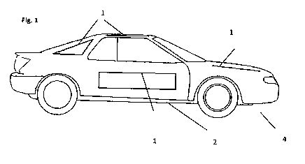
Fig. 1 shows a schematic diagram of an arrangement of films according to the
invention in the form of a package as part of a body of a vehicle,
Fig. 2 shows a schematic diagram of an arrangement of films according to the
invention in form of a coil in a lighting system.
According to Fig. 1 and Fig. 2, multiple films 1 according to the invention
are
arranged in layers in the form of a package. The films 1 themselves are, or
the at
least one film 1 itself is, part of a body 2, of a frame 3 according to Fig. 2
or of a
housing or other suitable component of a consumer unit of electric energy, an
energy
consumer 4. The film 1 according to the invention can be introduced, for
example
within the framework of a known hybrid construction, into a frame 3 or a body
2.
Date Recue/Date Received 2021-05-19

CA 03120538 2021-05-19
The energy consumer 4 in Fig. 1 is a vehicle and is a lighting system in Fig.
2. It can,
however, be any device operated with electric energy, in particular any
machine
operated with electric energy.
Date Recue/Date Received 2021-05-19

CA 03120538 2021-05-19
6
List of reference numerals:
1. Film
2. Body
3. Frame
4. Energy consumer
Date Recue/Date Received 2021-05-19

Representative Drawing
A single figure which represents the drawing illustrating the invention.
Administrative Status

2024-08-01:As part of the Next Generation Patents (NGP) transition, the Canadian Patents Database (CPD) now contains a more detailed Event History, which replicates the Event Log of our new back-office solution.

Please note that "Inactive:" events refers to events no longer in use in our new back-office solution.

For a clearer understanding of the status of the application/patent presented on this page, the site Disclaimer , as well as the definitions for Patent , Event History , Maintenance Fee  and Payment History  should be consulted.

Event History

Description Date
Compliance Requirements Determined Met 2022-12-05
Letter Sent 2022-09-20
Common Representative Appointed 2021-11-13
Inactive: Cover page published 2021-07-13
Letter sent 2021-06-15
Priority Claim Requirements Determined Compliant 2021-06-08
Application Received - PCT 2021-06-08
Inactive: First IPC assigned 2021-06-08
Inactive: IPC assigned 2021-06-08
Request for Priority Received 2021-06-08
National Entry Requirements Determined Compliant 2021-05-19
Application Published (Open to Public Inspection) 2020-05-28

Abandonment History

There is no abandonment history.

Maintenance Fee

The last payment was received on 2023-08-31

Note : If the full payment has not been received on or before the date indicated, a further fee may be required which may be one of the following

  • the reinstatement fee;
  • the late payment fee; or
  • additional fee to reverse deemed expiry.

Patent fees are adjusted on the 1st of January every year. The amounts above are the current amounts if received by December 31 of the current year.
Please refer to the CIPO Patent Fees web page to see all current fee amounts.

Fee History

Fee Type Anniversary Year Due Date Paid Date
Basic national fee - standard 2021-05-19 2021-05-19
MF (application, 2nd anniv.) - standard 02 2021-09-17 2021-09-09
MF (application, 3rd anniv.) - standard 03 2022-09-20 2022-12-05
Late fee (ss. 27.1(2) of the Act) 2022-12-05 2022-12-05
MF (application, 4th anniv.) - standard 04 2023-09-18 2023-08-31
Owners on Record

Note: Records showing the ownership history in alphabetical order.

Current Owners on Record
NEUTRINO DEUTSCHLAND GMBH
Past Owners on Record
HOLGER THORSTEN SCHUBART
Past Owners that do not appear in the "Owners on Record" listing will appear in other documentation within the application.
Documents

To view selected files, please enter reCAPTCHA code :


To view images, click a link in the Document Description column. To download the documents, select one or more checkboxes in the first column and then click the "Download Selected in PDF format (Zip Archive)" or the "Download Selected as Single PDF" button.

List of published and non-published patent-specific documents on the CPD .

If you have any difficulty accessing content, you can call the Client Service Centre at 1-866-997-1936 or send them an e-mail at CIPO Client Service Centre.


Document
Description 
Date
(yyyy-mm-dd) 
Number of pages   Size of Image (KB) 
Description 2021-05-18 6 213
Representative drawing 2021-05-18 1 6
Drawings 2021-05-18 1 10
Claims 2021-05-18 3 101
Abstract 2021-05-18 1 11
Courtesy - Letter Acknowledging PCT National Phase Entry 2021-06-14 1 587
Commissioner's Notice - Maintenance Fee for a Patent Application Not Paid 2022-10-31 1 550
Amendment - Abstract 2021-05-18 1 66
National entry request 2021-05-18 5 143
Declaration 2021-05-18 1 50
International search report 2021-05-18 4 129