Note: Descriptions are shown in the official language in which they were submitted.
CA 03120657 2021-05-20
WO 2020/106542 PCT/US2019/061462
NICKEL OXIDE SOL-GEL INK
[0001] This application claims priority to U.S. Provisional Patent Application
No.
62/770,389 filed November 21, 2018 and entitled "Nickel Oxide Sol-Gel Ink."
TECHNICAL FIELD
[0002] Particular embodiments relate generally to compositions for use in
photovoltaic
and optoelectronic devices, and more particularly to nickel oxide precursor
ink compositions for
use as thin film layers in photovoltaic, electronic, optoelectronic, and
mechanical devices.
BACKGROUND
[0003] Photovoltaic (PV) and optoelectronic devices comprise multi-layer
structures.
Conventional precursor ink formulations for nickel oxide thin films among
multiple layers in the
PV devices have yielded incomplete surface coverage, poor surface morphology
and undesirable
optoelectronic properties. In perovskite photovoltaics, incomplete surface
coverage can lead to
increased non-radiative recombination and reduced open-circuit voltage. Poor
surface
morphology can negatively impact the perovskite film growth and quality.
[0004] Nickel oxide has been known to serve as a hole-transport and/or
electron-blocking
layer in PV and optoelectronic devices. Previous demonstrations of nickel
oxide precursor inks
often resulted in incomplete surface coverage, poor film morphology, and/or
undesirable
optoelectronic properties.
SUMMARY
[0005] To address the foregoing problems with existing solutions, disclosed is
a nickel
oxide (NiO) precursor ink.
[0006] According to some embodiments, a composition for use in a preparation
of a
nickel oxide layer includes nickel nitrate (Ni(NO3)2.nH20, wherein n is 0, 4,
6 or 9), at least one
metal acetate; and a solvent combination comprising a diol, an alcohol amine,
and water.
[0007] In particular embodiments, the at least one metal acetate is selected
from the
group of: nickel acetate tetrahydrate, copper acetate monohydrate, and
combinations thereof
1
CA 03120657 2021-05-20
WO 2020/106542 PCT/US2019/061462
[0008] In particular embodiments, the solvent combination comprises ethylene
glycol,
ethanolamine, and water.
[0009] In particular embodiments, the solvent combination comprises ethylene
glycol,
ethanolamine, water and acetylacetone.
[0010] In particular embodiments, the at least one metal acetate comprises
nickel acetate
tetrahydrate.
[0011] In particular embodiments, wherein the at least one metal acetate
comprises
copper acetate monohydrate.
[0012] In particular embodiments, the at least one metal acetate comprises
nickel acetate
tetrahydrate and copper acetate monohydrate.
[0013] According to some embodiments, a method for preparing a nickel oxide
precursor
ink includes: first, preparing a solvent comprising diols and alcohol amines.
Next, adding nickel
nitrate into the solvent to form a nickel nitrate containing solution. Next,
adding at least one
metal acetate into the nickel nitrate containing solution to form a nickel
nitrate and metal acetate
containing solution. Next, adding water to the nickel nitrate and metal
acetate containing solution
to form a nickel oxide precursor mixture. Next, heating the nickel oxide
precursor mixture to 60
to 75 Celsius. Finally, cooling the nickel oxide precursor mixture to form the
nickel oxide
precursor ink.
[0014] In particular embodiments, the nickel nitrate is Ni(NO3)2.nH20 and n is
0, 4, 6 or
9.
[0015] In particular embodiments, the metal acetate is Ni(CH3CO2)2.xH20, and x
is 0, 2
or 4.
[0016] In particular embodiments, the nickel nitrate is Ni(NO3)2.6H20 and the
at least
one metal acetate is Ni(CH3CO2)2.4H20.
[0017] In particular embodiments, the at least one metal acetate comprises
Ni(CH3CO2)2.xH20 and Cu(CH3CO2)2.bH20, wherein x is 0, 2 or 4 and b is 0 or 1.
[0018] In particular embodiments, the nickel nitrate is Ni(NO3)2.6H20 and the
at least
one metal acetate comprises Ni(CH3CO2)2.4H20 and Cu(CH3CO2)2.1H20.
[0019] In particular embodiments, the nickel oxide precursor mixture has a
concentration
of Ni(NO3)2.6H20 is between 0.7 M and 0.8 M and a concentration of
Ni(CH3CO2)2.4H20 is
between 50 mM and 110 mM.
2
CA 03120657 2021-05-20
WO 2020/106542 PCT/US2019/061462
[0020] In particular embodiments, the concentration of Ni(NO3)2.6H20 is 0.72 M
and the
concentration of Ni(CH3CO2)2.4H20 is 103 mM.
[0021] In particular embodiments, the nickel oxide precursor mixture has a
concentration
of Ni(NO3)2.6H20 between 0.7 M and 0.8 M, a concentration of Ni(CH3CO2)2.4H20
between 50
mM and 110 mM, and a concentration of Cu(CH3CO2)2.1H20 between 20 mM and 41.3
mM.
[0022] In particular embodiments, the solvent comprises ethylene glycol and
ethanolamine.
[0023] In particular embodiments, the solvent comprises ethylene glycol and
ethanolamine; and the ethylene glycol, ethanolamine and water have a volume
ratio of 12:1.46:1,
respectively.
[0024] In particular embodiments, the method is performed under an inert
atmosphere
having less than 5ppm water and less than 5ppm oxygen.
[0025] According to some embodiments, a method for depositing a nickel oxide
layer
includes: first, preparing a substrate. Next, depositing a nickel oxide
precursor ink onto the
substrate. The nickel oxide precursor ink includes a solvent comprising diols,
alcohol amines,
and water, Ni(NO3)2.6H20, and at least one metal acetate selected from the
group consisting of
Ni(CH3CO2)2.4H20 and Cu(CH3CO2)2.1H20. Next, annealing the nickel oxide
precursor ink at
a temperature between 250 to 400 Celsius for between 10 minutes and 6 hours.
Finally, cooling
the nickel oxide precursor ink to form the nickel oxide layer.
[0026] In particular embodiments, the method further includes filtering the
nickel oxide
precursor ink prior to depositing the nickel oxide precursor ink onto the
substrate.
[0027] In particular embodiments, the solvent comprises ethylene glycol,
ethanolamine
and water.
[0028] In particular embodiments, the substrate is selected from the group
consisting of
glass, p-doped silicon, n-doped silicon, sapphire, magnesium oxide, mica,
polymers, ceramics,
fabrics, wood, drywall, metal, or combinations thereof, and any of the
forgoing materials coated
with materials selected from the group consisting of indium-doped tin oxide
(ITO), fluorine-
doped tin oxide (FTO), cadmium oxide (CdO), zinc indium tin oxide (ZITO),
aluminum zinc
oxide (AZO), aluminum (Al), gold (Au), calcium (Ca), magnesium (Mg), titanium
(Ti), iron (Fe),
chromium (Cr), copper (Cu), silver (Ag), nickel (Ni), tungsten (W), molybdenum
(Mo), carbon
allotropes, or combinations thereof.
3
CA 03120657 2021-05-20
WO 2020/106542 PCT/US2019/061462
[0029] In particular embodiments, the method is performed under an environment
having
a humidity between 10% and 50% and a temperature between 200 and 60 Celsius.
[0030] In particular embodiments, annealing takes place at a temperature of
310 Celsius
for a time period of two hours.
[0031] According to certain embodiments, a composition for use in a
preparation of a
nickel oxide layer includes at least one metal nitrate, at least one metal
acetate, and a solvent
combination comprising a diol, an alcohol amine, and water.
[0032] In particular embodiments, the least one metal nitrate comprises copper
nitrate,
the at least one metal acetate comprises nickel acetate; the solvent comprises
ethylene glycol,
ethanolamine, and water.
[0033] In particular embodiments, wherein the least one metal nitrate
comprises nickel
nitrate, the at least one metal acetate comprises copper acetate, and the
solvent comprises
ethylene glycol, ethanolamine, and water.
[0034] In particular embodiments, wherein the least one metal nitrate
comprises nickel
nitrate, the at least one metal acetate comprises nickel acetate, and the
solvent comprises
ethylene glycol, ethanolamine, and water.
[0035] In particular embodiments, wherein: the least one metal nitrate
comprises nickel
nitrate, the at least one metal acetate comprises nickel acetate and copper
acetate, and the solvent
comprises ethylene glycol, ethanolamine, and water.
[0036] Nickel oxide precursor inks disclosed herein may be deposited via
solution-based
inks or physical deposition methods, such as spin coating, blade coating, and
slot-die coating.
Nickel oxide precursor inks disclosed herein also provide tunability through
the ink formulation
and additive engineering. Solution-based nickel oxide precursor inks disclosed
herein enable
high-throughput, low-cost deposition techniques. In addition, increasing the
transparency of the
layer/film prepared from nickel oxide precursor inks disclosed herein can
reduce parasitic
absorption and increase the short-circuit current. Alternatively, increasing
the absorption of
higher energy photons may be used as filtering for UV-induced degradation. The
formulation of
nickel oxide precursor inks disclosed herein provides the optionality for
different applications.
[0037] The features and advantages of the present disclosure will be readily
apparent to
those skilled in the art. While numerous changes may be made by those skilled
in the art, such
changes are within the spirit of the invention.
4
CA 03120657 2021-05-20
WO 2020/106542 PCT/US2019/061462
BRIEF DESCRIPTION OF THE DRAWINGS
[0038] FIGURE 1 is an example diagram illustrating components of an exemplar
PV
device according to some embodiments of the present disclosure.
[0039] FIGURE 2 is another example diagram illustrating components of an
exemplar
PV device according to some embodiments of the present disclosure.
[0040] FIGURE 3 is a stylized diagram illustrating components of an exemplar
PV
device according to some embodiments of the present disclosure.
[0041] FIGURE 4 is another stylized diagram illustrating components of an
exemplar PV
device according to some embodiments of the present disclosure.
[0042] FIGURE 5 is another stylized diagram illustrating components of an
exemplar PV
device according to some embodiments of the present disclosure.
[0043] FIGURE 6 illustrates SEM (scanning electron microscope) photos of an
example
NiO layer from the prior art.
[0044] FIGURE 7A illustrates an SEM photo of an example NiO layer, taken at
20,000X
magnification, according to some embodiments of the present disclosure.
[0045] FIGURE 7B illustrates an SEM photo of an example NiO layer, taken at
50,000X
magnification, according to some embodiments of the present disclosure.
[0046] FIGURE 7C illustrates SEM photos of an example NiO layer, taken at
200,000X
magnification, according to some embodiments of the present disclosure.
[0047] FIGURE 8A illustrates an SEM photo of another example NiO layer, taken
at
5,000X magnification, according to some embodiments of the present disclosure.
[0048] FIGURE 8B illustrates an SEM photo of another example NiO layer, taken
at
20,000X magnification, according to some embodiments of the present
disclosure.
[0049] FIGURE 8C illustrates an SEM photo of another example NiO layer, taken
at
50,000X magnification, according to some embodiments of the present
disclosure.
[0050] FIGURE 8D illustrates an SEM photo of another example NiO layer, taken
at
200,000X magnification, according to some embodiments of the present
disclosure.
[0051] FIGURE 8E illustrates SEM photos of another example NiO layer, taken at
150,000X magnification, according to some embodiments of the present
disclosure.
CA 03120657 2021-05-20
WO 2020/106542 PCT/US2019/061462
[0052] FIGURE 9A illustrates an SEM photo of another example NiO layer, taken
at
20,000X magnification, according to some embodiments of the present
disclosure.
[0053] FIGURE 9B illustrates an SEM photo of another example NiO layer, taken
at
50,000X magnification, according to some embodiments of the present
disclosure.
[0054] FIGURE 9C illustrates an SEM photo of another example NiO layer, taken
at
150,000X magnification, according to some embodiments of the present
disclosure.
[0055] FIGURE 10A illustrates an SEM photo of another example NiO layer, taken
at
20,000X magnification, according to some embodiments of the present
disclosure.
[0056] FIGURE 10B illustrates an SEM photo of another example NiO layer, taken
at
50,000X magnification, according to some embodiments of the present
disclosure.
[0057] FIGURE 10C illustrates an SEM photo of another example NiO layer, taken
at
150,000X magnification, according to some embodiments of the present
disclosure.
[0058] FIGURE 11A illustrates an SEM photo of yet another example NiO layer,
taken
at 20,000X magnification, according to some embodiments of the present
disclosure.
[0059] FIGURE 11B illustrates an SEM photo of another example NiO layer, taken
at
50,000X magnification, according to some embodiments of the present
disclosure.
[0060] FIGURE 11C illustrates an SEM photo of another example NiO layer, taken
at
150,000X magnification, according to some embodiments of the present
disclosure.
[0061] FIGURE 12 is an UV-Visible absorptance diagram of NiO and perovskite on
NiO
layers according to some embodiments of the present disclosure.
[0062] FIGURE 13 is a photoluminescence diagram of perovskite on NiO layers
according to some embodiments of the present disclosure.
[0063] FIGURE 14 is Fourier-transform infrared spectroscopy of NiO layers
according to
some embodiments of the present disclosure.
[0064] FIGURE 15 is an example film stack including NiO layer according to
some
embodiments of the present disclosure.
[0065] FIGURE 16 is another example film stack including NiO layer according
to some
embodiments of the present disclosure.
6
CA 03120657 2021-05-20
WO 2020/106542 PCT/US2019/061462
DETAILED DESCRIPTION OF PREFERRED EMBODIMENTS
[0066] The present disclosure relates generally to materials to form a thin
film layer,
methods of preparing and applying the materials to thin film layer, and
apparatus of use of thin
film layer in optical devices, electronic devices, mechanical devices, and
photovoltaic cells in
increasing short-circuit current and open-circuit voltage, and reducing
parasitic absorption.
More specifically, this disclosure relates to formation of nickel oxide (NiO)
precursor ink
compositions, as well as apparatus, methods of use, and preparation of such
compositions of
matter.
[0067] The NiO precursor ink of the present disclosure includes a nickel
nitrate and/or
nickel acetate and may include a metal nitrate or metal acetate dissolved in a
solvent mixture
comprising a diol, water, and an alcohol-amine. In some embodiments the NiO
precursor ink
includes nickel nitrate an one or more metal acetates dissolved in a solvent
mixture comprising a
diol, water, and an alcohol. In other embodiments, the NiO precursor ink
includes nickel acetate
and one or more metal nitrates, and does not include nickel nitrate, dissolved
in a solvent mixture
comprising a diol, water, and an alcohol-amine. After the NiO precursor ink
layer has been
deposited on a substrate, the layers and/or films may be heated and annealed,
resulting in a
combustion reaction that yields a nickel oxide thin layer/film which is formed
by the NiO
precursor ink disclosed in the present disclosure. The yielded nickel oxide
thin layer/film may
serve as an effective hole-transport layer in photovoltaic devices.
[0068] In some embodiments, the NiO precursor ink of the present disclosure
may
include other metals as described herein. These metals may act as dopants in
the resulting nickel
oxide thin film, resulting in hole-transporting or electron-transporting
nickel oxide thin films,
depending on the metal dopant(s) included in the NiO precursor ink.
[0069] Examples of compounds to prepare the NiO precursor ink may include, but
are
not limited to, anhydrous nickel nitrate, nickel nitrate hexahydrate, nickel
nitrate nonahydrate,
nickel nitrate tetrahydrate, nickel nitrate dihydrate, and any derivative
hydrates of nickel nitrate,
and anhydrous nickel acetate, nickel acetate dihydrate, nickel acetate
tetrahydrate, and anhydrous
copper nitrate, copper nitrate monohydrate, copper nitrate sesquihydrate,
copper nitrate
hemipentahydrate, copper nitrate trihydrate, copper nitrate hexahydrate, and
any derivative
hydrates of copper nitrate, and anhydrous copper acetate, copper acetate
monohydrate.
7
CA 03120657 2021-05-20
WO 2020/106542 PCT/US2019/061462
[0070] The NiO precursor inks of the present disclosure may be formulated
using a
mixture of nickel nitrate (Ni(NO3)2), a metal acetate, and water in a diol
solvent with an alcohol-
amine additive. In certain embodiments, the metal acetate may be one or more
of nickel acetate
(Ni(CH3CO2)2) or copper acetate (Cu(CH3CO2)2), and amines, diamines, and
acetylacetone (and
derivatives thereof) may also be included in the NiO precursor ink.
Compositions and methods
for forming embodiments of the NiO precursor ink are described further herein.
After the NiO
precursor ink is formulated, it may be deposited and annealed to form a NiO
thin film. The
resulting NiO thin film may be a p-type semiconductor. In some embodiments,
the NiO
precursor ink may be applied to form an NiO thin film in a variety of
electronic devices,
including but not limited to photovoltaics (PV), field effect transistors
(FETs), light emitting
diodes (LEDs), charge coupled devices (CCDs), photodiodes, x-ray detectors,
and
complementary metal¨oxide¨semiconductors (CMOS).
[0071] In some embodiments, a nickel oxide precursor ink may be formulated
with a
mixture of nickel nitrate, nickel acetate, water, and ethanol amine in an
ethylene glycol solvent.
In other embodiments, a nickel oxide precursor ink may be formulated with a
mixture of nickel
nitrate, nickel acetate, water, ethanol amine, and acetylacetone in an
ethylene glycol solvent. In
yet other embodiments, a nickel oxide precursor ink may be formulated with a
mixture of nickel
nitrate, copper acetate, water, and ethanol amine in an ethylene glycol
solvent. In yet other
embodiments, a nickel oxide precursor ink may be formulated with a mixture of
nickel nitrate,
copper acetate, water, ethanol amine, and acetylacetone in an ethylene glycol
solvent. In other
embodiments, a nickel oxide precursor ink may be formulated with a mixture of
nickel nitrate, a
metal acetate having the formula M(CH3CO2)y wherein M may be any metal (for
example, Cu,
Li, Na, K, Rb, Cs, Be, Mg, Ca, Sr, Ba, Sc, Y, Ti, Zr, Hf, V, Nb, Ta, Cr, Mo,
W, Mn, Re, Fe, Ru,
Os, Co, Rh, Ii, Pd, Pt, Cu, Ag, Au, Zn, Cd, Hg, B, Al, Ga, In, Tl, Si, Ge, Sn,
Pb, As, Sb, Bi, Se,
Te, La, Ce, Pr, Nd, Sm, Er, Gd, Tb, Dy, Ho, Er, Ym, Yb, Lu, Ac, Th, Pa, and U)
and y
corresponds to the oxidation state of the metal M (e.g., y=2 where M is Cu'
and y=6 where M is
W6+), water, and ethanol amine in an ethylene glycol solvent.
[0072] In some embodiments, hydrates of nickel nitrate (e.g., Ni(NO3)2.aH20),
nickel
acetate (e.g., Ni(CH3CO2)2.bH20), copper acetate (e.g., Cu(CH3CO2)2.cH20), or
metal acetate
(e.g., M(CH3CO2)y.dH20) may be included in the nickel oxide precursor ink
formulation as
8
CA 03120657 2021-05-20
WO 2020/106542 PCT/US2019/061462
described herein, where a, b, c, and d in the forgoing formulas correspond to
a number of H20
molecules in the hydrate.
[0073] In some embodiments, compounds for preparing the NiO precursor inks may
include nickel nitrate hexahydrate (Ni(NO3)2.6H20), nickel acetate
tetrahydrate
(Ni(CH3CO2)2.4H20), copper nitrate trihydrate (Cu(NO3)2.3H20), and copper
acetate
monohydrate (Cu(CH3CO2)2. H20).
[0074] Examples of solvents for preparing the NiO precursor ink may include,
but are not
limited to, one or more of glycerol; ethylene glycol; propylene glycol;
methanol; ethanol; and
any other compounds comprising at least one hydroxyl groups, such as alcohols
and diols;
ammonia; acetone; acetylacetone, and any compounds comprising at least one
carbonyl group;
ethylamine, and any other aryl and alkylamines; ethanolamine, and any amines
comprising at
least one hydroxyl group; water; di- and polyamines, and any other solvent
suitable to dissolve
the compounds for preparing the NiO precursor ink.
[0075] In certain embodiments, a solvent for preparing the NiO precursor inks
may
comprise ethylene glycol, ethanolamine and water. In one particular
embodiment, the solvent
may comprise ethylene glycol, ethanolamine and water in a ratio of 12:1.46:1
by volume.
[0076] In a particular embodiment, the NiO precursor ink consists of Ni(NO3)2
and
Ni(CH3CO2)2 dissolved in a solvent mixture consisting of a diol, an alcohol
amine, and water.
[0077] In another embodiment, the NiO precursor ink consists of Ni(NO3)2 and a
metal
acetate (M(CH3CO2)y) dissolved in a solvent mixture consisting of a diol, an
alcohol amine, and
water.
[0078] In another embodiment, the NiO precursor ink consists of Ni(NO3)2,
Ni(CH3CO2)2 and a metal acetate (M(CH3CO2)y) dissolved in a solvent mixture
consisting of a
diol, an alcohol amine, and water.
[0079] In another embodiment, the NiO precursor ink consists of Ni(NO3)2,
Ni(CH3CO2)2 and a metal nitrate (M(NO3)y) dissolved in a solvent mixture
consisting of a diol,
an alcohol amine, and water.
[0080] In another embodiment, the NiO precursor ink consists of Ni(CH3CO2)2,
and a
metal nitrate (M(NO3)y) dissolved in a solvent mixture consisting of a diol,
an alcohol amine,
and water.
9
CA 03120657 2021-05-20
WO 2020/106542 PCT/US2019/061462
[0081] An example preparation of the NiO precursor ink may comprise 0.7-0.8 M
nickel
nitrate hexahydrate and 50-110 mM nickel acetate tetrahydrate in a solvent
which comprises
ethylene glycol, ethanolamine and water in a volume ratio of 5-20 to 1-5 to 1-
5, respectively. In
a particular embodiment, the preparation of the NiO precursor ink may comprise
0.72 M nickel
nitrate hexahydrate and 103 mM nickel acetate tetrahydrate in a solvent which
comprises
ethylene glycol, ethanolamine and water in a volume ratio of 12:1.46:1. In
some embodiments,
the NiO precursor ink may additionally include 0-20 mol% copper and 0-50 mol%
acetate.
[0082] Another example preparation of the NiO precursor ink may comprise 0.7-
0.8 M
nickel nitrate and50-110 mM metal acetate in a solvent which comprises
ethylene glycol,
ethanolamine and water in a volume ratio of 5-20 to 1-5 to 1-5, respectively.
In a particular
embodiment, the preparation of the NiO precursor ink may comprise 0.72 M
nickel nitrate
hexahydrate and 103 mM metal acetate in a solvent which comprises ethylene
glycol,
ethanolamine and water in a volume ratio of 12:1.46:1. In some embodiments,
the NiO
precursor ink may additionally include 0-20 mol% copper and 0-50 mol% acetate.
[0083] Another example preparation of the NiO precursor ink may comprise 0.7-
0.8 M
nickel nitrate hexahydrate, 50-110 mM nickel acetate tetrahydrate, and 20-41.3
mM metal
nitrate in a solvent which comprises ethylene glycol, ethanolamine and water
in a volume ratio of
5-20 to 1-5 to 1-5, respectively. In a particular embodiment, the metal
nitrate may be copper
nitrate trihydrate. In a particular embodiment, the preparation of the NiO
precursor ink may
comprise 0.72 M nickel nitrate hexahydrate, 103 mM nickel acetate
tetrahydrate, and 30 mM
metal nitrate in a solvent which comprises ethylene glycol, ethanolamine and
water in a volume
ratio of 12:1.46:1.
[0084] Another example preparation of the NiO precursor ink may comprise 0.7-
0.8 M
nickel nitrate hexahydrate, 50-110 mM nickel acetate tetrahydrate, and 20-41.3
mM metal
acetate in a solvent which comprises ethylene glycol, ethanolamine and water
in a volume ratio
of 5-20 to 1-5 to 1-5, respectively. In some embodiments, the metal nitrate
may be copper
acetate. In a particular embodiment, the preparation of the NiO precursor ink
may comprise 0.72
M nickel nitrate hexahydrate, 103 mM nickel acetate tetrahydrate, and 30 mM
metal acetate in a
solvent which comprises ethylene glycol, ethanolamine and water in a volume
ratio of 12:1.46:1.
[0085] Another example preparation of the NiO precursor ink may comprise 0.7-
0.8 M
metal nitrate and 50-110 mM nickel acetate tetrahydrate in a solvent which
comprises ethylene
CA 03120657 2021-05-20
WO 2020/106542 PCT/US2019/061462
glycol, ethanolamine and water in a volume ratio of 5-20 to 1-5 to 1-5,
respectively. In a
particular embodiment, the preparation of the NiO precursor ink may comprise
0.72 M metal
nitrate and 103 mM nickel acetate tetrahydrate in a solvent which comprises
ethylene glycol,
ethanolamine and water in a volume ratio of 12:1.46:1.
[0086] An example method for preparing the NiO may include, but is not limited
to, the
following steps. First, a solvent is prepared comprising diols and amines
which comprise at least
one hydroxyl group (an "alcohol-amine"). For example, the solvent may be
prepared by mixing
ethanolamine into ethylene glycol. Next, Ni(NO3)2.aH20 is added to the
solvent, where a may be
0, 4, 6 or 9. In particular embodiments, the nickel nitrate may be nickel
nitrate hexahydrate (a =
6). Next, Ni(CH3CO2)2.bH20 is added to the mixture, where b may be 0, 2, or 4.
The nickel
acetate may be nickel acetate tetrahydrate, in particular embodiments. Next,
water is added to the
mixture. Next, the mixture is heated.. Finally, the mixture is cooled to form
the NiO precursor
ink. In certain embodiments, when each component is added to the mixture, the
mixture may be
mixed by vibrating, agitating, stirring, homogenizing, combining turbulent
flows, vortex mixing,
or any other known method of mixing. In certain embodiments, the NiO layer may
be prepared
in either an inert atmosphere or an atmosphere having a high humidity (e.g.
greater than 4 grams
H20 per liter of the atmosphere).
[0087] In some embodiments, water may be added before the cooling step, so
that the
final concentration of nickel nitrate hexahydrate is 0.7-0.8 M and the final
concentration of
nickel acetate tetrahydrate is 50-110 mM.
[0088] The NiO precursor ink may be deposited onto a variety of substrates to
form a
thin film NiO layer for use in optical, mechanical, and electronic
applications, including but not
limited to photovoltaics (PV), field effect transistors (FETs), light emitting
diodes (LEDs),
charge coupled devices (CCDs), photodiodes, x-ray detectors, and complementary
metal¨oxide¨
semiconductors (CMOS). In some embodiments, the layer formed by the NiO
precursor ink may
be used in photovoltaic cells. In particular embodiments, the layer formed by
the NiO precursor
ink may be used as hole-transport and/or electron-transport layers. In certain
embodiments, the
NiO precursor ink maybe deposited as a thin-film IFL. In particular
embodiments, the NiO
precursor ink may be deposited to form a thin film NiO layer in a photovoltaic
device with a
perovskite photoactive layer.
11
CA 03120657 2021-05-20
WO 2020/106542 PCT/US2019/061462
[0089] Suitable substrate materials include any one or more of: glass; quartz,
p-doped
silicon substrate; n-doped silicon substrate; sapphire; magnesium oxide (MgO);
mica; polymers
(e.g., PET, PEG, PES, polypropylene, polyethylene, etc.); ceramics; fabrics
(e.g., cotton, silk,
wool); wood; drywall; metal; and combinations thereof. In some embodiments,
the substrate
onto which the NiO precursor ink may be deposited may be coated with an
electrode. The
electrode may be either an anode or a cathode. Suitable materials for the
electrode may include
indium-doped tin oxide (ITO); fluorine-doped tin oxide (FT0); cadmium oxide
(CdO); zinc
indium tin oxide (ZITO); aluminum zinc oxide (AZO); aluminum (Al); gold (Au);
calcium (Ca);
magnesium (Mg); titanium (Ti); iron (Fe); chromium (Cr); copper (Cu); silver
(Ag); nickel (Ni);
tungsten (W); molybdenum (Mo); carbon (and allotropes thereof); and
combinations thereof, and
any other materials which may function as an electrode. For example, the
substrate with
electrode coating may include ITO-coated glass, FTO-coated glass, Ag-coated
glass, CdO-coated
glass, and ITO-coated PET.
[0090] In some embodiments the substrate may be additionally coated with one
or more
interfacial layers (IFL) as described herein. In some embodiments, the IFL may
be alumina
(Al2O3). In some embodiments, the IFL may form a contiguous layer. In other
embodiments, the
IFL may form a non-contiguous layer.
[0091] An example method for depositing the NiO precursor ink may include, but
is not
limited to, preparing a substrate, depositing the NiO precursor ink onto the
substrate, annealing
the NiO precursor ink and cooling the NiO precursor ink to form a thin film
NiO layer.
Depositing the NiO precursor ink onto the substrate may include depositing the
NiO precursor
ink onto any preceding layers deposited onto the substrate. For example, an
electrode layer may
be deposited onto the substrate prior to deposition of the NiO precursor ink,
which may then be
deposited onto the electrode layer. Likewise, in some embodiments, an
electrode layer and one
or more interfacial layers may be deposited onto the substrate prior to
deposition of the NiO
precursor ink.
[0092] In some embodiments, depositing the NiO precursor ink may be performed
by
spin coating, blade coating, slot-die coating, screen printing, roll-to-roll
coating, spray coating,
dip coating, or gravure printing. In some embodiments, the NiO precursor ink
may be deposited
onto the substrate in an environment having a relative humidity between 10 and
50% and a
temperature between 20 and 60 Celsius. In a particular embodiment, the NiO
precursor ink
12
CA 03120657 2021-05-20
WO 2020/106542 PCT/US2019/061462
may be deposited onto the substrate in an environment having a relative
humidity of 35% and a
temperature of 35 Celsius. In some embodiments, the NiO precursor ink may be
filtered before
being deposited onto the substrate. In particular embodiments, filtering the
NiO precursor ink
may include dispensing the NiO precursor ink through 0.2 p.m filter. In some
embodiments,
annealing may take place at a temperature between 250 Celsius and 400
Celsius for a time
period between 30 minutes and 6 hours. In a particular embodiment, annealing
may take place at
a temperature of 310 Celsius for a time period of two hours. In some
embodiments, the step of
annealing the IFL on the substrate may include increasing the temperature from
35 to 310
Celsius at a rate of approximately 50 Celsius per five minutes. Cooling the
NiO thin film layer
formed after annealing the NiO precursor ink may include cooling it to near-
room temperature
(20 ¨ 50 Celsius) by allowing the substrate and thin film layers to rest
in a near-room
temperature environment. In some embodiments, the NiO thin film layer may
annealed one or
more times after the first annealing step, in the same manner as described
above. For example, a
substrate with an NiO thin film layer deposited as disclosed herein may be
stored and reannealed
prior to subsequent processing steps.
[0093] In a particular embodiment, the method for depositing the NiO precursor
ink may
include preparing a substrate, depositing an alumina thin film layer,
depositing the NiO precursor
ink onto the alumina thin film, annealing the NiO precursor ink to form a NiO
thin film,
depositing a perovskite material, depositing an interfacial layer, and
depositing an electrode. In
some embodiments, depositing the NiO precursor ink may follow a pattern which
starts at one
side of the substrate and covers the substrate row by row continuously to
ensure a good coverage
of NiO precursor ink on the substrate without dripping.
[0094] FIG. 1 illustrates a stylized diagram of a perovskite material device
1000
according to some embodiments. Although various components of the device 1000
are
illustrated as discrete layers comprising contiguous material, it should be
understood that FIG. 1
is a stylized diagram; thus, embodiments in accordance with it may include
such discrete layers,
and/or substantially intermixed, non-contiguous layers, consistent with the
usage of "layers"
previously discussed herein. The device 1000 includes first and second
substrates 1010 and
1070. A first electrode 1020 is disposed upon an inner surface of the first
substrate 1010, and a
second electrode 1060 is disposed on an inner surface of the second substrate
1070. An active
layer 1100 is sandwiched between the two electrodes 1020 and 1060. The active
layer 1100
13
CA 03120657 2021-05-20
WO 2020/106542 PCT/US2019/061462
includes an interfacial layer (IFL) 1030; photoactive material (PAM) layer
1040; and an IFL
1050.
[0095] A perovskite material device according to some embodiments may
optionally
include one or more substrates. In some embodiments, either or both of the
first and second
electrodes 1020 and 1060 may be coated or otherwise disposed upon a substrate,
such that the
electrode is disposed substantially between a substrate and the active layer.
The materials of
composition of devices (e.g., substrate, electrode, active layer and/or active
layer components)
may in whole or in part be either rigid or flexible in various embodiments. In
some
embodiments, an electrode may act as a substrate, thereby negating the need
for a separate
substrate.
[0096] A substrate, such as either or both of first and second substrates 1010
and 1070,
may be flexible or rigid. If two substrates are included, at least one should
be transparent or
translucent to electromagnetic (EM) radiation (such as, e.g., UV, visible, or
IR radiation). If one
substrate is included, it may be similarly transparent or translucent,
although it need not be, so
long as a portion of the device permits EM radiation to contact the active
layer 1100.
[0097] As previously noted, an electrode (e.g., one of electrodes 1020 and
1060 of FIG.
1) may be either an anode or a cathode. In some embodiments, one electrode may
function as a
cathode, and the other may function as an anode. Either or both electrodes
1020 and 1060 may
be coupled to leads, cables, wires, or other means enabling charge transport
to and/or from the
device 1000. An electrode may constitute any conductive material, and at least
one electrode
should be transparent or translucent to EM radiation, and/or be arranged in a
manner that allows
EM radiation to contact at least a portion of the active layer 1100.
[0098] The example NiO precursor inks described herein may be deposited by any
of the
methods described herein to form a NiO thin film layer as an interfacial layer
(IFL) or in addition
to other IFLs as described below. An interfacial layer may include any
suitable material for
enhancing charge transport and/or collection between adjacent layers or
materials; it may also
help prevent or reduce the likelihood of charge recombination once a charge
has been transported
away from one of the materials adjacent to the interfacial layer. An
interfacial layer may
additionally physically and electrically homogenize its substrates to create
or reduce variations in
substrate roughness, dielectric constant, adhesion, creation or quenching of
defects (e.g., charge
traps, surface states). Suitable interfacial materials may include any one or
more of: Ag; Al; Au;
14
CA 03120657 2021-05-20
WO 2020/106542 PCT/US2019/061462
B; Bi; Ca; Cd; Ce; Co; Cr; Cu; Fe; Ga; Ge; H; In; Mg; Mn; Mo; Nb; Ni; Pt; Sb;
Sc; Si; Sn; Ta;
Ti; V; W; Y; Zn; Zr; carbides of any of the foregoing metals (e.g., SiC, Fe3C,
WC, VC, MoC,
NbC); silicides of any of the foregoing metals (e.g., Mg2Si, 5r5i2, 5n25i);
oxides of any of the
foregoing metals (e.g., alumina, silica, titania, 5n02, ZnO, W03, V205, Mo03,
NiO, ZrO2,
Hf02), include transparent conducting oxides ("TCOs") such as indium tin
oxide, aluminum
doped zinc oxide (AZO), cadmium oxide (CdO), and fluorine doped tin oxide
(FT0); sulfides of
any of the foregoing metals (e.g., CdS, MoS2, 5n52); nitrides of any of the
foregoing metals (e.g.,
GaN, Mg3N2, TiN, BN, Si3N4); selenides of any of the foregoing metals (e.g.,
CdSe, FeS2,
ZnSe); tellurides of any of the foregoing metals (e.g., CdTe, TiTe2, ZnTe);
phosphides of any of
the foregoing metals (e.g., InP, GaP, GaInP); arsenides of any of the
foregoing metals (e.g.,
CoAs3, GaAs, InGaAs, NiAs); antimonides of any of the foregoing metals (e.g.,
AlSb, GaSb,
InSb); halides of any of the foregoing metals (e.g., CuCl, CuI, BiI3);
pseudohalides of any of the
foregoing metals (e.g., CuSCN, AuCN, Fe(SCN)2); carbonates of any of the
foregoing metals
(e.g., CaCO3, Ce2(CO3)3); functionalized or non-functionalized alkyl silyl
groups; graphite;
graphene; fullerenes; carbon nanotubes; any mesoporous material and/or
interfacial material
discussed elsewhere herein; and combinations thereof (including, in some
embodiments,
bilayers, trilayers, or multi-layers of combined materials). In some
embodiments, an interfacial
layer may include perovskite material. Further, interfacial layers may
comprise doped
embodiments of any interfacial material mentioned herein (e.g., Y-doped ZnO, N-
doped single-
wall carbon nanotubes). Interfacial layers may also comprise a compound having
three of the
above materials (e.g., CuTiO3, Zn2Sn04) or a compound having four of the above
materials (e.g.,
CoNiZn0). The materials listed above may be present in a planar, mesoporous or
otherwise
nano-structured form (e.g. rods, spheres, flowers, pyramids), or aerogel
structure.
[0099] In certain embodiments, an alumina IFL layer as described herein may be
deposited according to the following method. First an alumina precursor
solution may be
prepared. The alumina precursor solution may be prepared by dissolving
aluminum nitrate in a
mixture of butanol, chloroform, and methanol. In some embodiments the butanol,
chloroform,
and methanol solution may have a ratio of 1:1:1 by volume of butanol,
chloroform, and
methanol. In certain embodiments, aluminum nitrate may be dissolved in with
butanol,
chloroform, and methanol to form a solution having a concentration of 25 mM of
aluminum
nitrate.
CA 03120657 2021-05-20
WO 2020/106542 PCT/US2019/061462
[00100] Next, the alumina precursor solution may be deposited onto a
substrate.
Depositing the alumina precursor solution onto the substrate may include
depositing the alumina
precursor solution precursor ink onto any preceding layers deposited onto the
substrate. In some
embodiments, the alumina precursor solution may be deposited by spin coating,
slot die coating,
or blade coating, amongst others described herein. In particular embodiments,
the alumina
precursor solution may be deposited so as to result in a layer 1 nm to 100 nm
in thickness. In
another embodiment, the alumina precursor solution may be deposited at a
thickness of less than
1 nm. In some embodiments, the alumina precursor solution may be deposited in
a continuous
manner over the entire area of the substrate. In other embodiments, the
alumina precursor
solution may be deposited in a discontinuous manner such that the alumina
precursor solution
covers portions of the area of the substrate. After deposition, the alumina
precursor may be
annealed. To anneal the alumina precursor, the temperature of the substrate
may be increased to
310 Celsius over a 25-minute interval, and then held at 310 Celsius for 35
minutes. Annealing
the alumina precursor may occur in a controlled humidity environment. In some
embodiments,
the controlled humidity environment may be controlled to maintain a humidity
of 25% relative
humidity during deposition and annealing of the alumina oxide precursor. After
annealing, the
substrate may be allowed to cool to room temperature in ambient conditions.
After annealing
and cooling, the alumina precursor to form an alumina layer, subsequent layers
may be deposited
onto the alumina layer, such as an NiO layer by the methods described herein.
The alumina layer
may be continuous or discontinuous over the surface of the substrate.
[00101] Although referred to herein as NiO and/or nickel oxide, it
should be noted
that various ratios of nickel and oxygen may be used in forming nickel oxide.
Thus, although
some embodiments discussed herein are described with reference to NiO, such
description is not
intended to define a required ratio of nickel in oxygen. Rather, embodiments
may include any
one or more nickel-oxide compounds, each having an nickel oxide ratio
according to NiO,
where x may be any value, integer or non-integer, between approximately 1 and
100. In some
embodiments, x may be between approximately 1 and 3 (and, again, need not be
an integer).
Likewise, y may be any value, integer or non-integer, between 0.1 and 100. In
some
embodiments, y may be between 2 and 4 (and, again, need not be an integer). In
addition,
various crystalline forms of NiO y may be present in various embodiments, such
as alpha,
gamma, and/or amorphous forms.
16
CA 03120657 2021-05-20
WO 2020/106542 PCT/US2019/061462
[00102] Furthermore, although referred to herein as A1203 and/or
alumina, it
should be noted that various ratios of aluminum and oxygen may be used in
forming alumina.
Thus, although some embodiments discussed herein are described with reference
to A1203, such
description is not intended to define a required ratio of aluminum in oxygen.
Rather,
embodiments may include any one or more aluminum-oxide compounds, each having
an
aluminum oxide ratio according to AlxOy, where x may be any value, integer or
non-integer,
between approximately 1 and 100. In some embodiments, x may be between
approximately 1
and 3 (and, again, need not be an integer). Likewise, y may be any value,
integer or non-integer,
between 0.1 and 100. In some embodiments, y may be between 2 and 4 (and,
again, need not be
an integer). In addition, various crystalline forms of AlxOy may be present in
various
embodiments, such as alpha, gamma, and/or amorphous forms of alumina.
[00103] Additionally, any metal oxide referred to herein may have
various ratios of
metal and oxygen. Embodiments may include any one or more metal-oxide
compounds, each
having an metal oxide ratio according to MxOy, where x may be any value,
integer or non-integer,
between approximately 1 and 100. In some embodiments, x may be between
approximately 1
and 3 (and, again, need not be an integer). Likewise, y may be any value,
integer or non-integer,
between 0.1 and 100. In some embodiments, y may be between 2 and 4 (and,
again, need not be
an integer). In addition, various crystalline forms of MO y may be present in
various
embodiments, such as alpha, gamma, and/or amorphous forms of alumina.
[00104] Any interfacial material discussed herein may further
comprise doped
compositions. To modify the characteristics (e.g., electrical, optical,
mechanical) of an interfacial
material, a stoichiometric or non-stoichiometric material may be doped with
one or more
elements (e.g., Na, Y, Mg, N, P) in amounts ranging from as little as 1 ppb to
50 mol %. Some
examples of interfacial materials include: NiO, TiO2, SrTiO3, A1203, ZrO2,
W03, V205, M03,
ZnO, graphene, and carbon black. Examples of possible dopants for these
interfacial materials
include: Be, Mg, Ca, Sr, Ba, Sc, Y, Nb, Ti, Fe, Co, Ni, Cu, Ga, Sn, In, B, N,
P, C, S, As, a halide,
a pseudohalide (e.g., cyanide, cyanate, isocyanate, fulminate, thiocyanate,
isothiocyanate, azide,
tetracarbonylcobaltate, carbamoyldicyanomethanide, dicyanonitrosomethanide,
dicyanamide,
and tricyanomethanide), and Al in any of its oxidation states. References
herein to doped
interfacial materials are not intended to limit the ratios of component
elements in interfacial
material compounds.
17
CA 03120657 2021-05-20
WO 2020/106542 PCT/US2019/061462
[00105]
Photoactive material 1040 may comprise any photoactive compound, such
as any one or more of silicon (in some instances, single-crystalline silicon),
cadmium telluride,
cadmium sulfide, cadmium selenide, copper indium gallium selenide, gallium
arsenide,
germanium indium phosphide, one or more semiconducting polymers, and
combinations thereof.
In some embodiments, photoactive material 1040 may include one or more
perovskite materials.
Perovskite materials include compositions having the formula CMX3, where C is
a cation, M is a
metal cation and X is an anion. In some embodiments, perovskite materials may
deviate from
the strict stoichiometry represented as CMX3 and include both
substoichiometric and
superstoichiometric compositions. Such perovskites may be represented by the
formula CxMyX,
where x, y, and z are real numbers. In some embodiments, solid perovskite-
containing material
may be deposited by any suitable means (e.g., vapor deposition, solution
deposition, direct
placement of solid material, etc.). Devices according to various embodiments
may include one,
two, three, or more photoactive compounds (e.g., one, two, three, or more
perovskite materials).
In certain embodiments, photoactive material 1040 may include MAPbI3, FAPbI3,
5-
AVA.HC1:FAPbI3, CHP:FAPbI3, Cs:FAPbI3, FA:MA:CsPbI3.yBry, CsPbI3, and/or
FA:MAPbI3,
where MA is methylammonium, FA is formamidinium, 5-AVA is 5-aminovaleric acid,
and CHP
is N-cyclohexy1-2-pyrrolidone. Additionally, photoactive material 1040 may
include both
substoichiometric and superstoichiometric compositions of the preceding
perovskite materials.
In embodiments including multiple photoactive materials, each of the
photoactive materials may
be separated by one or more interfacial layers. For example, FIG. 2
illustrates a stylized diagram
of a perovskite material device 2000, according to some embodiments.
The device 2000
includes first and second substrates 2010 and 2090. A first electrode 2020 is
disposed upon an
inner surface of the first substrate 2010, and a second electrode 2080 is
disposed on an inner
surface of the second substrate 2070. An active layer 2100 is sandwiched
between the two
electrodes 2020 and 2080. The active layer 2100 includes an IFL 2030;
photoactive materials
(PAM) layer 2040; IFL 2050 and 2055; PAM layer 2060 and IFL 1070. In some
embodiments
PAM layers 2040 and 2060 may be composed of different photoactive materials
which are
photoactive in response to different wavelengths of light.
[00106]
Charge transport material (e.g., a charge transport material of charge
transport layer 3050 in FIG. 3) may include solid-state charge transport
material (i.e., a
colloquially labeled solid-state electrolyte), or it may include a liquid
electrolyte and/or ionic
18
CA 03120657 2021-05-20
WO 2020/106542 PCT/US2019/061462
liquid. Any of the liquid electrolyte, ionic liquid, and solid-state charge
transport material may
be referred to as charge transport material. As used herein, "charge transport
material" refers to
any material, solid, liquid, or otherwise, capable of collecting charge
carriers and/or transporting
charge carriers. For instance, in PV devices according to some embodiments, a
charge transport
material may be capable of transporting charge carriers to an electrode.
Charge carriers may
include holes (the transport of which could make the charge transport material
just as properly
labeled "hole transport material") and electrons. Holes may be transported
toward an anode, and
electrons toward a cathode, depending upon placement of the charge transport
material in
relation to either a cathode or anode in a PV or other device. Suitable
examples of charge
transport material according to some embodiments may include any one or more
of: perovskite
material; 1113-, Co complexes; polythiophenes (e.g., poly(3-hexylthiophene)
and derivatives
thereof, or P3HT); carbazole-based copolymers such as
polyheptadecanylcarbazole
dithienylbenzothiadiazole and derivatives thereof (e.g., PCDTBT); other
copolymers such as
polycyclopentadithiophene¨benzothiadiazole and derivatives thereof (e.g.,
PCPDTBT);
poly(triaryl amine) compounds and derivatives thereof (e.g., PTAA); Spiro-
OMeTAD; fullerenes
and/or fullerene derivatives (e.g., C60, PCBM); and combinations thereof.
In certain
embodiments, charge transport material may include any material, solid or
liquid, capable of
collecting charge carriers (electrons or holes), and/or capable of
transporting charge carriers.
Charge transport material of some embodiments therefore may be n- or p-type
active and/or
semi-conducting material. Charge transport material may be disposed proximate
to one of the
electrodes of a device. In certain embodiments, the type of charge transport
material may be
selected based upon the electrode to which it is proximate. For example, if
the charge transport
material collects and/or transports holes, it may be proximate to an anode so
as to transport holes
to the anode. However, the charge transport material may instead be placed
proximate to a
cathode and be selected or constructed so as to transport electrons to the
cathode.
[00107]
In some embodiments, another IFL may be disposed between an IFL and
an electrode such as is illustrated in FIGURE 3 described below.
[00108]
FIGURE 3 illustrates another stylized diagram of a perovskite material
device 3000 according to some embodiments. The device 3000 includes first and
second
substrates 3010 and 3070. The first electrode 3020 is disposed upon an inner
surface of the first
substrate 3010, and a second electrode 3060 is disposed on an inner surface of
the second
19
CA 03120657 2021-05-20
WO 2020/106542 PCT/US2019/061462
substrate 3070. An active layer 3100 is sandwiched between the two electrodes
3020 and 3060.
The active layer 3100 includes a first IFL 3030, and a second IFL 3035; the
photoactive
materials (PAM) 3040; and the CTL 3040. In certain embodiments, the device
3000 may
comprise more than one IFL 3010.
[00109]
According to various embodiments, the device 2000 may optionally
include an interfacial layer 2030 between any two other layers and/or
materials, although the
devices 2000 need not contain any interfacial layers. For example, a
perovskite material device
may contain zero, one, two, three, four, five, or more interfacial layers.
[00110]
As will be apparent to one of ordinary skill in the art with the benefit of
this disclosure, various other embodiments are possible, such as a device with
multiple
photoactive layers. In some embodiments, as discussed above, each photoactive
layer may be
separated by an interfacial layer.
[00111]
FIG. 4 depicts an example device 4000 in accordance with various
embodiments. The device 4000 illustrates embodiments including first and
second glass
substrates 4010 and 4070. A first electrode (ITO) 4020 is disposed upon an
inner surface of the
first substrate 4010, and a second electrode (Al) 4060 is disposed on an inner
surface of the
second substrate 4070.
An active layer 4100 is sandwiched between the two
electrodes 4020 and 4060. The active layer 4100 includes an IFL (e.g., NiO)
4030, a photoactive
material (e.g., MAPbI3, FAPbI3) 4040, and a charge transport layer 4050.
[00112]
FIG. 5 depicts another example device 5000 in accordance with various
embodiments. The device 5000 illustrates embodiments including first and
second glass
substrates 5010 and 5080. A first electrode (ITO) 5020 is disposed upon an
inner surface of the
first substrate 5010, and a second electrode 5070 is disposed on an inner
surface of the second
substrate 5080. Second electrode 5070 may be a chromium-aluminum bilayer
(Cr/A1), wherein a
layer of chromium is coated with a layer of aluminum to form the bilayer. An
active
layer 5100 is sandwiched between the two electrodes 5020 and 5070.
The active
layer 5100 includes an IFL (e.g., A1203) 4030, a second IFL (e.g., NiO) 5040,
a photoactive
material (e.g., MAPbI3, FAPbI3) 5050, and a charge transport layer (e.g., C60)
5060.
[00113]
FIG. 6 illustrates SEM photos of an example NiO layer produced by
methods prior to those disclosed herein. The SEM photos are of the same NiO
layer, taken at
10,000X magnification (top) and 100,000X magnification (bottom). The NiO layer
shown was
CA 03120657 2021-05-20
WO 2020/106542 PCT/US2019/061462
produced by the formulation of a NiO precursor solution disclosed in Steirer
et al., J. Mater.
Chem. A, 2015, 3, 10949, Nickel oxide interlayer films from nickel formate-
ethylenediamine
precursor: influence of annealing on thin film properties and photovoltaic
device performance.
The SEM images show that NiO layers formed by the prior method has poor
coverage and an
irregular grain structure, indicated by the substantial number of large and
distinct dark and light
areas seen in the image. This may lead to (i) defects that cause parasitic
absorption losses when
the NiO layer is applied in a photovoltaic device, (ii) incomplete and non-
uniform coverage that
causes shunting and/or series resistance losses, and/or (iii) undesirable
surface roughness.
[00114] FIG. 7A-C illustrates SEM photos of an example NiO layer
disclosed
herein, in accordance with certain embodiments. The NiO layer formed based on
the method
described herein shows a superior film coverage compared to the NiO layer
shown in FIG. 6. In
this embodiment, the formulation of the NiO precursor ink deposited to form
the NiO layer may
comprise 0.95 M nickel nitrate hexahydrate and 213 mol% ethanolamine in
ethylene glycol,
where the mole percentage of ethanolamine is relative to Ni moles. FIG. 7A
illustrates an image
of the surface of the NiO layer taken at 20,000X magnification, FIG. 7B
illustrates an image of
the surface of the NiO layer taken at 50,000X magnification, and FIG. 7C
illustrates two images
taken of a profile of the NiO layer taken at 200,000X magnification. As can be
seen from the
images the NiO layer produced by the methods disclosed herein has a much more
uniform grain
structure than the NiO layer produced by prior methods illustrated in FIG. 6,
leading to improved
coverage and lower parasitic absorption when applied in a photovoltaic device
as described
herein.
[00115] FIGs. 8A-E illustrate SEM photos of another example NiO
layer
disclosed herein, in accordance with certain embodiments. The NiO layer formed
based on the
method described herein shows a superior film coverage comparing to the NiO
layer shown in
FIG. 6, which may result in a better electronic performance. FIG. 8A
illustrates an image of the
surface of the NiO layer taken at 5,000X magnification, FIG. 8B illustrates an
image of the
surface of the NiO layer taken at 20,000X magnification, FIG. 8C illustrates
an image of the
surface of the NiO layer taken at 50,000X magnification, FIG. 8D illustrates
an image of the
surface of the NiO layer taken at 200,000X magnification, and FIG. 8E
illustrates two images
taken of a profile of the NiO layer taken at 150,000X magnification. In this
embodiment, the
formulation of the NiO precursor ink deposited to form the NiO layer may
comprise 0.95 M
21
CA 03120657 2021-05-20
WO 2020/106542 PCT/US2019/061462
nickel nitrate hexahydrate, 5 mol% copper acetate monohydrate, 231 mol%
ethanolamine, and
488 mol% water in ethylene glycol, where the mole percentage of copper acetate
monohydrate,
ethanolamine, and water are relative to Ni moles. As with the images show in
FIGs. 7A-C, the
NiO layer pictured in FIGs. 8A-E display a significantly more uniform
structure than those of the
NiO layer produced by prior methods pictured in FIG. 6. For example, in FIG 8D
the grain
boundaries, shown as dark areas, are substantially smaller and more regularly
spaced when
viewed at 200,000X magnification than the grain boundaries, shown as dark
areas, in FIG. 6 are
when viewed at 100,000X magnification.
[00116]
FIGs. 9A-C illustrate SEM photos of the example NiO layer as described
herein having 5 mol% Cu and 5 mol% acetate in the NiO precursor ink used to
form the NiO
layer. FIGs. 9A-C show profile images of the NiO layer disposed in a
photovoltaic device, as
captured at 20,000X, 50,000X and 150,000X magnification, respectively. The NiO
layer can be
seen in the images as a "band" running across the center of each image.
[00117]
FIGs. 10A-C illustrate SEM photos of another example NiO layer as
described herein having 5 mol% Cu and 12.5 mol% acetate in the NiO precursor
ink used to
form the NiO layer.
FIGs. 10A-C show profile images of the NiO layer disposed in a
photovoltaic device, as captured at 20,000X, 50,000X and 150,000X
magnification, respectively.
The NiO layer can be seen in the images as a "band" running across the center
of each image.
[00118]
FIGs. 11A-C illustrate SEM photos of yet another example NiO layer, in
accordance with certain embodiments. FIGs. 10A-C show profile images of the
NiO layer
disposed in a photovoltaic device, as captured at 20,000X, 50,000X and
150,000X magnification,
respectively. The illustrated NiO layer formed based on the method described
herein shows a
superior film coverage comparing to the NiO layer shown in FIG. 5, which may
result in a better
electronic performance. In this embodiment, the formulation of the NiO
precursor ink may
comprise 0.87 M nickel nitrate hexahydrate, 0.12 M nickel acetate
tetrahydrate, 200 mol%
ethanolamine, and 464 mol% water in ethylene glycol, where the mole percentage
of
ethanolamine, and water are relative to Ni moles.
[00119]
FIGS. 12 to 14 illustrate a UV-Vis absorptance diagram, a
photoluminescence (PL) diagram and a Fourier-transform infrared spectroscopy
(FTIR) diagram,
respectively, of various NiO layers produced by the methods and compositions
disclosed herein
in photovoltaic devices, in accordance with certain embodiments. These various
layers are
22
CA 03120657 2021-05-20
WO 2020/106542 PCT/US2019/061462
referred to as sample numbers 13 to 18, and the composition of each NiO layer
for each sample
is described in greater detail below. Sample numbers 16, 17, and 18 further
include a 350 nm
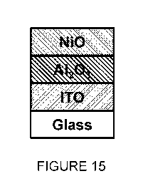
layer of FAPbI3. FIG. 15 illustrates a stylized diagram of an example thin
film stack for sample
numbers 13 to 15, in accordance with certain embodiments. FIG. 16 illustrates
a stylized
diagram of an example film stack for sample numbers 16 to 18, in accordance
with certain
embodiments. In some embodiments, the thin film stack with the NiO layer shown
in FIG. 15
may comprise a substrate, an interfacial layer, and an NiO layer prepared and
deposited by the
methods described herein. In some embodiments, the thin film stack with the
NiO layer shown
in FIG. 16 may comprise a substrate, an interfacial layer, and an NiO layer
prepared and
deposited by the methods described herein, and a layer of perovskite material.
The substrate
may be an ITO-coated glass. The interfacial layer may be an A1203 layer. The
perovskite
material may be FAPbI3.
[00120] The formulation of the NiO precursor ink used to produce the
NiO layer in
sample number in sample numbers 13-17 included 0.72 M nickel nitrate
hexahydrate and 0.1-
110 mM nickel acetate tetrahydrate in a mixed solvent of ethylene glycol,
ethanolamine, and
water having a volume ratio of 12:1.46:1, with additional copper acetate added
to obtain the final
copper and acetate concentrations as described below for each sample. The
formulation of the
NiO precursor ink used to produce the NiO layer in sample number 13 includes 5
mol% Cu and
mol% acetate. The formulation of the NiO precursor ink used to produce the NiO
layer in
sample number 14 includes 0 mol% Cu and 12.5 mol% acetate. The formulation of
the NiO
precursor ink used to produce the NiO layer in sample number 15 includes 5
mol% Cu and 12.5
mol% acetate. The formulation of the NiO precursor ink used to produce the NiO
layer in
sample number 16 includes 5 mol% Cu and 5 mol% acetate. The formulation of the
NiO
precursor ink used to produce the NiO layer in sample number 17 includes 0
mol% Cu and 12.5
mol% acetate. The formulation of the NiO precursor ink used to produce the NiO
layer in
sample number 18 includes 5 mol% Cu and 12.5 mol% acetate. In each of the
above described
samples, the mole percentage of Cu is shown relative to the total combined
moles of Cu and Ni.
The mole percentage of acetate is shown relative to the total combined moles
of acetate and
nickel.
[00121] Some or all of materials in accordance with some embodiments
of the
present disclosure may also advantageously be used in any organic or other
optical, mechanical,
23
CA 03120657 2021-05-20
WO 2020/106542 PCT/US2019/061462
or electronic device, with some examples including, but not limited to:
batteries, field-effect
transistors (FETs), light-emitting diodes (LEDs), non-linear optical devices,
memristors,
capacitors, rectifiers, and/or rectifying antennas.
[00122] Therefore, the present invention is well adapted to attain
the ends and
advantages mentioned as well as those that are inherent therein. The
particular embodiments
disclosed above are illustrative only, as the present invention may be
modified and practiced in
different but equivalent manners apparent to those skilled in the art having
the benefit of the
teachings herein. Furthermore, no limitations are intended to the details of
construction or
design herein shown, other than as described in the claims below. It is
therefore evident that the
particular illustrative embodiments disclosed above may be altered or modified
and all such
variations are considered within the scope and spirit of the present
invention. In particular, every
range of values (of the form, "from about a to about b," or, equivalently,
"from approximately a
to b," or, equivalently, "from approximately a-b") disclosed herein is to be
understood as
referring to the power set (the set of all subsets) of the respective range of
values, and set forth
every range encompassed within the broader range of values. Also, the terms in
the claims have
their plain, ordinary meaning unless otherwise explicitly and clearly defined
by the patentee.
24