Note: Descriptions are shown in the official language in which they were submitted.
CA 03120822 2021-05-21
WO 2020/104807 PCT/GB2019/053297
1
RAPID DUMP OF PARTIALLY INSULATED SUPERCONDUCTING MAGNET
Field of the Invention
The present invention relates to high temperature superconducting, HTS,
magnets. In
particular, the invention relates to a method for ramping down HTS magnets
e.g. in
response to quench detection, and apparatus implementing the method.
Background
Superconducting materials are typically divided into "high temperature
superconductors" (HTS) and "low temperature superconductors" (LTS). LTS
materials,
such as Nb and NbTi, are metals or metal alloys whose superconductivity can be
described by BCS theory. All low temperature superconductors have a critical
temperature (the temperature above which the material cannot be
superconducting
even in zero magnetic field) below about 30K. The behaviour of HTS material is
not
described by BCS theory, and such materials may have critical temperatures
above
about 30K (though it should be noted that it is the physical differences in
composition
and superconducting operation, rather than the critical temperature, which
define HTS
and LTS material). The most commonly used HTS are "cuprate superconductors" -
ceramics based on cuprates (compounds containing a copper oxide group), such
as
BSCCO, or ReBCO (where Re is a rare earth element, commonly Y or Gd). Other
HTS materials include iron pnictides (e.g. FeAs and FeSe) and magnesium
diborate
(Mg B2).
ReBCO is typically manufactured as tapes, with a structure as shown in Figure
1.
Such tape 100 is generally approximately 100 microns thick, and includes a
substrate
101 (typically electropolished hastelloy approximately 50 microns thick), on
which is
deposited by IBAD, magnetron sputtering, or another suitable technique a
series of
buffer layers known as the buffer stack 102,of approximate thickness 0.2
microns. An
epitaxial ReBCO-HTS layer 103 (deposited by MOCVD or another suitable
technique)
overlays the buffer stack, and is typically 1 micron thick. A 1-2 micron
silver layer 104 is
deposited on the HTS layer by sputtering or another suitable technique, and a
copper
stabilizer layer 105 is deposited on the tape by electroplating or another
suitable
technique, which often completely encapsulates the tape.
CA 03120822 2021-05-21
WO 2020/104807 PCT/GB2019/053297
2
The substrate 101 provides a mechanical backbone that can be fed through the
manufacturing line and permit growth of subsequent layers. The buffer stack
102 is
required to provide a biaxially textured crystalline template upon which to
grow the HTS
layer, and prevents chemical diffusion of elements from the substrate to the
HTS which
damage its superconducting properties. The silver layer 104 is required to
provide a
low resistance interface from the ReBCO to the stabiliser layer, and the
stabiliser layer
105 provides an alternative current path in the event that any part of the
ReBCO
ceases superconducting (enters the "normal" state).
In addition, "exfoliated" HTS tape can be manufactured, which lacks a
substrate and
buffer stack, and instead has silver layers on both sides of the HTS layer.
Tape which
has a substrate will be referred to as "substrated" HTS tape.
HTS tapes may be arranged into HTS cables. An HTS cable comprises one or more
HTS tapes, which are connected along their length via conductive material
(normally
copper). The HTS tapes may be stacked (i.e. arranged such that the HTS layers
are
parallel), or they may have some other arrangement of tapes, which may vary
along
the length of the cable. Notable special cases of HTS cables are single HTS
tapes,
and HTS pairs. HTS pairs comprise a pair of HTS tapes, arranged such that the
HTS
layers are parallel. Where substrated tape is used, HTS pairs may be type-0
(with the
HTS layers facing each other), type-1 (with the HTS layer of one tape facing
the
substrate of the other), or type-2 (with the substrates facing each other).
Cables
comprising more than 2 tapes may arrange some or all of the tapes in HTS
pairs.
Stacked HTS tapes may comprise various arrangements of HTS pairs, most
commonly
either a stack of type-1 pairs or a stack of type-0 pairs and (or,
equivalently, type-2
pairs). HTS cables may comprise a mix of substrated and exfoliated tape.
Broadly speaking, there are two types of construction for magnetic coils ¨ by
winding,
or by assembling several sections. Wound coils, as shown in Figure 2, are
manufactured by wrapping an HTS cable 201 around a former 202 in a continuous
spiral. The former is shaped to provide the required inner perimeter of the
coil, and
may be a structural part of the final wound coil, or may be removed after
winding.
Sectional coils, as shown schematically in Figure 3, are composed of several
sections
301, each of which may contain several cables or preformed busbars 311 and
will form
CA 03120822 2021-05-21
WO 2020/104807 PCT/GB2019/053297
3
an arc of the overall coil. The sections are connected by joints 302 to form
the
complete coil. While the turns of the coils in figures 2 and 3 are shown
spaced apart
for clarity, there will generally be material connecting the turns of the coil
¨ e.g. they
may be consolidated by potting with epoxy.
Figure 4 shows a cross section of a specific type of wound coil known as a
"pancake
coil", where HTS cables 401 are wrapped to form a flat coil, in a similar
manner to a
spool of ribbon. Pancake coils may be made with an inner perimeter which is
any 2
dimensional shape. Often, pancake coils are provided as a "double pancake
coil", as
shown in the cross section of Figure 5, which comprises two pancake coils 501,
502
wound in opposite sense, with insulation 503 between the pancake coils, and
with the
inner terminals connected together 504. This means that voltage only needs to
be
supplied to the outer terminals 521, 522, which are generally more accessible,
to drive
current through the turns of the coil and generate a magnetic field.
The coils may be "insulated" ¨ having electrically insulating material between
the turns
of the coil, or "non insulated", where the turns of the coil are electrically
connected
radially, as well as along the cables (e.g. by connecting the copper
stabiliser layers of
the cables by soldering or by direct contact). "Partially insulated" coils are
also
possible, where the turn to turn resistance is less than that of a traditional
insulator,
such as ceramic or organic insulator, but greater than the resistance between
tapes in
a cable of the coil ¨ e.g. between 100 and 1015 times the resistance between
tapes in a
cable. Having no or partial insulation between turns slows the rate at which
the
temperature of a local "hotspot" (normal zone) rises because it allows current
to share
between turns.
A non-insulated HTS coil can be modelled as having three current paths ¨ two
spiral
paths, which follow the HTS tapes (one in the HTS and one in the metal
stabilizer), and
a radial path through the metal (and any other resistive material) connecting
the non- or
partially- insulated HTS cable turns between the coil terminals (while this
can be
modelled as a single path, it in fact represents the sum of all radial
resistive paths
through the magnet). Only current flowing in the spiral paths generates
significant axial
magnetic field in the centre of the coil. The HTS spiral path can be modelled
as an
inductor having a large inductance and zero or negligible resistance when the
tape is
all superconducting. The copper stabilizer spiral path is in parallel with the
HTS path
CA 03120822 2021-05-21
WO 2020/104807 PCT/GB2019/053297
4
and has the same inductance, but significant resistance. For this reason
negligible
current flows in it unless parts of the HIS spiral path start to quench. If
this happens
the excess current above the critical current lc of the HIS spiral path shares
between
the spiral stabilizer path and the radial path according to their relative
resistances and
L/R time constants. The radial current path can be modelled as having a
negligible
inductance and a much greater resistance than the spiral path while the HIS is
superconducting throughout.
One potential use of HIS field coils is in tokamak plasma chambers,
particularly for
nuclear fusion reactors. WO 2013/030554 describes an approach involving the
use of
a compact spherical tokamak for use as a neutron source or energy source. The
low
aspect ratio plasma shape in a spherical tokamak improves the particle
confinement
time and allows net power generation in a much smaller machine. However, a
small
diameter central column is a necessity, which presents challenges for design
of the
plasma confinement magnet. High temperature superconductor (HIS) field coils
are a
promising technology for such magnets.
Another potential use of HIS field coils is in proton beam therapy devices.
Proton
beam therapy (PBT, also known as proton therapy) is a type of particle therapy
used in
the treatment of cancers (and other conditions which respond to radiotherapy).
In PBT,
a beam of protons is directed towards the treatment location (e.g. the
tumour).
Another, similar therapy is proton boron capture therapy (PBCT), in which
boron-11 is
introduced to the target location, and a proton beam is used to initiate the
+p 1 1 B _, 3a
reaction. The same apparatus can be used to provide proton beams for either
PBT or
PBCT.
The proton beams for PBT and PBCT are generated by particle accelerators such
as a
cyclotrons or linear accelerators. Accelerators typically used for PBT and
PBCT
typically produce protons with energies in the range of 60 to 250MeV, with the
most
powerful currently operating facility having a maximum energy of 400 MeV.
There are, broadly speaking, two types of design for PBT devices which allow
variation
of the beam angle. In the first type of design, as illustrated in Figure 6,
the accelerator
3001 is mounted on a gantry 3002, which allows it to be rotated around the
patient
3003 (usually about a horizontal axis). The patient is placed on a moveable
bed 3004,
CA 03120822 2021-05-21
WO 2020/104807 PCT/GB2019/053297
which provides further degrees of freedom (e.g. translational motion and
rotation about
a vertical axis).
The second type of design is illustrated in Figure 7. The accelerator 4001 is
stationary,
5 and the beam is directed to the patient via steering magnets 4002
(generally including
both quadrupole and dipole magnets), at least some of which are located on a
gantry
4003, such that the beam can be rotated around the patient 4004 (e.g. about a
horizontal axis). The patient is placed on a moveable bed 4005.
Either design requires that the gantry hold electromagnets capable of steering
protons
at the beam energy, which could be as high as 400MeV. This requires very high
magnetic fields, and as such the use of HTS field coils can considerably
reduce the
mass and size of the electromagnets and the gantry needed to move them. HTS
field
coils may be used within the accelerator, quadrupole magnets of the steering
magnets,
or dipole magnets of the steering magnets.
Summary
The invention is defined in the appended claims.
Brief Description of the Drawings
Figure 1 is a schematic representation of an HTS tape;
Figure 2 is a schematic representation of a wound HTS coil;
Figure 3 is a schematic representation of a sectional HTS coil;
Figure 4 is a cross section of a pancake coil;
Figure 5 is a cross section of a double pancake coil;
Figure 6 is a schematic representation of a first PBT device;
Figure 7 is a schematic representation of a second PBT device;
Figure 8 shows results of a simulation of a partially insulated coil;
Figure 9 shows results of a simulation of an exemplary magnet system
Figure 10 shows graphs of magnetic field and temperature for a coil following
simply
shutting off the power supply;
Figure 11 shows the voltages for a coil during the same process as shown in
Figure 10;
Figure 12 A and B show an example of leaky insulation;
CA 03120822 2021-05-21
WO 2020/104807 PCT/GB2019/053297
6
Figure 13 A and B show a further example of leaky insulation;
Figure 14 shows an equivalent circuit to a two turn coil.
Detailed Description
Figure 8 shows the current, voltage, and power in a non-insulated coil during
ramp-up
and into steady state operation. During ramp-up of a non-insulated coil,
current will
initially flow primarily in the radial path (period A in Fig 8), and then
stabilize. The
amount of current flowing in the radial path is higher for faster ramp rates
(since the
voltage developed across the spiral path, L.dl/dt, is higher ¨ this is period
B). At the
end of the ramp, dl/dt drops to zero and current will transfer to the HTS
spiral path with
a time constant L/R (period C). The current will be mostly transferred into
the spiral
path a few (approximately five) L/R time constants after the end of the ramp.
As such,
the time constant should be selected to result in a reasonable ramp-up time,
e.g. a time
constant of 5-10 hours would be acceptable for the TF coil of a tokamak
(giving a
ramp-up time of about 1-2 days).
In a large magnet, in order to avoid damage from a quench (in either an
insulated or
non-insulated coil), an active quench protection scheme may also be
implemented. In
this scheme the magnet's stored energy may be dumped into some component other
than the quenching region of the magnet before sufficient temperature rise can
occur in
the quenching region to cause damage. The other component may be an external
resistance, or a separate portion of the magnet which is quenched over a
larger
proportion of the magnet's cold mass (thereby distributing the magnet's stored
energy
over a large volume, and reducing the overall temperature rise). However, the
active
approach requires the time between initiation of the normal zone (also called
a "hot
spot") and triggering of the magnet current ramp-down ("dump") to be short
enough
that the terminal temperature of the hot spot is less than a temperature at
which
damage to the coil can occur, eg: around 200 K. Such an approach may also be
used
in small magnets, to provide further protection against quenches.
The above, as well as discussion of suitable constructions to achieve a
desired time
constant, is discussed in more detail in co-pending application GB1818817.7
Although the use of PI coils extends the time available to dump the magnet
current, it is
still important that this operation is done as quickly as possible following
detection of a
CA 03120822 2021-05-21
WO 2020/104807 PCT/GB2019/053297
7
hot spot. There has been relatively little discussion of current dumping
techniques for
PI coils, as in the literature PI coils are generally only used for smaller
coils ¨ in which
the total energy of the coil is relatively low, and the quench will tend to
propagate
through the entire coil relatively quickly ¨ meaning that the energy dump is
spread
through the coil. In addition, PI coils are inherently stable when compared to
insulated
coils, and so can often operate without quench protection as the risk is low.
However,
in large coils with considerable stored energy, coils with geometry that
allows the hot
spot to cover all the turns over only a relatively small proportion of the
coil winding,
and/or coils intended for long term operation in hostile environments (e.g.
field coils for
a nuclear fusion reactor), active quench protection is important.
The use of PI coils provides further advantages when dumping energy from the
magnet. Figure 10 shows graphs of magnetic field (proportional to spiral path
current)
and temperature for a coil following simply shutting off the power supply
(i.e. making it
an open circuit). During period A, the power supply is turned on (shown by the
current
1001). At the start of period B, the power supply is shut off, causing the
coil's
inductance to generates a voltage which continues to drive the current in each
turn in a
closed loop, shorting back to the start of the turn via the turn-turn
resistance. This
causes ohmic heating which reduces the critical current in the HTS. This
process
continues for through period B (typically a few seconds, depending on many
factors, 14
seconds in this experiment) until the HTS in the turn quenches and generates
sufficient
voltage to eject its loop current into the metal stabilizer in the spiral path
(period C).
Since this has a much higher resistance than the turn-turn resistance the
turn's
magnetic field energy is rapidly converted to heat in the stabilizer and the
turn
temperature rises uniformly as the spiral path current quickly drops to 0
(<1s).
However, for effective quench protection, a longer period B is still
undesirable ¨ in the
event of a quench, this period may be long enough for significant local
heating to occur
in a local hot spot elsewhere in the magnet, resulting in an unacceptably high
peak
temperature in that hot spot. Furthermore, a magnet, such as a TF magnet in a
tokamak, may comprise several coils (eg: separate limbs) that are poorly
thermally and
magnetically coupled, It is desirable that, when triggering a dump by turning
off the
power supply, all of the coils experience the same delay before quenching.
Variations
between coils may occur due to manufacturing differences of local temperature
of
magnetic field differences. If the coils quench non-simultaneously the
resultant very
CA 03120822 2021-05-21
WO 2020/104807 PCT/GB2019/053297
8
large electromagnetic forces between coils may cause damage to the magnet's
mechanical support structure, and/or the coils themselves. To minimise this it
is
desirable to minimise the variation between the delay between PSU off and
quench in
each coil, so that any variation between delays durations is also minimised.
The length
of this period could be reduced by increasing the resistance of the partially
insulating
layer (and thereby increasing the heating due to current travelling in the
radial path in
period B), but this would have knock-on effects to other electrical properties
of the coil,
e.g. altering the time constant for ramping up the coil, or making current
sharing
between turns more difficult (which will increase the likelihood of a hot-spot
causing a
global quench).
Instead, rather than shutting off the power supply, it is proposed to apply a
large
reverse current to the magnet coil (i.e. in the opposite direction to the
current flowing
through the coil prior to the ramp-down), e.g. by using a four-quadrant PSU
which is
able to sink current from the magnet coil. The superconducting path has a
large
inductance, and so this reverse current will flow primarily in the radial path
in all the
coils of the TF magnet. This large increase in radial current causes
significant heating
of all coils, rapidly quenching the entire magnet (and therefore spreading the
energy
dump over a large area).
While it may seem counterintuitive to apply a reverse current rather than
simply
shutting down the PSU, the important distinction is that the excess radial
current will
heat the whole bulk of the magnet ¨ which means that the quench will quickly
spread
through the magnet and the energy dump will be spread through the whole volume
(or
at least a significant fraction). A concentrated energy dump, as would occur
without
any intervention, would cause unacceptable temperature rises in that small
area,
damaging the HTS. If a significant portion of the magnet is quenched, the same
amount of energy (plus a small contribution from the reverse current itself)
is spread
throughout the magnet, which limits the temperature rise in the HTS. In
addition,
heating the magnet more evenly prevents steep temperature gradients from
forming
within the magnet. If the temperature gradient is too high, then the differing
thermal
expansion of nearby regions of the magnet will cause structural damage.
In existing magnets, even heating would be achieved by the use of "quench
heaters" ¨
i.e. heating elements laid adjacent to the HTS cable, which can be turned on
to deliver
CA 03120822 2021-05-21
WO 2020/104807 PCT/GB2019/053297
9
heat to the coil. However, such heaters take up space, and as such reduce the
available space for HIS conductor or for metal stabiliser. The "reverse
current"
method in effect uses the radial conduction path as a "quench heater", meaning
that
the heating is evenly distributed through the coil, and additional heating
elements are
not required.
The reverse current may be limited to, or set at, the operating current of the
magnet. In
this way, the maximum heating is achieved by the reverse current without
exceeding
the design parameters of components external to the magnet, compared to what
would
be required for normal magnet operation.
The above has been described with reference to quench protection, but it
should be
noted that the energy dumping technique described above may also be applicable
to
other situations where the magnet is ramped down ¨ e.g. when shutting the
magnet
down under ordinary conditions, in the absence of any detected quench (or
conditions
likely to lead to a quench).
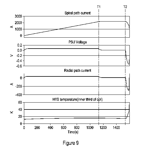
Figure 9 shows simulation results of an exemplary partially insulated coil
during ramp-
up, steady state operation, and ramp-down. In this case, the PSU (power
supply) is
modelled as a current source, i.e. the current supplied by the PSU is set in
the
simulation, and the voltage across the PSU is calculated.
During ramp-up the PSU current increases steadily to 2.2[<A at a constant
rate. The
PSU voltage is positive, and on the order of 0.1V. The current in the radial
path is
approximately proportional to the PSU voltage (as the radial path can be
modelled as a
simple resistance), and the current in the spiral path increases at a constant
rate. At
time Ti, when the desired current is reached, the magnet is switched to steady
state
operation ¨ the PSU is set to a constant current, and the radial path current
decreases
with time constant URradial as described previously. The PSU voltage decreases
to a
value on the order of a few millivolts when the radial path current has
decayed, as the
spiral path has negligible resistance (in this simulation, it is modelled as
having zero
resistance ¨ so the PSU voltage tends to zero. In practice, it will generally
settle
around a few 10s-100s of millivolts). During ramp-up and steady state
operation, the
HTS temperature is substantially constant below 20K.
CA 03120822 2021-05-21
WO 2020/104807 PCT/GB2019/053297
At time 12, a magnet dump is initiated (either in response to a quench
detection or
otherwise). The PSU supplies a reverse current (with a fast current ramp,
modelled in
this case as a downwards current ramp ten times faster than the initial ramp-
up), which
flows primarily in the radial path. The PSU voltage is negative during the
supply of this
5 current, on the order of -0.5V. The HTS temperature rises quickly. The
simulation
ends when the HTS temperature reached approx 55K, as the entire coil will
quench,
and the temperature rise becomes too fast for the model used. However, in
reality the
magnet's stored energy would be rapidly converted to heat, spread relatively
uniformly
over the magnet, safely shutting it down.
The reverse current may be supplied for a set time, or until a specified
condition is
reached ¨ e.g. on detection of a quench in a substantial portion of the
magnet,
detection of a specified temperature in a substantial portion of the magnet,
or detection
that the spiral path current (or the magnetic field generated by the coil) has
decreased
below a threshold value.
The speed of the ramp-down is dependent on the speed of the reverse current
ramp in
the PSU.
It is desirable to be able to control the rate of change of current during
both the magnet
ramping phase and the dump phase. For this reason, a PSU with feedback
controlled
current output is preferred. The PSU current may be controlled on the basis of
the
current in the spiral path, the temperature of the magnet, the magnetic field
generated
by the coil, or any other suitable property of the coil.
The power supply may comprise multiple power supply units, each of which
provides
power to the coil during a different period. In particular, the power supply
may
comprise a first unit for supplying power to the coil during ramp-up and
steady state
operation, and a second unit for supplying the reverse voltage to the coil
during ramp-
down.
The power supply (or one or more power supply units of the power supply) may
be
partially located within the cryostat containing the HTS magnet, and may
comprise a
transformer arranged to transfer power across the cryostat without having
cables
passing through the cryostat, as described in PCT/GB2018/050337.
CA 03120822 2021-05-21
WO 2020/104807 PCT/GB2019/053297
11
Where ramp-down of the magnet is triggered in response to detection of a
quench or
conditions likely to lead to a quench, this detection may be by any practical
method.
For example:
= detection of an excess voltage across the HIS material in the magnet;
= the use of secondary HIS tapes which are provided adjacent to the main
coil,
and configured to quench before the main coil, e.g. as described in
international
patent application PCT/GB2016/052712 or UK patent application GB1812120.2
= detection of temperature, strain, magnetic fields, or other conditions
within the
magnet coil, e.g via Raleigh scattering in fibre optic cables as described in
international patent application PCT/GB2017/053066 or via other temperature,
strain, or magnetic field detectors as known in the art.
It is important not to apply reverse current for too long, otherwise the
active dump could
warm the magnet above 200K and cause problems. Ideally the dump system should
limit the total energy applied to the magnet to that required to raise the
temperature of
the whole magnet above it's critical temperature (ie: turn all coils from
superconducting
to normal). This is a small fraction of the total energy needed to raise the
whole magnet
to -200K. As the coils begin to quench, the magnet's own stored energy will be
dissipated, driving the global quench.
A simple way to apply the correct amount of energy is to discharge a capacitor
bank
into the magnet. This also avoids the need for a four-quadrant PSU. A single
quadrant
PSU may be used to ramp the magnet. When it is necessary to dump the magnet
this
is simply disconnected using active switches and a pre-charged capacitor bank
connected across the magnet to drive the reverse radial current. Note that no
large
voltages are generated by disconnecting the PSU since the large inductance of
the
magnet is shunted by its radial resistance
Most of the above disclosure has been focussed on ramping down a magnet
following
quench detection, where the speed of the ramp-down is of critical importance.
There
are also techniques using the same underlying principle which are applicable
to
controlling the magnet in conditions where the ramp-down time is not the
primary
factor..
CA 03120822 2021-05-21
WO 2020/104807 PCT/GB2019/053297
12
As an example, the PSU may be configured to supply a ramp-down current which
is
less than the current in the magnet, but in the same direction. This will
cause a current
equal to the difference between the magnet and PSU currents to run in the
radial path,
heating the magnet as before. This will result in a slower ramp down compared
to a
reverse current (or simply disconnecting the PSU), and a reduced temperature
rise in
the magnet.
As a further example, the PSU may be configured to supply an AC current
overlaid on
the DC delivered to the coil (either during steady state, ramp-up, or ramp-
down).
Where the period of the AC current is significantly less than the time
constant L/R, this
AC current will flow entirely in the radial path. This results in heating of
the magnet
without otherwise affecting the current in the spiral path (compared to the
case where
only the DC current is delivered).
The overlaid AC current may also be used in combination with any of the
previous
examples. For example, a combination of a DC reverse current and an AC current
(i.e.
where the total current is a sinusoidal current with an average value which is
opposite
in sign to the coil current, and a period less than the time constant of the
magnet) may
be used to ramp down the coil with additional heating. Alternatively, the AC
current
may be combined with a DC ramp down current which is less than the current in
the
magnet, but in the same direction (i.e. where the total current is a
sinusoidal current
with an average value which is less than the coil current, and a period less
than the
time constant of the magnet). As a further alternative, a purely AC current
may be
provided to ramp down the magnet ¨ this will cause a current equal to the
magnet
current to run in the radial path, in addition to the AC current. In each
case, adding the
AC current results in a greater current in the spiral path (and hence quicker
ramp
down) compared to using only the DC current.
A surprising feature of ramping down a partially insulated coil as discussed
in the
above examples (either by shutting down the PSU or by providing a modified
current) is
that the turn to turn voltage of the coil remains low (on the order of a few
volts, even for
large coils) throughout the process. Large insulated superconducting coils
require
heavy duty insulation, which can withstand very high voltages ¨ but the small
voltages
experienced by a partially insulating coil could be insulated against
effectively by a
much wider variety of materials (or even a simple vacuum or air gap).
CA 03120822 2021-05-21
WO 2020/104807 PCT/GB2019/053297
13
Figure 11 shows the voltage across each coil in the same magnet as used in
Figure 10
(which contains 6 pancake coils, with a total inductance of 0,12H). The peak
voltages,
which occur at a time corresponding to the start of the global quench (i.e.
the end of
period B and beginning of period C in figure 10) are about 0.1V. In contrast,
the
expected voltage for an equivalent insulated coil under the same conditions
would be
on the order of at 2kV, and the expected voltage for a large coil would be at
least 5kV
(the voltage can be calculated as V=-L dl/dt, where dl/dt is approximately the
transport
current (1.4kA for the test coil) divided by the time taken to quench (0.1kA
for the test
coil)). In a partially insulated coil, the coil can be operated at high
transport current and
inductance without a particularly high voltage developing ¨ which is most
practical
when operating a large coil at low transport currents (a few kiloamps,
compared to
typically 50kA) and high inductance (i.e. a higher number of turns).
The peak voltage generated between two turns of a partially insulating coil
during
current dump with an open circuit PSU can be approximated as V=IoRstab, where
lo is
the transport current, and Rstab is the resistance of the resistive material
in the spiral
path of the coil.. The quench propagates between coils by mutual inductance,
which
means that the peak coil voltage does not exceed the peak voltage for a single
turn.
The peak voltage will not exceed 10V for any realistically large coil.
Figure 14 shows the equivalent circuit for a coil with 2 turns (and can be
extended to
more turns by adding more coils in series, and mutual inductances between each
coil).
In this figure, lo is the transport current, Rtt is the turn to turn
resistance (i.e. the radial
path resistance divided by the number of turns), Rstab is the resistance of
the resistive
spiral path, Lturn is the induction of each turn, and RHTs is the resistance
of the HTS in
each turn (i.e. 0 during normal operation, and only non-zero during a quench
or near-
quench). M is the mutual induction between the two turns, and K is the
coupling
coefficient between the turns.
This is of particular importance for insulation of the coil ¨ both for
insulation of the coil
as a whole from other components ("ground wrap"), and for designs of partial
insulation
which use insulating material having a number of conductive channels through
it
(known as "leaky insulation", and discussed in more detail below). The low
voltage
means that the insulation does not need to be a heavy duty material such as
Kapton TM
CA 03120822 2021-05-21
WO 2020/104807 PCT/GB2019/053297
14
(as used in conventional insulated magnets), but simpler materials such as
paint,
varnish, or even paper can be used, or the insulating material can be replaced
by an air
or vacuum gap (with suitable support structures, also insulators if required).
Insulating structures can be characterised by a "breakdown voltage", above
which the
structure ceases insulating and the resistance of the structure drops from the
order of
several megaOhms to the order of a few Ohms or milliOhms. For an insulated
coil, this
breakdown voltage would need to be at least 2kV (at least 5kV for large coils,
e.g. with
a radius greater than 50cm), which severely limits the materials that can be
used while
still keeping the insulation reasonably compact (the breakdown voltage is
approximately proportional to the thickness of the material, with the
proportionality
constant ("dielectric constant") depending on the material).
For a partially insulating coil, only a breakdown voltage greater than 10V or
so is
required ¨ which would allow the use of any material that can be reasonably
called an
"insulator"
Alternatively, in environments hostile to materials (e.g. in a fusion reactor,
where the
materials will be subject to neutron bombardment), this allows for insulation
to be used
for longer before degrading to the point where it is no longer insulating ¨ as
neutron
bombardment will tend to cause changes in insulation which will reduce its
dielectric
constant, or introduce physical gaps.
An example of leaky insulation is shown in Figure 12A and B. The metal strip
901 is
provided with a thin insulating coating 902 on at least the sides facing the
HTS cables,
where the insulating coating is removed or missing over windows (or "through
holes")
903 at intervals on each side of the metal strip. The windows can have any
shape and
can extend to the edges of the tape. The location of windows on either side of
the
metal strip are staggered, as shown in Figure 12B, which increases the
resistance
(compared to an uninsulated strip, or to a strip where the windows on each
side were
directly opposite each other) as the current must take a path 910 along part
of the
length of the metal strip.
By varying the spacing of the windows such that they are closer together in
the return
limbs and further apart in the core, the required difference in turn to turn
resistance
CA 03120822 2021-05-21
WO 2020/104807 PCT/GB2019/053297
between the return limbs and core can be achieved. Further tuning may be
achieved
by using a different metal for the metal strip in the core compared to in the
return limbs,
or by varying other aspects of the geometry of the strip.
5 To allow for even further tuning, rather than a solid metal strip, a
layer having several
metal tracks may be used ¨ effectively forming an insulating layer having
conductive
radial tracks disposed within it, where the spacing and length of the tracks
determines
the resistance of the partially insulating layer.
10 Figures 13 A to E show a further example leaky insulation layer. The
leaky insulation
layer comprises 5 layers, which are, in order:
= a first metal connection layer 1611;
= a first insulating layer 1621;
= an electrically conducting layer 1630;
15 = a second insulating layer 1622;
= a second metal connection layer 1612.
Figures 13 A to C show the layout of the first metal connection layer 1611,
electrically
conducting layer 1630, and second metal connection layer 1622 respectively.
Figures
13 D and E are cross sections along the lines D and E in Figures 13 A to C.
The connection layer is present to facilitate attachment to HTS cables by
soldering.
In contrast to the previous example where the electrically conducting layer is
a
continuous metal strip, in this example the electrically conducting layer is
divided into
several conductive regions. These regions come in two types. The square
regions
1631 (though they may be any shape in practice) are connected by vias 1606
only to
one of the metal connection layers. These regions do not affect the electrical
properties of the partially insulating layer, but provide a thermal path
through the
respective insulating layer. By varying the size of these regions and the
number of
connections between them and the metal connection layer, the thermal
properties of
the partially insulating layer can be varied independently of the electrical
properties.
The other regions 1632 each connect a window 1601 of the first insulating
layer 1621
to a window 1602 of the second insulating layer 1622. The resistance between
the
CA 03120822 2021-05-21
WO 2020/104807 PCT/GB2019/053297
16
windows can be controlled by varying the geometry of the regions 1632 ¨ e.g.
where
the region 1632 contains a track 1633 which is elongate as shown in Figure
13B,
increasing the width of the track would reduce the resistance between the
windows,
and increasing the length of the track (e.g. by providing a non-linear track,
or by moving
the windows) would increase the resistance between windows.
The windows 1601 in the first insulating layer are formed by drilled vias
through the first
connection layer and the first insulating layer, which are then plated with
metal 1603 (or
other electrically conductive material) to connect the first connection layer
and the
electrically conductive layer. The windows 1602 in the second insulating layer
are
formed by drilling a via 1602 through all of the layers, which is then plated
with metal
1604 (or other electrically conductive material). To prevent a connection
being formed
to the first connection layer through the windows 1602 of the second
insulating layer,
the first connection layer is etched around the via 1602 to electrically
isolate it, and an
insulating cap 1605 is placed on the end of the via 1602 to ensure no bridging
occurs
due to soldering or contact with the HTS cable.
As an alternative, the windows 1602 may instead be drilled from the other side
of the
partially insulating layer, such that they pass through the second connection
layer,
second insulating layer, and electrically conducting layer, and do not pass
through (or
do not pass completely through) the first insulating layer. As a further
alternative, all
the windows may be formed from vias which pass through all layers, with
etching of the
second connection layer and an insulating cap on the second connection layer
being
used for windows 1601 of the first insulating layer.
Another unexpected advantage of partially insulated coils is that the
additional quench
stability allows a greater choice of materials for the non-superconducting
conductive
elements within each cable. In conventional coils, both the stabiliser of the
HTS (i.e.
the thin layer of metal or metal cladding on each tape) and any material
connecting the
tapes would be copper ¨ as it has a very low resistivity, and higher
resistivity materials
would cause excessive heating. However, copper is also a relatively soft
metal, so
under high pressures it can be squeezed out of the tape, or can deform under
shear
stresses which is likely to be responsible for the damage to the HTS layers
following a
quench.
CA 03120822 2021-05-21
WO 2020/104807 PCT/GB2019/053297
17
Therefore, it is preferable to reduce or eliminate copper from the turns of
the coil and
the partial insulation. Reduced copper may be, for example, less than 10
microns
thickness of copper per HTS tape in the coil (i.e. reduced compared to
conventional
HTS tapes), or less than 5 microns thickness of copper (i.e. less than half
that). The
metals or other electrical conductors used in place of copper may have one or
more of:
= reduced ductility compared to copper;
= an increased shear modulus compared to copper;
= an increased Young's modulus compared to copper;
= an increased bulk modulus compared to copper;
= an increased Brinell Hardness Number compared to copper.
Suitable materials include stainless steel.
The above disclosure can be applied to a variety of HTS magnet systems. In
addition
to the tokamak fusion reactor mentioned above as an example, it may be used
for HTS
coils in nuclear magnetic resonance imaging (NMR / MRI) devices, manipulation
of
magnetic devices within a non-magnetic medium via magnetic fields (e.g.
robotic
magnetic navigation systems for manipulating medical devices within a
patient), and
magnets for electric motors, e.g. for electronic aircraft. As a further
example, the
disclosure may be applied to proton beam therapy devices comprising HTS magnet
systems which include the disclosed features, where the HTS magnet systems are
used within the accelerator of the PBT device, the quadrupole or dipole
steering
magnets of the PBT device, or any other magnet of the PBT device.