Note: Descriptions are shown in the official language in which they were submitted.
1
MULTI-LOCATION LOAD CONTROL SYSTEM
100011
BACKGROUND
[0002] Three-way and four-way switch systems may be used for controlling
electrical loads,
such as lighting loads. Typically, the switches are coupled together in series
electrical connection
between an alternating-current (AC) power source and the lighting load. The
switches are subjected
to an AC source voltage and carry full load current between the AC power
source and the lighting
load, as opposed to low-voltage switch systems that operate at low voltage and
low current, and
communicate digital commands (usually low-voltage logic levels) to a remote
controller that
controls the level of AC power delivered to the load in response to the
commands. Thus, as used
herein, the terms "three-way switch", "three-way system", "four-way switch",
and "four-way
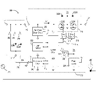
system" mean such switches and systems that are subjected to the AC source
voltage and caffy the
full load current.
[0003] A three-way switch derives its name from the fact that it has three
terminals and is
more commonly known as a single-pole double-throw (SPDT) switch, but will be
referred to herein
as a "three-way switch". Note that in some countries a three-way switch as
described above is
known as a "two-way switch". A four-way switch is a double-pole double-throw
(DPDT) switch
that is wired internally for polarity-reversal applications. A four-way switch
is commonly called an
intermediate switch, but will be referred to herein as a "four-way switch". In
a typical, prior art
Date Recue/Date Received 2022-11-07
2
three-way switch system, two three-way switches control a single lighting
load, and each switch is
fully operable to independently control the load, irrespective of the status
of the other switch. In
such a three-way switch system, one three-way switch must be wired at the AC
power source side of
the system (sometimes called "line side"), and the other three-way switch must
be wired at the
lighting load side (sometimes called "load side") of the system.
100041 Three-way dimmer switches that replace three-way switches are known
in the art.
The three-way dimmer switch may include a dimming circuit (e.g., a phase-
control dimming circuit)
and a three-way switch. The dimmer circuit may regulate the amount of energy
supplied to a
lighting load by conducting for some portion of each half cycle of the AC
source voltage, and not
conducting for the remainder of the half cycle. Because the dimming circuit is
in series with the
lighting load, the longer the dimming circuit conducts, the more energy will
be delivered to the
lighting load. Where the lighting load is a lamp, the more energy that is
delivered to the lighting
load, the greater the light intensity level of the lamp. In a typical dimming
operation, a user may
adjust a control to set the light intensity level of the lamp to a desired
light intensity level. The
portion of each half cycle for which the dimming circuit conducts is based on
the selected light
intensity level. The user is able to dim and toggle the lighting load from the
three-way dimmer
switch and is only able to toggle the lighting load from the three-way switch.
Two three-way
dimmer switches cannot control a common lighting load since two dimming
circuits cannot be wired
in series.
100051 Multiple location dimming systems employing a smart dimmer and one
or more
specially-designed remote (or "accessory") dimmers have been developed. A
smart dimmer may be
one that includes a dimming circuit and a microcontroller or other processing
means for providing an
advanced set of control features and feedback options to the end user. For
example, the advanced
features of a smart dimmer may include a protected or locked lighting preset,
fading, and double-tap
to full intensity. The microcontroller controls the operation of a
semiconductor switch of the
dimming circuit to thus control the intensity of the lighting load. To power
the microcontroller, the
smart dimmer may include one or more power supplies, which draw a small amount
of current
through the lighting load when the semiconductor switch is non-conductive each
half cycle. The
power supply typically uses this small amount of current to charge a storage
capacitor and develop a
direct-current (DC) voltage to power the microcontroller.
Date Recue/Date Received 2022-11-07
3
[0006] An accessory dimmer may not include a dimming circuit, but may be
used to adjust
the intensity level of the lighting load from multiple locations by sending
signals to a smart dimmer
indicating a user input received (e.g., actuation of an actuator) on the
accessory dimmer. The signal
is usually sent through an accessory-dimmer line connecting the accessory
dimmer and the smart
dimmer. In response to such signals, the smart dimmer can exercise control
over the lighting load
using one or more advanced features of the smart dimmer. The accessory dimming
may not include
a microcontroller or other processing means for providing an advanced set of
control features and
feedback options to the end user. An example of a multiple location lighting
control system,
including a wall-mountable smart dimmer switch and wall-mountable remote
switches for wiring at
all locations of a multiple location dimming system, is disclosed in commonly
assigned U.S. Patent
No. 5,248,919, issued on September 28, 1993, entitled LIGHTING CONTROL DEVICE.
[0007] The multiple location lighting control system described above may
suffer from one or
more drawbacks. For example, the signal generated by the accessory dimmer
indicating a user input
may be subject to the impact of line and/or load conditions (e.g., long run of
wires, capacitive
holdup, etc.) of the multiple location lighting control system. Such line
and/or load conditions may
cause the smart dimmer to miss or misinterpret the signals sent by the
accessory dimmer, and
thereby fail to control the lighting load according to the user input received
at the accessory dimmer.
SUMMARY
[0008] Described herein is a multi-location load control system comprising
a load control
device (e.g., a main load control device) and at least one accessory control
device. The load control
device may be configured to control an amount of power delivered to an
electrical load from an AC
power source. The load control device may comprise a first main terminal, a
second main terminal,
and an accessory terminal. The load control device may conduct a load current
from the AC power
source to the electrical load via the first and second main terminals. The
load control device may be
coupled to the accessory control device and receive an input signal from the
accessory control device
indicating an actuation state of the accessory control device. Such actuation
state may correspond
to, for example, toggling the electrical load on and off, raising the amount
of power delivered to the
electrical load, or lowering the amount of power delivered to the electrical
load.
Date Recue/Date Received 2022-11-07
4
[0009] The load control device may further comprise a multi-location
circuit configured to
sense the input signal and generate a multi-location signal in response to the
input signal. A control
circuit of the load control device may control the amount of power delivered
to the electrical load
based on the multi-location signal. More specifically, the control circuit may
sample (e.g., via an
analog-to-digital converter (ADC)) the multi-location signal and determine a
pattern of the multi-
location signal over one or more half cycles of an AC mains line voltage
generated by the AC power
source. The control circuit may determine the pattern based on a high
threshold and a low threshold,
and may dynamically adjust the high threshold based on an indication of a
voltage across the main
load control device. In addition, the load control device may include
additional circuitry configured
to further discharge voltages developed in the multi-location system under
long wire run and/or other
abnormal load conditions. The control circuit may determine the actuation
state of the accessory
control device in response to the detected pattern and may generate a control
signal to control the
amount of power delivered to an electrical load in accordance with the
actuation state of the
accessory control device.
BRIEF DESCRIPTION OF THE DRAWINGS
[0010] FIG. 1 is a block diagram of an example of a multiple-location
load control system,
e.g., a multiple location dimming system.
[0011] FIG. 2 is a simplified block diagram of an example load control
system including a
main dimmer and an accessory dimmer.
[0012] FIG. 3 is a simplified partial schematic diagram of another
example load control
device showing a multi-location circuit in greater detail.
[0013] FIG. 4A shows simplified waveforms that illustrate the operation
of a multi-location
circuit the load control device of FIG. 3 when the load control device is
using a forward
phase-control dimming technique.
[0014] FIG. 4B shows simplified waveforms that illustrate the operation
of a multi-location
circuit the load control device of FIG. 3 when the load control device is
using a reverse
phase-control dimming technique.
Date Recue/Date Received 2022-11-07
5
[0015] FIG. 5 is a simplified partial schematic diagram of another example
load control
device showing a multi-location circuit in greater detail.
[0016] FIGs. 6 and 7 show simplified flowcharts of example control
procedures that may be
executed by a control circuit of a load control device.
[0017] FIG. 8 is a simplified flowchart of an example multi-location
processing
procedure that may be executed by a control circuit of a load control device.
DETAILED DESCRIPTION
[0018] FIG. 1 is a block diagram of an example of a multiple-location load
control
system 100, e.g., a multiple location dimming system. The multiple-location
load control
system 100 may comprise a main load control device, e.g., a main dimmer 102,
and one or more
remote load control devices, e.g., two accessory dimmers 104. The main dimmer
102 and accessory
dimmers 104 may be coupled in series electrical connection between an
alternating-current (AC)
power source 106 and a lighting load 108, for example, via a traveler wiring
111. The traveler
wiring 111 may couple the AC power source 106 to the lighting load 108 via the
main dimmer 102
and one or more accessory dimmers 104, for example, to provide power to the
lighting load 108.
Neutral wiring 112 may couple the lighting load 108 back to the AC power
source 106, for example,
to provide a return path for any remaining power provided by the AC power
source 106 and not
dissipated by the lighting load 108. The accessory dimmers 104 may be wired to
the line side of the
load control system 100 (e.g., to the left of the main dimmer 102 as shown in
FIG. 1 and/or at the
AC power source side of the system) or the load side of the load control
system 100 (e.g., to the right
of the main dimmer 102 as shown in FIG. 1 and/or at the lighting load side of
the system). Further,
the load control system 100 may include any number of (e.g., more or less than
two) accessory
dimmers 104.
[0019] The main dimmer 102 may comprise a first main terminal and a second
main
terminal. For example, the main dimmer 102 may comprise a hot terminal H
(e.g., a line-side
terminal) adapted to be coupled to the line side of the load control system
100 and a dimmed-hot
terminal DH (e.g., a load-side terminal) adapted to be coupled to the load
side of the load control
system 100. The main dimmer 102 may comprise a load control circuit coupled
between the hot and
Date Recue/Date Received 2022-11-07
6
dimmed-hot terminals for controlling the amount of power delivered to the
lighting load 108 (e.g.,
the main dimmer may be configured to conduct a load current from the AC power
source to the
electrical load via the hot and dimmed-hot terminals). The main dimmer 202 may
comprise a user
interface (not shown) that include, for example, one or more actuators (e.g.,
buttons), such as a
toggle actuator for turning the lighting load 108 on and off, an intensity
adjustment actuator (e.g., a
slider control or a pair of raise and lower buttons) for adjusting the
intensity of the lighting load 108,
and/or a color adjustment actuator (e.g., a slider control or a pair of raise
and lower buttons) for
adjusting the color of light emitted by the lighting load 108. The user
interface may also comprise
one or more visual indicators configured to be illuminated to provide, for
example, a visual
representation of the status and/or intensity of the lighting load 108.
100201 The accessory dimmers 104 may comprise a first main terminal and a
second main
terminal. For example, the accessory dimmers 104 may comprise two hot
terminals H1, H2, which
may conduct the load current from the AC power source 106 to the lighting load
108. The main
dimmer 102 and the accessory dimmers 104 may each comprise an accessory dimmer
terminal AD
(e.g., accessory terminal) coupled together via an accessory-dimmer line 109
(e.g., a single
accessory wiring). The accessory dimmers 104 may each include a user interface
(not shown) that
includes, for example, one or more actuators for controlling various
operational characteristics (e.g.,
on/off, intensity, and/or color) of the lighting load 108. For example, The
accessory dimmers 104
may include a toggle actuator for turning the lighting load 108 on and off, an
intensity adjustment
actuator (e.g., a slider control or a pair of raise and lower buttons) for
adjusting the intensity of the
lighting load 108, and/or a color adjustment actuator (e.g., a slider control
or a pair of raise and
lower buttons) for adjusting the color of light emitted by the lighting load
108. The accessory
dimmers 104 may each be configured to send signals indicating actuation of one
or more of the
actuators of the user interface to the main dimmer 102 via the accessory-
dimmer line 109. Such
signals or indications may cause the main dimmer 102 to control the lighting
load 108 in accordance
with the actuation state of the accessory dimmers 104.
[0021] FIG. 2 is a simplified block diagram of an example load control
system 200 (e.g., a
multi-location load control system) for controlling the amount of power
delivered to an electrical
load, such as, a lighting load 208. The load control system 200 may comprise a
main dimmer 202
(e.g., which may be similar to the main dimmer 102 shown in FIG. 1) and an
accessory dimmer 204
Date Recue/Date Received 2022-11-07
7
(e.g., which may be similar to both of the accessory dimmers 104 shown in FIG.
1). The main
dimmer 200 may include a hot terminal H 290(e.g., a line-side terminal)
adapted to be coupled to the
line side of the load control system 200 for receiving an AC mains line
voltage VAC, and a
dimmed-hot terminal DH (e.g., a load-side terminal) adapted to be coupled to
the load side of the
system 200. The main dimmer 202 may conduct a load current LOAD from the AC
power source 206
through the lighting load 208 and generate a phase-control voltage VPC (e.g.,
a dimmed-hot voltage)
at the dimmed-hot terminal DH. The main dimmer 202 may also include a neutral
terminal (not
shown) that may be adapted to be coupled (e.g., optionally coupled) to a
neutral side of the AC
power source 206. For example, the main dimmer 202 may be configured to
operate in a two-wire
mode when the neutral terminal is not connected to the neutral side of the AC
power source 206 and
in a three-wire mode when the neutral terminal is connected to the neutral
side of the AC power
source.
[0022] The accessory dimmer 204 may comprise two hot terminals H1, H2,
which may be
coupled in series between the AC power source 206 and the lighting load 208.
The hot terminals
H1, H2 may operate to conduct the load current LOAD from the AC power source
206 to the lighting
load 208. The accessory dimmer 204 may also comprise an accessory-dimmer
terminal AD coupled
to an accessory-dimmer terminal AD of the main dimmer 202 via an accessory-
dimmer line 209. As
shown in FIG. 2, the accessory dimmer 204 may be located on the line side
(e.g., between the AC
power source 206 and the main dimmer 202) of the load control system 200
(e.g., as shown in FIG.
2). The accessory dimmer 204 may also be located on the load side (e.g.,
between the main dimmer
202 and the lighting load 208) of the load control system 200 (e.g., as shown
in FIG. 1), such that the
hot terminals H1, H2 are coupled between the dimmed-hot terminal DH of the
main dimmer 202 and
the lighting load 208.
[0023] The accessory dimmer 204 may comprise a single hot terminal (e.g.,
rather than the
two hot terminals H1, H2) coupled to the hot side of the AC power source 206
and the hot terminal
H of the main dimmer 202 (e.g., the hot side of the AC power source 206 may be
directly connected
to the hot terminal of the main dimmer 202), such that the accessory dimmer
204 does not conduct
the load current 'LOAD. Similarly, if the accessory dimmer 204 is connected to
the load side of the
load control system, the single hot terminal of the accessory dimmer may be
connected to the
Date Recue/Date Received 2022-11-07
8
dimmed hot terminal DH and a dimmed-hot side of the lighting load 208, such
that the accessory
dimmer does not conduct the load current ILOAD.
100241 The main dimmer 202 may comprise a controllably conductive device
210
electrically coupled between the hot terminal H and the dimmed-hot terminal
DH. As shown in
FIG. 2, the controllably conductive 210 may comprise multiple (e.g., two)
field-effect transistors
(FETs) such as FETs Q212, Q214 coupled in anti-series connection. The junction
of the FETs
Q212, Q214 may be coupled to circuit common. The controllably conductive
device 210 may also
comprise, for example, a thyristor (e.g., a Iliac), a FET in a full-wave
rectifier bridge, one or more
insulated-gate bipolar junction transistors (IGBTs), or any suitable
bidirectional semiconductor
switch. The main dimmer 202 may comprise a control circuit 215, e.g., a
digital control circuit, for
controlling the FETs Q212, Q214 to conduct the load current ILOAD through the
lighting load 208.
The control circuit 215 may include one or more of a processor (e.g., a
microprocessor), a
microcontroller, a programmable logic device (PLD), a field programmable gate
array (FPGA), an
application specific integrated circuit (ASIC), or any suitable controller or
processing device. The
main dimmer 202 may comprise a memory (not shown) configured to store
operational
characteristics of the main dimmer. The memory may be implemented as an
external integrated
circuit (IC) or as an internal circuit of the control circuit 215.
100251 The control circuit 215 may be configured to control the
controllably conductive
device 210 using a phase-control dimming technique (e.g., a forward phase-
control dimming
technique or a reverse phase-control diming technique). The control circuit
215 may generate first
and second drive signals VDR1, VDR2 that may be coupled to the gates of the
respective FETs Q212,
Q214 via first and second gate drive circuits 216, 218, respectively, for
rendering the FETs
conductive and non-conductive. When the controllably conductive device 210 is
rendered
conductive during the positive half cycles of the AC power source 206, the
load current 'LOAD may
be conducted through the drain-source channel of the first FET Q212 and the
body diode of the
second FET Q214. When the controllably conductive device 210 is rendered
conductive during the
negative half cycles of the AC power source 206, the load current 'LOAD may be
conducted through
the drain-source channel of the second FET Q214 and the body diode of the
first FET Q212.
Date Recue/Date Received 2022-11-07
9
[0026] The control circuit 215 may be configured to render the
controllably conductive
device conductive (or non-conductive) at a firing angle (e.g., a firing time)
each half cycle of the AC
power source 206 to adjust the amount of power delivered to and thus the
intensity of the lighting
load 208. The control circuit 215 may be configured to adjust the intensity of
the lighting load 208
towards a target intensity LTRGT that may range between a high-end intensity
LHE (e.g., 100%) and a
low-end intensity LLE (e.g., 0.1-5%). The control circuit 215 may be
configured to control the main
dimmer 200 into an electronic off state in which the controllably conductive
device 210 is rendered
non-conductive to turn off the lighting load 208, and the control circuit 215
remains powered (e.g.,
the AC mains line voltage VAC is developed across the main dimmer 200).
[0027] The main dimmer 202 may comprise a zero-crossing detect circuit 220
configured to
generate a zero-cross detect signal Vzc that indicates the zero-crossing
points of the AC mains line
voltage VAC of the AC power source 206. The zero-cross detect circuit 200 may
be coupled between
the hot terminal H and circuit common. The control circuit 215 may configured
to receive the
zero-cross detect signal Vzc and determine times of the zero-crossing points
of the AC mains line
voltage VAC from the zero-cross detect signal Vzc. The control circuit 215 may
then render the
FETs Q212, Q214 conductive and/or non-conductive at predetermined times (e.g.,
at a firing time or
firing angle) relative to the zero-crossing points of the AC mains line
voltage VAC to generate a
phase-control voltage VPC using the phase-control dimming technique. Examples
of dimmers that
use phase-control dimming techniques are described in greater detail in
commonly-assigned U.S.
Patent No. 7,242,150, issued July 10, 2007, entitled DIMMER HAVING A POWER
SUPPLY
MONITORING CIRCUIT; U.S. Patent No. 7,546,473, issued June 9, 2009, entitled
DIMMER
HAVING A MICROPROCESSOR-CONTROLLED POWER SUPPLY; and U.S. Patent
No. 8,664,881, issued March 4, 2014, entitled TWO-WIRE DIMMER SWITCH FOR
LOW-POWER LOADS.
[0028] The main dimmer 202 may comprise a user interface 222 that
includes, for example,
one or more actuators (e.g., buttons) for receiving user inputs and/or one or
more visual indicators
for providing user feedback. For example, the user interface 214 may comprise
a toggle actuator and
an intensity adjustment actuator, such as a slider control or a pair of raise
and lower buttons. The
control circuit 215 may be configured to control the controllably conductive
device 210 to turn on
and off in response to actuations of the toggle actuator of the user interface
222. The control
Date Recue/Date Received 2022-11-07
10
circuit 215 may be configured to adjust the intensity of the lighting load 208
in response to
actuations of the intensity adjustment actuator of the user interface 222. The
control circuit 215 may
be configured to illuminate the visual indicators of the user interface 222 to
provide, for example, a
visual representation of the status and/or intensity of the lighting load 208.
[0029] The main dimmer 202 may comprise a rectifier circuit (e.g., a full-
wave rectifier
bridge) including diodes D226, D228, and body diodes of the FETs Q212, Q214
for generating a
rectified voltage VR. The diode D226 may be coupled between the hot terminal H
and the rectified
voltage VR, and the diode D228 may be coupled between the dimmed-hot terminal
DH and the
rectified voltage VR, such that rectifier bridge may be characterized by AC
terminals coupled across
the controllably conductive device 210. The main dimmer 202 may include a
power supply 224 that
may be configured to receive the rectified voltage VR and generate a direct-
current (DC) supply
voltage Vcc for powering the control circuit 215 and the other low-voltage
circuitry of the main
dimmer (e.g., the power supply 224 may be coupled across DC terminals of the
rectifier bridge).
The power supply 224 may be configured to conduct a charging current through
the dimmed-hot
terminal DH and lighting load 208. In addition, if the dimmer switch 202
comprises a neutral
terminal connected to the neutral side of the AC power source 206, the main
dimmer 202 may
comprise a third diode (not shown) coupled between the neutral terminal and
the rectified
voltage VR, and the power supply 224 may be configured to conduct the charging
current through
the neutral terminal.
[0030] The control circuit 215 may be configured to monitor the magnitude
of the rectified
voltage VR. The main dimmer 202 may comprise a scaling circuit 230 configured
to receive the
rectified voltage VR and generate a scaled rectified voltage VR-S. For
example, the scaling
circuit 230 may comprise a resistive divider circuit. The main dimmer 202 may
comprise an analog-
to-digital converter (ADC) (e.g., as part of the control circuit 215)
configured to sample the scaled
rectified voltage VR-S to allow the control circuit to determine a magnitude
(e.g., a peak magnitude)
of the rectified voltage VR. The control circuit 215 may be configured to
detect an overvoltage
condition of the voltage generated across the controllably conductive device
210 (e.g., across one or
both of the FETs Q212, Q214) in response to the magnitude of the rectified
voltage VR.
Date Recue/Date Received 2022-11-07
11
[0031] The main dimmer 202 may comprise a multi-location circuit 240
coupled to the
accessory-dimmer terminal AD for receiving an accessory-dimmer voltage VAD.
The multi-location
circuit 240 may be configured to generate a multi-location signal Vivitoc in
response to the
accessory-dimmer voltage VAD. For example, the multi-location signal Vivitoc
may be a scaled
version of the accessory-dimmer voltage VAD. The analog-to-digital converter
of the control
circuit 215 may be configured to receive the multi-location signal Vivitoc.
The control circuit 215
may be configured to sample the multi-location signal Vmtoc to determine a
magnitude of the
multi-location signal Vminc and/or the magnitude of the accessory-dimmer
voltage V. In
addition, the control circuit 215 may generate an enable control signal VEN
for disabling the
multi-location circuit 240 (e.g., not generating the multi-location signal
Vmtoc) when the control
circuit 215 is not sampling the multi-location signal VMEDC (e.g., to save
power).
[0032] The accessory dimmer 204 may comprise one or more switches 290,
292, 294 (e.g.,
momentary mechanical tactile switches) configured to control various
operational characteristics
(e.g., on/off, intensity, and/or color) of the lighting load 208. For example,
the first switch 290 may
be actuated by a toggle button, the second switch 292 may be actuated by a
raise button, and the
third switch 294 may be actuated by a lower button. The first switch 290 may
be coupled in series
between the first and second hot terminals H1, H2 and the accessory-dimmer
terminal AD of the
accessory dimmer 204, such that the first switch 290 is able to conduct
current in both the positive
and negative half cycles of the AC mains line voltage VAC when the switch 290
is closed. The
second switch 292 may be coupled in series with a first diode 296 between the
first and second hot
terminals H1, H2 and the accessory-dimmer terminal AD of the accessory dimmer
204. The second
diode 296 may be coupled such that the second switch 292 is able to conduct
current during the
positive half cycles of the AC mains line voltage VAC (e.g., and not during
the negative half cycles)
when the second switch 292 is closed. The third switch 294 may be coupled in
series with a second
diode 298 between the first and second hot terminals H1, H2 and the accessory-
dimmer terminal AD
of the accessory dimmer 204. The second diode 298 may be coupled such that the
third switch 294
is able to conduct current during the negative half cycles of the AC mains
line voltage VAC (e.g., and
not during the positive half cycles) when the third switch 294 is closed. The
accessory dimmer 204
may be configured to generate an input signal on accessory-dimmer line 209
when one or more of
the switches 290, 292, 294 are being actuated.
Date Recue/Date Received 2022-11-07
12
100331 The multi-location circuit 240 may generate the multi-location
signal VMLOC in
response to the input signal generated by the accessory dimmer 204. The
control circuit 215 may be
configured to detect patterns in the multi-location signal VMLOC during the
positive and negative half
cycles (e.g., during a portion of each positive or negative half cycle) of the
AC mains line
voltage VAC to determine which of the switches 290, 292, 294 may presently be
closed (e.g., which
of the toggle button, raise button, and lower button of the accessory dimmer
204 is presently being
actuated). For example, when the first switch 290 is closed (e.g., momentarily
closed in response to
a momentary actuation of the toggle button), the multi-location signal VMLOC
may be in a high state
(e.g., the magnitude of the multi-location signal VmLoc may be above a certain
first threshold) in the
positive half cycles and in a low state (e.g., the magnitude of the multi-
location signal VMLOC may be
below a certain second threshold) in the negative half cycles. When the second
switch 292 is closed
(e.g., momentarily closed in response to a momentary actuation of the raise
button), the
multi-location signal VMLOC may be in the high state in the positive half
cycles (e.g., since the first
diode D296 is positively biased) and an idle state (e.g., the magnitude of the
multi-location
signal VMLOC may be between the first and second thresholds) in the negative
half cycles (e.g., since
the first diode D296 is negatively biased and current is not able to flow
through the second
switch 292). When the third switch 294 is closed (e.g., momentarily closed in
response to a
momentary actuation of the lower button), the multi-location signal VMLOC may
be in the idle state in
the positive half cycles (e.g., since the second diode D298 is negatively
biased) and the low state in
the negative half cycles (e.g., since the second diode D296 is positively
biased).
100341 The control circuit 215 may be configured to detect the state of
the multi-location
signal VMLOC during one or more half cycles of the AC mains line voltage VAC
(e.g., during each half
cycle of the AC mains line voltage VAC) and determine which of the switches
290, 292, 294 may be
presently closed in response to detecting a pattern of states in the positive
and negative half cycles
(e.g., in a portion of each positive or negative half cycle). For example, the
control circuit 215 may
be configured to detect that the toggle button is presently being actuated in
response to detecting that
the multi-location signal Vminc is in the high state in the positive half
cycles and the low state in the
negative half cycles. The control circuit 215 may be configured to detect that
the raise button is
presently being actuated in response to detecting that the multi-location
signal Vminc is in the high
state in the positive half cycles and the idle state in the negative half
cycles. The control circuit 215
Date Recue/Date Received 2022-11-07
13
may be configured to detect that the lower button is presently being actuated
in response to detecting
that the multi-location signal VMLOC is in the idle state in the positive half
cycles and the low state in
the negative half cycles.
[0035] If the accessory dimmer 204 is located on the load side of the load
control
system 200, the control circuit 215 may be configured to detect different
patterns (e.g., compared to
when the accessory dimmer 204 is located on the line side of the load control
system 200) in the
multi-location signal ViviLoc during the positive and negative half cycles
(e.g., during respective
portions of the positive and negative half cycles). The control circuit 215
may be configured to
determine which of the toggle button, raise button, and lower button of the
accessory dimmer 204 is
presently being actuated in response to detecting the patterns. For example,
when the accessory
dimmer 204 is located on the load side and the first switch 290 is closed, the
multi-location signal
VMLOC may be in the low state in the positive half cycles and in the high
state in the negative half
cycles. When the accessory dimmer 204 is located on the load side and the
second switch 292 is
closed, the multi-location signal VMLOC may be in the idle state in the
positive half cycles (e.g., since
the first diode D296 is negatively biased) and the high state in the negative
half cycles (e.g., since
the first diode D296 is positively biased). When the accessory dimmer 204 is
located on the load
side and the third switch 294 is closed, the multi-location signal VMLOC may
be in the low state in the
positive half cycles (e.g., since the second diode D298 is positively biased)
and the idle state in the
negative half cycles (e.g., since the second diode D296 is negatively biased).
The control circuit 215
may be configured to detect that the toggle button is presently being actuated
in response to
detecting that the multi-location signal VMLOC is in the low states in the
positive half cycles and the
high states in the negative half cycles, to detect that the raise button is
presently being actuated in
response to detecting that the multi-location signal VMLOC is in the idle
states in the positive half
cycles and the high states in the negative half cycles, and to detect that the
lower button is presently
being actuated in response to detecting that the multi-location signal VMLOC
is in the low states in the
positive half cycles and the idle states in the negative half cycles.
[0036] The control circuit 215 may be configured to sample (e.g., using
the ADC of the
control circuit) the multi-location signal Vmioc and compare the magnitude of
the multi-location
signal Vmwc to high and/or low thresholds THm, THL0 to determine the present
state of the
multi-location signal VhiLoc (e.g., the high, idle, or low state). For
example, if the magnitude of the
Date Recue/Date Received 2022-11-07
14
multi-location signal VMLOC is greater than the high threshold THHT, the
control circuit 215 may
determine that the multi-location signal VmLoc is in the high state. If the
magnitude of the
multi-location signal VMLOC is less than the low threshold THDD, the control
circuit 215 may
determine that the multi-location signal VMDDC is in the low state. If the
magnitude of the
multi-location signal VMLOC is between the high threshold Tthil and the low
threshold THLo, the
control circuit 215 may determine that the multi-location signal VmLoc is in
the idle state.
[0037] The magnitude of the accessory-dimmer voltage VAD and thus the
magnitude of the
multi-location signal VmLoc may be dependent upon the magnitude of the AC
mains line
voltage VAC and/or the magnitude of the phase-control voltage Vpc. The
lighting load 208, the
electrical wiring (e.g., length and/or capacitance of the wiring between the
accessory dimmer 204
and the main dimmer 202), and/or other conditions in the load control system
200 may cause
abnormal adjustments and/or shifts in the magnitude of the accessory-dimmer
voltage VAD (e.g., due
to capacitance of the lighting load and/or electrical wiring), which may cause
the magnitude of the
multi-location signal VMLOC to cross the high or low thresholds THm, THL0 at
times that do not
indicate changes of the states of the multi-location signal VMLOC. The time at
which the multi-
location signal VMLOC is sampled (e.g., the location of a multi-location
signal sampling window
TMDDC within a half cycle) may also affect the accuracy of the measurements of
the multi-location
signal VMLOC. For example, when the firing time is near the high-end or low-
end, the magnitude of
the rectified voltage VR may be low, and measurements of the multi-location
signal VMLOC taken at
these times may not be accurate. The control circuit 215 may be configured to
adjust (e.g.,
dynamically adjust) the high threshold THHT and/or the low threshold Tilie to
detect the states of the
multi-location signal Visnoc (e.g., independent of the magnitude of the AC
mains load voltage VAC,
the magnitude of the phase-control voltage VPC, and/or the timing of the multi-
location signal
sampling window TmLoc). The control circuit 215 may be configured to measure
the magnitude of
the rectified voltage VR (e.g., which may indicate the magnitude of the
voltage across the main
dimmer 202) and adjust the high threshold THHT and/or the low threshold THLo
based on the
magnitude of the rectified voltage YR.
[0038] FIG. 3 is a simplified partial schematic diagram of another example
load control
device 300 (e.g., the main dimmer 202 shown in FIG. 2) for controlling the
amount of power
delivered to an electrical load, such as a lighting load (e.g., the lighting
load 208). The load control
Date Recue/Date Received 2022-11-07
15
device 300 may comprise a control circuit 315 (e.g., the control circuit 215
of the main dimmer 202
shown in FIG. 2). The load control device 300 may comprise a multi-location
circuit 340 (e.g., the
multi-location circuit 240) coupled to an accessory-dimmer terminal AD which
may be connected to
an accessory control device (e.g., the accessory dimmer 204 shown in FIG. 2).
The multi-location
circuit 340 may be configured to receive a rectified voltage VR (e.g., which
may be a rectified
version of the voltage across the load control device 300) that may be
generated by a rectified bridge
(e.g., in a similar manner as the rectified voltage VR is generated in the
main dimmer 202). The
multi-location circuit 340 may be coupled to the accessory-dimmer terminal AD
and may be
configured to generate a multi-location signal Vmwc in response to an input
signal received from the
accessory control device coupled to the accessory-dimmer terminal AD. The
control circuit 315
may be configured to sample the multi-location signal Vmwc (e.g., using an
analog-to-digital
converter) to determine a magnitude of the multi-location signal Vmwc.
[0039] The load control device 300 may also comprise a scaling circuit
330 configured to
receive the rectified voltage VR and generate a scaled rectified voltage VR-S.
The scaling circuit 330
may comprise, for example, a resistive divider including resistors R332, R334.
For example, the
resistor R332 may have a resistance of approximately 2.2 MC2 and the resistor
R334 may have a
resistance of approximately 22 kn.
[0040] The multi-location circuit 340 may comprise a diode D342, a first
resistor R344, a
second resistor R346, and a diode D348 that may be electrically coupled in
series between the
rectified voltage VR and circuit common. For example, the resistors R344, R346
may each have a
resistance of approximately 51 Ic(2. The diodes D342, D346 and the resistors
R344, R346 may also
be coupled in series with a controllable switch, such as a field effect
transistor (FET) Q350. The
junction of resistors R344, R346 may be coupled to the accessory-dimmer
terminal AD, such that an
accessory-dimmer voltage VAD may be produced at the junction of resistors
R344, R346. For
example, the accessory-dimmer voltage VAD may have a magnitude equal to the
input signal
received from the accessory control device coupled to the accessory-dimmer
terminal AD (e.g.,
when one or more of the switches of the accessory control device is being
actuated). The
accessory-dimmer voltage VAD may be coupled to the control circuit 315 via a
resistive divider
including resistors R352, R354. For example, the resistor R352 may have a
resistance of
approximately 2.2 MS2 and the resistor R354 may have a resistance of
approximately 22 ka The
Date Recue/Date Received 2022-11-07
16
multi-location signal VmEoc may be generated at the junction of the resistors
R352, R354 and may
be a scaled version of the accessory-dimmer voltage VAD.
100411 The control circuit 315 may generate an enable control signal VEN
for enabling the
multi-location circuit 340 (e.g., to cause the multi-location circuit 340 to
generate the multi-location
signal VmEoc) and disabling the multi-location circuit 340 (e.g., to cause the
multi-location circuit
340 to not generate the multi-location signal VmEoc). The multi-location
circuit 340 may comprise
an NPN bipolar junction transistor (BJT) Q356 that includes an emitter coupled
to circuit common
and a collector coupled to the supply voltage Vcc via a resistor R358. The
junction of the transistor
Q356 and the resistor R358 may be coupled to a gate of the FET Q350. A base of
the transistor
Q356 may be coupled to the emitter of the transistor Q356 through a resistor
R360. The base of the
transistor Q356 may receive the enable control signal Vi N from the control
circuit 315 via a
resistor R360. When the control circuit 215 drives the enable control signal
Vi N low towards circuit
common, the transistor Q356 may be non-conductive and the voltage at the gate
of the FET Q350
may be pulled up towards the supply voltage Vcc, thus rendering the FET Q350
conductive. At this
time, the diodes D342, D346 and the resistors R344, R346 may conduct current
such that the
multi-location signal VmLoc is generated. When the control circuit 215 drives
the enable control
signal VEN high towards the supply voltage Vcc, the transistor Q356 may be
rendered conductive
and the voltage at the gate of the FET Q350 may be pulled down towards circuit
common thus
rendering the FET Q350 non-conductive, such that the multi-location signal
VmEoc is not generated.
100421 FIG. 4A shows simplified waveforms that illustrate the operation of
the
multi-location circuit 340 when the control circuit 315 is using the forward
phase-control dimming
technique to control a controllably conductive device of the load control
device 300 (e.g., the
controllably conductive device 210 of the main dimmer 200). The controllably
conductive device
may receive an AC mains line voltage VAC (e.g., shown by the dotted line in
FIG. 4A), and the
control circuit 315 may control the controllably conductive device to generate
a phase-control
voltage VPC. Using the forward phase-control dimming technique, the control
circuit 315 may
render the controllably conductive device non-conductive at the beginning of
each half cycle, and
render the controllably conductive device conductive at a firing time tEIRE
during the half cycle. The
controllably conductive device may remain conductive for the rest of the half
cycle. The control
Date Recue/Date Received 2022-11-07
17
circuit 315 may adjust the firing time tFIRE during the half cycle to adjust
the amount of power
delivered to the lighting load and thus the intensity of the lighting load.
100431 The rectified voltage VR may be a rectified version of the voltage
across the load
control device 300 and thus may have a magnitude approximately equal to the
magnitude of the AC
mains line voltage VAC when the controllably conductive device is non-
conductive. If the control
circuit 315 controls the controllably conductive device to be non-conductive
for approximately the
entire length of each of the half cycles (e.g., to turn the lighting load
off), the rectified voltage VR
may be approximately a rectified version of the AC mains line voltage VAC
(e.g., as shown by a
dotted line in FIG. 4A).
100441 When the switches of the accessory control device (e.g., the
switches 290, 292, 294 of
the accessory dimmer 204) are open, the magnitude of the accessory-dimmer
voltage VAD may be
equal to half of the magnitude of the rectified voltage VR, which may result
in the multi-location
signal Vmwc being in the idle state. When the toggle button is actuated to
close the first switch 290,
the magnitude of the accessory-dimmer voltage VAD may be approximately equal
to the magnitude
of the rectified voltage VR during the positive half cycles and approximately
zero volts during the
negative half cycles. Thus, the multi-location signal Vmwc may be in the high
state during the
positive half cycles and in the low state during the negative half cycles to
generate a toggle pattern as
shown in FIG. 4A. When the raise button is actuated to close the second switch
292, the magnitude
of the accessory-dimmer voltage VAD may be approximately equal to the
magnitude of the rectified
voltage VR during the positive half cycles and approximately equal to half of
the magnitude of the
rectified voltage VR during the negative half cycles. Thus, the multi-location
signal VMLOC may be
in the high state during the positive half cycles and in the idle state during
the negative half cycles to
generate a raise pattern as shown in FIG. 4A. When the lower button is
actuated to close the third
switch 294, the magnitude of the accessory-dimmer voltage VAD may be
approximately equal to half
of the magnitude of the rectified voltage VR during the positive half cycles
and approximately zero
volts during the negative half cycles. Thus, the multi-location signal Vmwc
may be in the idle state
during the positive half cycles and in the low state during the negative half
cycles to generate a lower
pattern as shown in FIG. 4A.
Date Recue/Date Received 2022-11-07
18
[0045] The control circuit 315 may be configured to sample (e.g.,
periodically sample) the
magnitude of the multi-location signal VMLOC, for example, when the
controllably conductive device
is non-conductive and a voltage is produced across the load control device
300. The control circuit
315 may be configured to sample (e.g., periodically sample) the magnitude of
the multi-location
signal VMLOC during a multi-location sampling window TMLOC (e.g.,
approximately 1.5 ms) before
(e.g., immediately before) the firing time tHRE. For example, the control
circuit 315 may be
configured to sample the magnitude of the multi-location signal Vmwc ten times
during the multi-
location sampling window TMLOC. After the multi-location sampling window TMLOC
during each
half cycle (e.g., and before the end of the half cycle), the control circuit
315 may process the samples
from the multi-location sampling window TMLOC to determine the state of the
multi-location signal
VMLOC during the present half cycle. In the electronic off state (e.g., when
the controllably
conductive device is not rendered conductive each half cycle and the AC mains
line voltage VAC
may be developed across the load control device 300), the multi-location
sampling window TMLOC
may be located near the midpoint of each half cycle (e.g., when the magnitude
of the rectified
voltage is at or near a maximum level and determination of the states of the
multi-location
signal VMLOC may be more accurate).
[0046] At the end of each half cycle (e.g., after determining the states
of the multi-location
signal VMLOC of each pair of positive and negative half cycles), the control
circuit 315 may process
the determined states of the multi-location signal Vmpoc of the previous
positive and negative half
cycles to deteiinine the indicated pattern (e.g., a toggle pattern, a raise
pattern, or a lower pattern)
from the half cycle (e.g., from a portion of the half cycle). The control
circuit 315 may determine
the pattern of the multi-location signal over one or multiple half cycles. For
example, after
processing the states of the multi-location signal Vmwc in a predetermined
number of half cycles,
the control circuit 315 may process the determined patterns from each half
cycle (e.g., from a portion
of the half cycle) to determine if one of the buttons (e.g., the toggle
button, the raise button, or the
lower button of the accessory dimmer 204) is being actuated.
[0047] The control circuit 315 may be configured to determine the states
of the
multi-location signal VMLOC based on the magnitude of the rectified voltage VR
during the half cycle.
At the same time that control circuit 315 records each sample of the magnitude
of the multi-location
signal VMLOC during the multi-location sampling window TMLOC, the control
circuit 315 may sample
Date Recue/Date Received 2022-11-07
19
the magnitude of the scaled rectified signal VR-S to determine the magnitude
of the rectified
voltage VR. Tithe magnitude of the sample of the scaled rectified signal VR-S
is less than a low
magnitude threshold VR-LIMIT, the control circuit 315 may not process the
respective sample of the
multi-location signal VMLOC. For example, the low magnitude threshold VR-LIMIT
may be a value that
corresponds to magnitude of the rectified voltage VR of 50V. If the magnitude
of the sample of the
scaled rectified signal VR-S is greater than or equal to the low magnitude
threshold VR-Limn, the
control circuit 315 may compare the magnitude of the respective sample of the
multi-location
signal VMLOC to high and/or low thresholds THHI, THLo. The values of the high
and low
thresholds Thin, THL0 may be based on the respective sample of the scaled
rectified signal VR-S
(e.g., that was recorded at the same time during the multi-location sampling
window TmLoc). For
example, the control circuit 315 may set the high threshold THIn based on the
magnitude of the
scaled rectified voltage VR_s, e.g.,
TRH ¨ VR-S
where Vain is a high threshold offset voltage (e.g., 18 V). In addition, the
control circuit 315 may set
the low threshold THL0 based on a minimum magnitude of the multi-location
signal VMLOC (e.g.,
rather than the magnitude of the scaled rectified voltage VR-s), e.g.,
THDD = Vmm + VAL ,
where VAL is a low threshold offset voltage (e.g., 12 V) and VMIN is the
minimum magnitude of the
multi-location signal VAnoc (e.g., 0 V).
100481
The control circuit 315 may compare the magnitude of the each of the samples
of the
multi-location signal VAnoc recorded during the multi-location sampling window
TAThoc to the high
and/or low thresholds THIll, THID, and count the number of samples that exceed
or fall below the
thresholds. The control circuit 315 may determine that the multi-location
signal VMLOC is in the high
state if a count of the samples that are above the high threshold Tilfn
exceeds a high-count threshold
THHI-COUNT (e.g., approximately 4 samples out of 10 samples collected). The
control circuit 315
may determine that the multi-location signal VA4Loc is in the low state if a
count of the samples that
are below the low threshold THw exceeds a low-count threshold THLO-COUNT
(e.g., approximately 4
samples out of 10 collected samples). Otherwise, the control circuit 315 may
determine that the
multi-location signal VAnoc is in the idle state.
Date Recue/Date Received 2022-11-07
20
[0049] FIG. 4B shows simplified waveforms that illustrate the operation of
the multi-location
circuit 340 when the control circuit 315 is using the reverse phase-control
dimming technique to
control the controllably conductive device of the load control device 300. The
waveforms of
FIG. 4B may be similar to those of FIG. 4A. Note, however, that the times at
which the controllably
conductive device is conductive each half cycle may be different. Using the
reverse phase-control
dimming technique, the control circuit 315 may render the controllably
conductive device
conductive at the beginning of each half cycle, and render the controllably
conductive device
non-conductive at a firing time tFIRE during the half cycle, after which the
control circuit may
maintain the controllably conductive device non-conductive for the rest of the
half cycle.
[0050] The control circuit 315 may be configured to sample (e.g.,
periodically sample) the
magnitude of the multi-location signal VmLoc, for example, during a multi-
location sampling
window TIVILOC (e.g., approximately 1.5 ms) after (e.g., immediately after)
the firing time UWE. After
the multi-location sampling window Twoc during each half cycle (e.g., and
before the end of the
half cycle), the control circuit 315 may process the samples from the multi-
location sampling
window TMLOC to determine the state of the multi-location signal VMLOC during
the present half cycle
(e.g., in a similar manner as described above when using the forward phase-
control dimming
technique). Similar to operation using the forward phase-control dimming
technique, the multi-
location sampling window TmLoc may be located near the midpoint of each half
cycle in the
electronic off state. At the end of each half cycle, the control circuit 315
may process the determined
states of the multi-location signal VMLOC of the previous positive and
negative half cycles to
determine the indicated pattern from the half cycle. The control circuit 315
may be configured to
determine the pattern of the multi-location signal VMLOC over one or multiple
half cycles (e.g., over
respective portions of the one or multiple half cycles). For example, after
processing the states of
the multi-location signal Viviinc in a predetermined number of half cycles,
the control circuit 315
may process the determined patterns from each half cycle to determine if one
of the buttons is being
actuated.
[0051] It should be noted that although the examples above describe the
multi-location
sampling window TMLOC in specific relation to the firing time tFIRE within a
half cycle (e.g.,
immediately before or after the firing time tFIRE), the multi-location
sampling window TMLOC may be
moved away from the firing time tHRE and/or may not be tied to the firing time
tFIRE at all. For
Date Recue/Date Received 2022-11-07
21
example, when the target intensity LTRGT of the load control device 300 is
near the low-end intensity
LLE (e.g., when the firing time tFIRE is between approximately 0% and 50% of
the length of the half
cycle), the multi-location sampling window TMLOC may be moved away from the
firing time tFIRE
and placed near approximately the midpoint of the half cycle.
[0052] FIG. 5 is a simplified partial schematic diagram of another example
load control
device 400 (e.g., the main dimmer 202 shown in FIG. 2) for controlling the
amount of power
delivered to an electrical load, such as a lighting load (e.g., the lighting
load 208). The load control
device 400 may comprise a control circuit 415 (e.g., the control circuit 215
of the main dimmer 202
shown in FIG. 2). The load control device 400 may comprise a multi-location
circuit 440 (e.g., the
multi-location circuit 240) coupled to an accessory-dimmer terminal AD which
may be connected to
an accessory control device (e.g., the accessory dimmer 204 shown in FIG. 2).
The multi-location
circuit 440 may be configured to receive a rectified voltage VR (e.g., which
may be a rectified
version of the voltage across the load control device 300) that may be
generated by a rectified bridge
(e.g., in a similar manner as the rectified voltage VR is generated in the
main dimmer 202). The
multi-location circuit 440 may be coupled to the accessory-dimmer terminal AD
and may be
configured to generate a multi-location signal VMLOC in response to an input
signal received from the
accessory-dimmer terminal AD. The control circuit 415 may be configured to
sample the
multi-location signal VMLOC (e.g., using an analog-to-digital converter) to
determine a magnitude of
the multi-location signal Vminc.
[0053] The load control device 400 may also comprise a scaling circuit 430
configured to
receive the rectified voltage VR and generate a scaled rectified voltage VR-S.
The scaling circuit 430
may comprise, for example, a resistive divider including resistors R432, R434.
For example, the
resistor R432 may have a resistance of approximately 2.2 Mil and the resistor
R434 may have a
resistance of approximately 22 1d2.
[0054] The multi-location circuit 440 may comprise a diode D442, a first
resistor R444, a
second resistor R446, and a diode D448 that may all be electrically coupled in
series between the
rectified voltage VR and circuit common. For example, the resistors R444, R446
may each have a
resistance of approximately 470 k.Q. The series combination of the diode D442,
the first
resistor R444, the second resistor R446, and the diode D448 may receive the
rectified voltage VR,
Date Recue/Date Received 2022-11-07
22
such that an accessory-dimmer voltage VAD may be produced at the junction of
resistors R444,
R446. The accessory-dimmer voltage VAD may be coupled to the control circuit
415 via a resistive
divider including resistors R452, R454. For example, the resistor R452 may
have a resistance of
approximately 2.2 MC2 and the resistor R454 may have a resistance of
approximately 22 ka The
multi-location signal Vmwc may be generated at the junction of the resistors
R452, R454 and may
be a scaled version of the accessory-dimmer voltage VAD.
[0055] The accessory-dimmer voltage VAD may be coupled to the accessory-
dimmer
terminal AD via a buffer circuit 470. The buffer circuit 470 may operate to
provide increased noise
immunity to parasitics of the accessory-dimmer line coupled to the accessory-
dimmer terminal AD
(e.g., due to parasitic capacitance of the accessory-dimmer line 109). When
any of the switches of
the accessory control device are closed (e.g., when the accessory control
device is generating the
input signal), the buffer circuit may operate to allow the magnitude of the
accessory-dimmer
voltage VAD to be adjusted in response to the input signal generated by the
accessory device. When
the switches of the accessory control device are open (e.g., when the
accessory control device is not
generating the input signal), the buffer circuit may operate to discharge
voltages produced by any
parasitic capacitance of the accessory dimmer line.
[0056] The buffer circuit 470 may comprise a first resistor R472, an NPN
bipolar junction
transistor Q474, a PNP bipolar junction transistor Q476, and a second resistor
R478. For example,
the first and second resistors R472, R478 may each have a resistance of
approximately 100 Id-2. The
bases of the NPN bipolar junction transistor Q474 and the PNP bipolar junction
transistor Q476 may
be electrically coupled together to the junction of the resistors R444, R446.
The emitters of the NPN
bipolar junction transistor Q474 and the PNP bipolar junction transistor Q476
may be electrically
coupled together to the accessory-dimmer terminal AD. The collector of the NPN
bipolar junction
transistor Q474 may be electrically coupled to the junction of the diode D442
and the first resistor
R444 of the multi-location circuit 440 via the first resistor R472. The
collector of the PNP bipolar
junction transistor Q476 may be electrically coupled to the junction of the
second resistor R446 and
the diode D448 of the multi-location circuit 440 via the second resistor R478.
[0057] The multi-location circuit 440 may generate the toggle pattern,
the raise pattern, the
lower pattern of the multi-location signal VmLoc (e.g., as shown in FIGs. 4A
and 4B) in response to
Date Recue/Date Received 2022-11-07
23
actuations of the switches of the accessory control device (e.g., the switches
290, 292, 294 of the
accessory dimmer 204). When the switches of the accessory control device are
open, the NPN
bipolar junction transistor Q474 and the PNP bipolar junction transistor Q476
of the buffer
circuit 470 may be off (e.g., non-conductive), and the magnitude of accessory-
dimmer voltage VAD
may be equal to half of the magnitude of the rectified voltage VR, which may
result in the
multi-location signal Vmwc being in the idle state.
[0058] When any of the switches of the accessory control device are
closed, the
accessory-dimmer voltage VAD may be approximately equal to the AC mains line
voltage VAC
generated by the AC power source (e.g., the AC power source 106, 206)
depending on which of the
switches is closed and/or the present half cycle (e.g., positive or negative
half cycle). At this time,
the NPN bipolar junction transistor Q474 and/or the PNP bipolar junction
transistor Q476 may be
driven into the saturation region (e.g., depending on which of the switches is
closed and/or the
present half cycle). For example, during the positive half cycles when the
first switch 290 and/or the
second switch 292 are closed, the PNP bipolar junction transistor Q476 may be
driven into the
saturation region, such that the junction of the resistors R444, R446 may be
coupled to the
accessory-dimmer terminal AD through the emitter-base junction of the
transistor Q476. During the
negative half cycles when the first switch 290 and/or the third switch 294 are
closed, the NPN
bipolar junction transistor Q474 may be driven into the saturation region,
such that the junction of
the resistors R444, R446 may be coupled to the accessory-dimmer terminal AD
through the
base-emitter junction of the transistor Q474. Since either the NPN bipolar
junction transistor Q474
or the PNP bipolar junction transistor Q476 may be driven into the saturation
region in these
conditions, the magnitude of the accessory-dimmer voltage VAD may be
responsive to the input
signal generated by the accessory control device, such that the multi-location
circuit 440 may
generate the toggle pattern, the raise pattern, the lower pattern of the multi-
location signal VmLoc in
response to actuations of the switches 290, 292, 294 of the accessory dimmer
204 (e.g., as described
above with reference to FIGs. 4A and 4B).
[0059] As previously mentioned, the electrical wiring coupled to the
accessory-dimmer
terminal AD (e.g., length and/or capacitance of the electrical wiring between
the main dimmer 202
and the accessory dimmer 204) and/or other conditions in the load control
system 200 may cause
abnormal adjustments and/or shifts in the magnitude of the voltage at the
accessory-dimmer terminal
Date Recue/Date Received 2022-11-07
24
AD (e.g., due to capacitance of the lighting load and/or electrical wiring)
when the switches of the
accessory control device are open. If the parasitic capacitance of the
electrical wiring coupled to the
accessory-dimmer terminal AD begins to charge and cause the magnitude of the
accessory-dimmer
voltage VAD to change when the switches of the accessory control device are
open, the NPN bipolar
junction transistor Q474 and/or the PNP bipolar junction transistor Q476 may
be driven into the
linear region, which may allow the parasitic capacitance to discharge through
the respective
transistor. For example, if the magnitude of the voltage at the accessory
dimmer terminal AD begins
to increase above the magnitude of the accessory-dimmer voltage VAD (e.g.,
half of the rectified
voltage VR) when the switches of the accessory control device are open, the
PNP bipolar junction
transistor may operate in the linear region and discharge the parasitic
capacitance through the second
resistor R478. Since the NPN bipolar junction transistor Q474 and the PNP
bipolar
junction transistor Q476 may each be operating in the linear region at this
time, the magnitude of the
voltage at the accessory-dimmer terminal AD may not affect the magnitude of
the accessory-dimmer
voltage Vu D and thus the magnitude of the multi-location signal VA4L0D.
Accordingly, the multi-
location circuit 440 may have an increased noise immunity to parasitics of the
electrical
wiring coupled to the accessory-dimmer terminal AD.
[0060] FIG. 6 is a simplified flowchart of an example control procedure
500 that may be
executed by a control circuit of a load control device (e.g., the control
circuit 215 of the main
dimmer 202 shown in FIG. 2, the control circuit 315 of the load control device
300 shown in FIG. 3,
and/or the control circuit 415 of the load control device 400 shown in FIG. 5)
when using the
forward phase-control dimming technique. The control circuit may control a
controllably
conductive device (e.g., the controllably conductive device 210 of the main
dimmer 202) using the
forward phase-control dimming technique to adjust the amount of power
delivered to a lighting load
and thus the intensity of the lighting load. The control circuit may start the
procedure 500 at 510
during one or more half cycles (e.g., during each half cycle) of the AC mains
line voltage, for
example, around the zero-crossing point of the AC mains line voltage (e.g., at
the beginning of a
current half cycle or the end of a previous half cycle). Upon starting the
procedure 500, the control
circuit may, at 512 (e.g., at the beginning of a current half cycle or the end
of a previous half cycle),
render the controllably conductive device non-conductive. In examples, the
control circuit may not
need to perfaun the action of 512. For instance, if the controllably
conductive device comprises a
Date Recue/Date Received 2022-11-07
25
thyristor such as a triac, the triac may turn itself off at the end of the
previous half cycle. In such
cases, the control circuit may skip the operation of 512.
[0061] With the controllably conductive device in the non-conductive
state, the control
circuit may, at 514, wait until a preconfigured time period before enabling a
multi-location circuit
(e.g., the multi-location circuit 240 in FIG. 2 or the multi-location circuit
340 in FIG. 3) at 516. The
preconfigured time period may correspond to a multi-location signal sampling
time window TMLOC
and the firing time may be determined by the control circuit based on a target
intensity of the
lighting load. The multi-location circuit may be enabled through an enable
control signal (e.g., the
enable control signal Vi N described herein) generated by the control circuit.
Once enabled, the
multi-location circuit may receive an accessory-dimmer voltage VAD from an
accessory dimmer, and
output a multi-location signal Vmwc in response to the accessory-dimmer
voltage Vu.
[0062] Within the multi-location signal sampling time window TMLOC, the
control circuit
may periodically sample and store a rectified voltage signal (e.g., the scaled
rectified voltage VR-s)
and the multi-location signal Vmwc. For example, at 518, the control circuit
may sample the scaled
rectified voltage VR_s and the multi-location signal Vmwc, e.g., using an ADC,
and, at 520, the
control circuit may store the collected samples in memory. At 522, the control
circuit may check
whether the firing time for the current half cycle has arrived. If the firing
time has not yet arrived,
the control circuit may repeat steps 518 and 520. If the firing time has
arrived, the control circuit
may disable the multi-location circuit (e.g., via the enable control signal
Vim) at 524 and render the
controllably conductive device conductive at 526 so that a load current may be
conducted through
the lighting load. At 528, the control circuit may process the samples of VR-S
and Vmwc stored in
memory to determine a state of the multi-location signal Vmwc. For example,
the control circuit
may use similar techniques as those described with reference to FIG. 4A to
determine whether the
multi-location signal Vmwc is in the high state, low state, or idle state. The
control circuit may
further determine, at 530, whether the processed samples belong to a positive
half cycle or a negative
half cycle (e.g., whether the current half cycle is a positive half cycle). If
the samples belong to a
positive half cycle, the control circuit may, at 532, set a positive half
cycle state of the multi-location
signal VMLOC to the state determined at 528. If the samples belong to a
negative half cycle, the
control circuit may, at 534, set a negative half cycle state of the multi-
location signal Vmwc to the
state determined at 528.
Date Recue/Date Received 2022-11-07
26
100631 After step 532 or 534, the control circuit may exit the procedure
500 (e.g., if both
positive half cycle and negative half cycle states of the multi-location
signal VMLOC have not been
determined yet), or the control circuit may determine, at 536, an actuation
state of the accessory
dimmer (e.g., if both positive half cycle and negative half cycle states of
the multi-location signal
VMLOC have been determined). In the latter case, the control circuit may
determine the actuation
state of the accessory dimmer based on a pattern indicated in the positive
half cycle state and
negative half cycle state of the multi-location signal VMLOC. For example, as
shown in FIG. 6, if the
current half cycle is a positive half cycle, the control circuit may exit the
procedure 500 after 532
and the procedure may be executed again in the next half cycle (e.g., a
negative half cycle) to
determine a negative half cycle state of the multi-location signal Vmwc. If
the current half cycle is a
negative half cycle, the control circuit may continue to 536 to determine the
actuation state of the
accessory dimmer based on positive and negative half cycle states of the multi-
location signal VMLOC
(assuming both half cycle states have been determined). Although step 536 is
shown in FIG. 6 as
being executed in a negative half cycle, a skilled person in the art would
appreciate that step 536
could be executed during either a negative half cycle or a positive half cycle
depending on the initial
starting point of the procedure 500 (e.g., depending on whether the procedure
500 was initially
started in a positive half cycle or a negative half cycle).
100641 FIG. 7 is a simplified flowchart of an example control procedure
600 that may be
executed by a control circuit of a load control device (e.g., the control
circuit 215 of the main
dimmer 202 shown in FIG. 2, the control circuit 315 of the load control device
300 shown in FIG. 3,
and/or the control circuit 415 of the load control device 400 shown in FIG. 5)
when using the reverse
phase-control dimming technique. The control circuit may control a
controllably conductive device
(e.g., the controllably conductive device 210 of the main dimmer 202) using
the reverse phase-
control dimming technique to adjust the amount of power delivered to a
lighting load and thus the
intensity of the lighting load. The control circuit may start the procedure
600 at 610 during one or
more half cycles (e.g., during each half cycle) of the AC mains line voltage,
for example, around the
zero-crossing point of the AC mains line voltage (e.g., at the beginning of a
current half cycle or the
end of a previous half cycle). Upon starting the procedure 600, the control
circuit may, at 612 (e.g.,
at the beginning of a current half cycle or the end of a previous half cycle),
render the controllably
conductive device conductive.
Date Recue/Date Received 2022-11-07
27
[0065] With the controllably conductive device in the conductive state,
the control circuit
may, at 614, wait until a firing time before rendering the controllably
conductive device non-
conductive at 616. The firing time may be determined by the control circuit
based on a target
intensity of the lighting load. At 618, the control circuit may enable a multi-
location circuit (e.g., the
multi-location circuit 240 in FIG. 2 or the multi-location circuit 340 in FIG.
3) through an enable
control signal (e.g., the enable control signal VEN described herein). Once
enabled, the multi-
location circuit may receive an accessory-dimmer voltage VAD from an accessory
dimmer, and
output a multi-location signal Vmtpc in response to the accessory-dimmer
voltage VAD. The control
circuit may then periodically sample and store a rectified voltage signal
(e.g., the scaled rectified
voltage VR_s) and the multi-location signal VMLOC with a subsequent
preconfigured time period (e.g.,
which may correspond to a multi-location signal sampling time window Twoc).
For example, at
620, the control circuit may sample the rectified voltage signal (e.g., the
scaled rectified voltage VR-
s) and the multi-location signal VMLOC, e.g., using an ADC. At 622, the
control circuit may store the
collected samples in memory.
[0066] At 624, the control circuit may check whether the sampling time
window TMLOC has
expired. If the time window has not expired, the control circuit may repeat
steps 620 and 622. If the
time window has expired, the control circuit may disable the multi-location
circuit (e.g., through the
enable control signal VEN) at 626 and process the samples of VR-S and Vmtoc
from memory at 628 to
determine a state of the multi-location signal VMLOC. For example, the control
circuit may use
similar techniques as those described with reference to FIG. 4B to determine
whether the multi-
location signal VMLOC is in the high state, low state, or idle state. The
control circuit may further
determine, at 630, whether the processed samples belong to a positive half
cycle or a negative half
cycle (e.g., whether the current half cycle is a positive half cycle). If the
samples belong to a
positive half cycle, the control circuit may, at 632, set a positive half
cycle state of the multi-location
signal VMLOC to the state determined at 628. If the samples belong to a
negative half cycle, the
control circuit may, at 634, set a negative half cycle state of the multi-
location signal VMLOC to the
state determined at 628.
[0067] After step 632 or 634, the control circuit may exit the procedure
600 (e.g., if both
positive half cycle and negative half cycle states of the multi-location
signal VMLOC have not been
determined yet), or the control circuit may determine, at 636, an actuation
state of the accessory
Date Recue/Date Received 2022-11-07
28
dimmer (e.g., if both positive half cycle and negative half cycle states of
the multi-location signal
VMLOC have been determined). In the latter case, the control circuit may
determine the actuation
state of the accessory dimmer based on a pattern indicated in the positive
half cycle state and
negative half cycle state of the multi-location signal Vmwc. For example, as
shown in FIG. 7, if the
current half cycle is a positive half cycle, the control circuit may exit the
procedure 600 after 632
and the procedure may be executed again in the next half cycle (e.g., a
negative half cycle) to
determine a negative half cycle state of the multi-location signal Vmwc. If
the current half cycle is a
negative half cycle, the control circuit may continue to 636 to determine the
actuation state of the
accessory dimmer based on positive and negative half cycle states of the multi-
location signal Vmwc
(assuming both half cycle states have been determined). Although step 636 is
shown in FIG. 7 as
being executed in a negative half cycle, a skilled person in the art would
appreciate that step 636
could be executed during either a negative half cycle or a positive half cycle
depending on the initial
starting point of the procedure 600 (e.g., depending on whether the procedure
600 was initially
started in a positive half cycle or a negative half cycle).
[0068] FIG. 8 is a simplified flowchart of an example multi-location
processing
procedure 700 that may be executed by a control circuit of a load control
device (e.g., the control
circuit 215 of the main dimmer 202 shown in FIG. 2, the control circuit 315 of
the load control
device 300 shown in FIG. 3, and/or the control circuit 415 of the load control
device 400 shown in
FIG. 5). The procedure 700 may be executed by the control circuit to determine
the state of a multi-
location signal (e.g., the multi-location signal Vmwc) so as to determine the
corresponding actuation
of an accessory dimmer. For example, the procedure 700 may be executed by the
control circuit at
step 528 shown in FIG. 6 or at step 628 shown in FIG. 7 to determine whether
the multi-location
signal Vmwc is in the high state, low state, or idle state. The control
circuit may start the procedure
700 at 710. At 712, the control circuit may initialize a variable n (e.g., set
the value of n to 0) and
use n to step through a plurality of samples collected during a half cycle of
the AC mains line
voltage. At 714, the control circuit may take a sample VR-S[n] of a scaled
version of a rectified
voltage (e.g., the scaled rectified voltage VR-S described herein) and
determine whether the
magnitude of the sample VR-s[n] exceeds a predetermined threshold VR-LIMIT
(e.g., VR-LIMIT may
represent a lower limit for the scaled rectified voltage and may be
approximately equal to 50V). If
the magnitude of the sample VR_s[n] is less than the predetermined threshold
VR-umrr, the control
Date Recue/Date Received 2022-11-07
29
circuit may skip a current sample of the multi-location signal VMLOC and
proceed to 726. If the
magnitude of the sample VR_s[n] is equal to or greater than the predetermined
threshold VR-LIMIT, the
control circuit may, at 716, adjust a high threshold THill and/or a low
threshold THL0 based on the
magnitude of the sample VR_s[n] in preparation for processing a current s.mple
of the multi-location
signal VMLOC.
[0069] The high threshold Mill and/or the low threshold THlia may be used
to determine the
state of the multi-location signal VMLOC, and the control circuit may adjust
the threshold values as
follows: THHT VR-S[n] ¨ Vrn, where VAHT is a high threshold offset voltage
(e.g., 18 V), and
THLo = VMIN + VALO, where Vain is a low threshold offset voltage (e.g., 12 V)
and VMIN is the
minimum magnitude of the multi-location signal Vmwc (e.g., 0 V). Once the high
and low
thresholds Mill and THL0 have been determined, the control circuit may compare
a
sample VmLoc[n] of the multi-location signal to the high threshold THHI at 718
to determine whether
the sample indicates that the multi-location signal VMLOC is in a high state
(e.g., whether
VmLoc[n] > THill). If the magnitude of the multi-location signal sample
VmLoc[n] is greater than the
high threshold THm, the control circuit may increase a count of the multi-
location signal samples
that are in the high state at 720 and may proceed to 726. If the magnitude of
the multi-location
signal sample VmLoc[n] is not greater than the high threshold THHI, the
control circuit may further
compare the multi-location signal sample VmLoc[n] to the low threshold Mr at
722 to determine
whether the sample indicates that the multi-location signal VMLOC is in a low
state (e.g., whether
VmLoc[n] < THL0). If the magnitude of the multi-location signal sample
VmLoc[n] is less than the
low threshold THLo, the control circuit may increase a count of the multi-
location signal samples
that are in the low state at 724. If the magnitude of the multi-location
signal sample VmLoc[n] is
equal to or greater than the low threshold THin, the control circuit may
proceed to 726.
[0070] At 726, the control circuit may increment the value of n and take
another sample of
the multi-location signal sample VmLoc[n]. At 728, the control circuit may
compare the value of n to
a predetermined maximum value NMAX that represents the number of samples of
the multi-location
signal VMLOC recorded during the current half cycle (e.g., NMAX may be
approximately equal to 10).
If the value of n is less than the predetermined maximum value NMAX, the
control circuit may return
to 714 to repeat steps 714-724. If the value of n is equal to or greater than
the predetermined
maximum value NmAx, the control circuit may determine, at 730, whether the
count of multi-location
Date Recue/Date Received 2022-11-07
30
signal samples that are in the high state has reached or exceeded a
predetermined threshold
THHE-couNT. If the high state count has reached or exceeded the threshold THHI-
COUNT, the control
circuit may set the state of the multi-location signal VMLOC to the high state
at 732. If the high state
count is less than the threshold THHI-COUNT, the control circuit may further
determine, at 734,
whether the count of multi-location signal samples that are in the low state
has reached or exceeded
a predetermined threshold THLO-COUNT. If the low state count has reached or
exceeded the
threshold THLo-couNT, the control circuit may set the state of the multi-
location signal VmLoc to the
low state at 736. If the high state count is less than the threshold TI-Itn-
courrr and the low state count
is less than the threshold THLO-COUNT, the control circuit may set the state
of the multi-location
signal VmLoc to the idle state at 738. After 732, 736 or 738, the control
circuit may exit the
procedure 700.
[0071] It should be noted that while the multiple-location load control
systems described
herein (e.g., multiple-location load control system 100 and/or the load
control system 200) have been
described as including a main dimmer (e.g., the main dimmers 102, 202)
connected to an accessory
dimmer (e.g., the accessory dimmers 104, 204) that has a momentary mechanical
tactile switch (e.g.,
the switches 290, 292, 294), the main dimmer could also be connected to
maintained switches (e.g.,
standard light switches). For example, when the main dimmer 202 of the
multiple-location load
control system 200 is installed to replace a first three-way switch in a three-
way switch system, the
second three-way switch may be kept in the multiple-location load control
system rather than
replacing the second three-way switch with an accessory device. The second
three-way switch may
be re-wired, such that the AC mains line voltage VAC or the phase-control
voltage VPC bypass the
second three-way switch, and the second three-way switch is connected between
the accessory
dimmer terminal AD of the main dimmer 202 and the AC mains line voltage VAC or
the
phase-control voltage VPC. As a result, the second three-way switch may be
configured to connect
and disconnect the AC mains line voltage VAC or the phase-control voltage VPC
from the accessory
dimmer terminal AD of the main dimmer 202 in response to actuations of a
toggle actuator of the
second three-way switch. For example, the multi-location circuit 240 may
generate (e.g.,
continuously generate) a toggle pattern (e.g., as shown in FIGs. 4A and 4B)
when the second three-
way switch is closed and is coupling the AC mains line voltage VAC or the
phase-control voltage VPC
to the accessory dimmer terminal AD. In addition, the multi-location circuit
240 may control the
Date Recue/Date Received 2022-11-07
31
multi-location signal Vmwc to the idle state when the second three-way switch
is open. The main
dimmer 202 may be configured to determine when the toggle actuator of the
second three-way
switch has been actuated in response to a change of state of the accessory-
dimmer voltage VAD at the
accessory dimmer terminal AD. The control circuit 215 of the main dimmer 202
may be configured
to toggle the lighting load 206 on and off in response to actuations of the
toggle actuator of the
second three-way switch (e.g., the control circuit may not be configured to
adjust the intensity of the
lighting load in response to the second three-way switch). An example of a
dimmer that is
responsive to momentary and maintained switches is described in greater detail
in commonly-
assigned U.S. Patent No. 7,247,999, issued July 24, 2007, entitled DIMMER FOR
USE WITH A
THREE-WAY SWITCH.
100731
Although features and elements are described herein in particular
combinations, each
feature or element can be used alone or in any combination with the other
features and elements.
For example, the functionality described herein may be described as being
performed by a load
control device, but may be similarly performed by a hub device or a network
device. The methods
described herein may be implemented in a computer program, software, or
firmware incorporated in
a computer-readable medium for execution by a computer or processor. Examples
of computer-
readable media include electronic signals (transmitted over wired or wireless
connections) and
computer-readable storage media. Examples of computer-readable storage media
include, but are
not limited to, a read only memory (ROM), a random access memory (RAM),
removable disks, and
optical media such as CD-ROM disks, and digital versatile disks (DVDs).
Date Recue/Date Received 2022-11-07