Note: Descriptions are shown in the official language in which they were submitted.
CA 03121583 2021-05-31
WO 2019/122097 PCT/EP2018/086145
1
CIRCUITRY FOR A PLURALITY OF INDUCTION ELEMENTS FOR AN
AEROSOL GENERATING DEVICE
Technical Field
The present invention relates to circuitry for a plurality of induction
elements,
and more specifically to circuitry for a plurality of induction elements for
an aerosol
generating device, the plurality of induction elements being for inductive
heating of
one or more susceptors for heating an aerosol generating material in use.
Background
Smoking articles such as cigarettes, cigars and the like burn tobacco during
use to create tobacco smoke. Attempts have been made to provide alternatives
to these
articles by creating products that release compounds without combusting.
Examples
of such products are so-called "heat not burn" products or tobacco heating
devices or
products, which release compounds by heating, but not burning, material. The
material may be, for example, tobacco or other non-tobacco products, which may
or
may not contain nicotine.
Summary
According to a first aspect of the present invention, there is provided
circuitry
for a plurality of induction elements for an aerosol generating device, the
plurality of
induction elements being for inductive heating of one or more susceptors for
heating
aerosol generating material in use, the circuitry comprising:
a plurality of driver arrangements, each one of the plurality of driver
arrangements being arranged to provide, from an input direct current, an
alternating
current to a respective one of the plurality of induction elements in use;
each driver
arrangement comprising one or more first transistors each controllable by a
switching
potential to substantially allow current to pass therethrough in use; and
a converter arranged to step up an input potential to provide the switching
potential in use, the converter being common to each of the plurality of
driver
arrangements.
CA 03121583 2021-05-31
WO 2019/122097 PCT/EP2018/086145
2
Optionally, one or more of the plurality of driver arrangements comprises a
plurality of transistors arranged in a H-bridge configuration, wherein one or
more of
the plurality of transistors is a said first transistor.
Optionally, the H-bridge configuration comprises a high side pair of
transistors
and a low side pair of transistors, the high side pair being for connection to
a first
electric potential higher than a second electric potential to which the low
side pair is
for connection is use, wherein one or both of the high side pair of
transistors is a said
first transistor.
Optionally, the converter is arranged such that in use the switching potential
is
higher than the first potential.
Optionally, one or both of the low side pair of transistors is a said first
transistor.
Optionally, each driver arrangement is arranged for connection of a DC power
source in use across a first point between the high side pair of transistors
and a second
point between the low side pair of transistors.
Optionally, each driver arrangement is arranged for connection of the
respective induction element in use across a third point between a one of the
high side
pair of transistors and one of the low side pair of transistors and a fourth
point
between the other of the high side pair of transistors and the other of low
side second
pair of transistors.
Optionally, each first transistor is arranged such that, when the switching
potential is provided to the first transistor then the first transistor
substantially allows
current to pass therethrough, and when the switching potential is not provided
to the
transistor then the transistor substantially prevents current from passing
therethrough.
Optionally, each first transistors is a field effect transistor
CA 03121583 2021-05-31
WO 2019/122097 PCT/EP2018/086145
3
Optionally, each first transistor comprises a source, a drain, and a gate, and
in
use the switching potential is provided to the gate of each transistor.
Optionally, each of the first transistors is an n-channel field effect
transistor.
Optionally, each of the first transistors is a metal-oxide-semiconductor field
effect transistor.
Optionally, the circuitry comprises a supply bus for supplying the switching
potential from the converter to the plurality of driving arrangements in use.
Optionally, the supply bus is controllable to supply the switching potential
to
one or more of the plurality of driving arrangements in use.
Optionally, the circuitry comprises a supply bus controller arranged to
control
the supply bus to supply the switching potential to a selectable one or more
of the
plurality of driving arrangements in use.
Optionally, each driving arrangement comprises a driver controller arranged to
control supply of the switching potential to the one or more first transistors
of the
driving arrangement.
Optionally, each of the plurality of driver arrangements are arranged for
common connection to a or the DC power source to provide the input direct
current in
use.
Optionally, the converter is arranged for connection to a or the DC power
source to provide the input potential in use.
Optionally, the converter is or comprises a boost converter.
CA 03121583 2021-05-31
WO 2019/122097 PCT/EP2018/086145
4
According to a second aspect of the present invention, there is provided an
aerosol generating device comprising:
the circuitry according to the first aspect.
Optionally, the aerosol generating device further comprises:
a or the DC power source, the DC power source being arranged to provide the
input direct current in use and/or being arranged to provide the input
potential in use.
Optionally, the aerosol generating device further comprises:
the plurality of induction elements;
and each driver arrangement is arranged to provide alternating current to a
respective
one of the plurality of induction elements in use.
Optionally, the aerosol generating device further comprises:
the one or more susceptors;
and the one or more susceptors are arranged to be inductively heated by the
plurality
of induction elements in use.
Optionally, the aerosol generating device further comprises:
the aerosol generating material;
and the aerosol generating material is arranged to be heated by the one or
more
susceptors in use.
Optionally, the aerosol generating material is or comprises tobacco.
Brief Description of the Drawings
Figure 1 illustrates schematically an aerosol generating device according to
an
example;
Figure 2 illustrates schematically circuitry for a plurality of induction
elements, according to an example; and
Figure 3 illustrates schematically a driver arrangement according to an
example.
CA 03121583 2021-05-31
WO 2019/122097 PCT/EP2018/086145
Detailed Description
Induction heating is a process of heating an electrically conducting object
(or
susceptor) by electromagnetic induction. An induction heater may comprise an
5 induction element, such as an electromagnet, and circuitry for passing a
varying
electric current, such as an alternating electric current, through the
electromagnet. The
varying electric current in the electromagnet produces a varying magnetic
field. The
varying magnetic field penetrates a susceptor suitably positioned with respect
to the
electromagnet, generating eddy currents inside the susceptor. The susceptor
has
electrical resistance to the eddy currents, and hence the flow of the eddy
currents
against this resistance causes the susceptor to be heated by Joule heating. In
cases
whether the susceptor comprises ferromagnetic material such as iron, nickel or
cobalt,
heat may also be generated by magnetic hysteresis losses in the susceptor,
i.e. by the
varying orientation of magnetic dipoles in the magnetic material as a result
of their
alignment with the varying magnetic field.
In inductive heating, as compared to heating by conduction for example, heat
is generated inside the susceptor, allowing for rapid heating. Further, there
need not
be any physical contact between the inductive heater and the susceptor,
allowing for
enhanced freedom in construction and application.
An induction heater may comprise an RLC circuit, comprising a resistance (R)
provided by a resistor, an inductance (L) provided by an induction element,
for
example the electromagnet which may be arranged to inductively heat a
susceptor,
and a capacitance (C) provided by a capacitor, connected in series. In some
cases,
resistance is provided by the ohmic resistance of parts of the circuit
connecting the
inductor and the capacitor, and hence the RLC circuit need not necessarily
include a
resistor as such. Such a circuit may be referred to, for example as an LC
circuit. Such
circuits may exhibit electrical resonance, which occurs at a particular
resonant
frequency when the imaginary parts of impedances or admittances of circuit
elements
cancel each other. Resonance occurs in an RLC or LC circuit because the
collapsing
magnetic field of the inductor generates an electric current in its windings
that charges
CA 03121583 2021-05-31
WO 2019/122097 PCT/EP2018/086145
6
the capacitor, while the discharging capacitor provides an electric current
that builds
the magnetic field in the inductor. When the circuit is driven at the resonant
frequency, the series impedance of the inductor and the capacitor is at a
minimum,
and circuit current is maximum. Driving the RLC or LC circuit at or near the
resonant
frequency may therefore provide for effective and/or efficient inductive
heating.
A transistor is a semiconductor device for switching electronic signals. A
transistor typically comprises at least three terminals for connection to an
electronic
circuit.
A field effect transistor (FET) is a transistor in which the effect of an
applied
electric field may be used to vary the effective conductance of the
transistor. The field
effect transistor may comprise a body B, a source terminal S, a drain terminal
D, and a
gate terminal G. The field effect transistor comprises an active channel
comprising a
semiconductor through which charge carriers, electrons or holes, may flow
between
the source S and the drain D. The conductivity of the channel, i.e. the
conductivity
between the drain D and the source S terminals, is a function of the potential
difference between the gate G and source S terminals, for example generated by
a
potential applied to the gate terminal G. In enhancement mode FETs, the FET
may be
.. off (i.e. substantially prevent current from passing therethrough) when
there is
substantially zero gate G to source S voltage, and may be turned on (i.e.
substantially
allow current to pass therethrough) when there is a substantially non-zero
gate G-
source voltage.
An n-channel (or n-type) field effect transistor (n-FET) is a field effect
transistor whose channel comprises a n-type semiconductor, where electrons are
the
majority carriers and holes are the minority carriers. For example, n-type
semiconductors may comprise an intrinsic semiconductor (such as silicon for
example) doped with donor impurities (such as phosphorus for example). In n-
channel
FETs, the drain terminal D is placed at a higher potential than the source
terminal S
(i.e. there is a positive drain-source voltage, or in other words a negative
source-drain
voltage). In order to turn an n-channel FET "on" (i.e. to allow current to
pass
CA 03121583 2021-05-31
WO 2019/122097 PCT/EP2018/086145
7
therethrough), a switching potential is applied to the gate terminal G that is
higher
than the potential at the source terminal S.
A metal-oxide-semiconductor field effect transistor (MOSFET) is a field effect
transistor whose gate terminal G is electrically insulated from the
semiconductor
channel by an insulating layer. In some examples, the gate terminal G may be
metal,
and the insulating layer may be an oxide (such as silicon dioxide for
example), hence
"metal-oxide-semiconductor". However, in other examples, the gate may be from
other materials than metal, such as polysilicon, and/or the insulating layer
may be
from other materials than oxide, such as other dielectric materials. Such
devices are
nonetheless typically referred to as metal-oxide-semiconductor field effect
transistors
(MOSFETs), and it is to be understood that as used herein the term metal-oxide-
semiconductor field effect transistors or MOSFETs is to be interpreted as
including
such devices.
A MOSFET may be an n-channel (or n-type) MOSFET where the
semiconductor is n-type. The n-channel MOSFET (n-MOSFET) may be operated in
the same way as described above for the n-channel FET. An n-MOSFET typically
has a relatively low source-drain resistance and hence in an "on" state (i.e.
where
current is passing therethrough), n-MOSFETs generate relatively little heat in
use and
hence waster relatively little energy in operation. Further, n-MOSFETs
typically have
relatively short switching times (i.e. a characteristic response time from
changing the
switching potential provided to the gate terminal G to the MOSFET changing
whether
or not current passes therethrough), which can allow for relatively high
switching
rates. This may for example, allow for improved switching control and, for
example
reduce the occurrence of shoot-through, where a short circuit may be
momentarily
provided where a transistor is not closed quickly enough.
Figure 1 illustrates schematically a device 100, according to an example. The
device 100 is an aerosol generating device 100. The aerosol generating device
100
comprises a DC power source 104, in this example a battery 104, circuitry 106,
a
plurality of induction elements 108a, 108b, a susceptor 110, and aerosol
generating
CA 03121583 2021-05-31
WO 2019/122097 PCT/EP2018/086145
8
material 116. The DC power source 104 is electrically connected to the
circuitry 106.
The DC power source is 104 is arranged to provide DC electrical power to the
circuitry 106. The circuitry 106 is electrically connected to each induction
element
108a, 108b. Each induction element 108a, 108b may be, for example, an
electromagnet, for example a coil or solenoid, which may for example be
planar,
which may for example be formed from copper. The circuitry 106 is arranged to
convert an input DC current from the DC power source 104 into a varying, for
example alternating, current. The circuitry 106 is arranged to drive the
alternating
current through one or more, for example each, of the induction elements 108a
108b.
The susceptor 110 is arranged relative to each induction elements 108a, 108b
for inductive energy transfer from each induction element 108a, 108b to the
susceptor
110. Specifically, for example, a first induction element 108a may be arranged
for
inductive heating of a first portion of the susceptor 110 to which the first
induction
element 108a is adjacent, and the second induction element 108b may be
arranged for
inductive heating of a second portion of the susceptor 110 to which the second
induction element 108b is adjacent. For example, the portion of the susceptor
that is
inductively heated may therefore be controlled based on activating one or a
combination of the plurality of induction heating elements 108a, 108b. The
susceptor
110 may comprise a ferromagnetic portion, which may comprise one or a
combination
of example metals such as iron, nickel and cobalt. Each induction element
108a, 108b,
having alternating current driven therethrough, causes the susceptor 110 to
heat up by
Joule heating and/or by magnetic hysteresis heating, as described above. The
susceptor 110 is arranged to heat the aerosol generating material 116, for
example by
conduction, convection, and/or radiation heating, to generate an aerosol in
use.
In some examples, the susceptor 110 and the aerosol generating material 116
form an integral unit that may be inserted and/or removed from the aerosol
generating
device 100, and may be disposable. In some examples, the induction element 108
may
be removable from the device 100, for example for replacement. In one example
(not
illustrated), each one of the plurality of induction elements 108a, 108b may
be
arranged for inductive heating of a respective one of a plurality of separate
susceptors
CA 03121583 2021-05-31
WO 2019/122097 PCT/EP2018/086145
9
(not shown), for example each arranged for heating of a portion of aerosol
generating
material (not shown). The aerosol generating device 100 may be hand-held. The
aerosol generating device 100 may be arranged to heat the aerosol generating
material
116 to generate aerosol for inhalation by a user.
It is noted that, as used herein, the term "aerosol generating material"
includes
materials that provide volatilised components upon heating, typically in the
form of
vapour or an aerosol. Aerosol generating material may be a non-tobacco-
containing
material or a tobacco-containing material. For example, the aerosol generating
material may be or comprise tobacco. Aerosol generating material may, for
example,
include one or more of tobacco per se, tobacco derivatives, expanded tobacco,
reconstituted tobacco, tobacco extract, homogenised tobacco or tobacco
substitutes.
The aerosol generating material can be in the form of ground tobacco, cut rag
tobacco,
extruded tobacco, reconstituted tobacco, reconstituted material, liquid, gel,
gelled
sheet, powder, or agglomerates, or the like. Aerosol generating material also
may
include other, non-tobacco, products, which, depending on the product, may or
may
not contain nicotine. Aerosol generating material may comprise one or more
humectants, such as glycerol or propylene glycol.
Returning to Figure 1, the aerosol generating device 100 comprises an outer
body 112 housing the battery 104, the control circuitry 106, the induction
elements
108a, 108b, the susceptor 110, and the aerosol generating material 116. The
outer
body 112 comprises a mouthpiece 114 to allow aerosol generated in use to exit
the
device 100.
In use, a user may activate, for example via a button (not shown) or a puff
detector (not shown) which is known per se, the circuitry 106 to cause
alternating
current to be driven through one or more of the induction elements 108a, 108b,
thereby inductively heating the susceptor 110 (or a portion thereof), which in
turn
heats the aerosol generating material 116, and causes the aerosol generating
material
116 thereby to generate an aerosol. The aerosol is generated into air drawn
into the
CA 03121583 2021-05-31
WO 2019/122097 PCT/EP2018/086145
device 100 from an air inlet (not shown), and is thereby carried to the
mouthpiece
114, where the aerosol exits the device 100.
The circuitry 106, induction elements 108a, 108b, susceptor 110 and/or the
5 device
100 as a whole may be arranged to heat the aerosol generating material 116 or
a portion thereof to a range of temperatures to volatilise at least one
component of the
aerosol generating material without combusting the aerosol generating material
116.
For example, the temperature range may be about 50 C to about 350 C, such as
between about 50 C and about 250 C, between about 50 C and about 150 C,
between
10 about
50 C and about 120 C, between about 50 C and about 100 C, between about
50 C and about 80 C, or between about 60 C and about 70 C. In some examples,
the
temperature range is between about 170 C and about 220 C. In some examples,
the
temperature range may be other than this range, and the upper limit of the
temperature
range may be greater than 300 C.
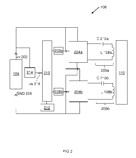
Referring now to Figure 2, there is illustrated schematically in more detail
the
circuitry 106 for the plurality of induction elements 108a, 108b for the
aerosol
generating device 100, according to an example.
The circuitry 106 comprises a plurality, in this example two, driver
arrangements 204a, 204b. Each driver arrangement 204a, 204b is electrically
connected to the battery 104. Specifically, each driver arrangement 204a, 204b
is
connected to a positive terminal of the battery 104, that provides relatively
high
electric potential +v 202, and to a negative terminal of the battery or to
ground, which
provides a relatively low or no or negative electric potential GND 206. A
voltage is
therefore established across each driver arrangement 204a, 204b.
Each driver arrangement 204a, 204b is electrically connected to a respective
LC circuit 205a, 205b. Each LC circuit 205a, 205b comprises a respective one
of the
induction elements 108a, 108b having inductance L, and a capacitor 210a, 210b
having capacitance C. In each LC circuit 205a, 205b, the induction element
108a,
108b and the capacitor 210a, 210b are connected in series.
CA 03121583 2021-05-31
WO 2019/122097 PCT/EP2018/086145
11
Each one of the plurality of driver arrangements 204a, 204b is arranged to
provide, from an input direct current from the battery 104, an alternating
current to a
respective one of the plurality of LC circuits 205a, 205b, and hence to a
respective
one of the plurality of induction elements 108a, 108b, in use. Each driver
arrangement
204a, 204b is connected in common to the DC power source or battery 104 to
provide
the input direct current in use.
Each driver arrangement 204a, 204b is electrically connected to a respective
driver controller 208a, 208b, for example comprising logic circuitry. Each
driver
controller 208a, 208b is arranged to control the respective driver arrangement
204a,
204b, or components thereof, to provide the output alternating current from
the input
direct current. Specifically, as described in more detail below, each driver
controller
208a, 208b may be arranged to control the provision of a switching potential
vs 216 to
one or more transistors of the respective driver arrangement 204a, 204b at
varying
times to cause the respective driver arrangement 204a, 204b to produce the
alternating
current.
Each driver controller 208a, 208b may be arranged to control the frequency of
alternating current provided to the respective LC circuit 205a, 205b and hence
the
frequency of the alternating current driven through the respective induction
element
108a, 108b. As mentioned above, LC circuits may exhibit resonance. Each driver
controller 208a, 208b may control the frequency of the alternating current
driven
through the respective LC circuit 205a, 205b (the drive frequency) to be at or
near the
resonant frequency of the LC circuit 205a, 205b. For example, the drive
frequency
may be in the MHz range, for example in the range 0.5 to 1.5 MHz for example 1
MHz. It will be appreciated that other frequencies may be used, for example
depending on the particular LC circuit 205a, 205b (and/or components thereof),
and/or susceptor 110 used. For example, it will be appreciated that the
resonant
frequency of the LC circuit 205a, 205b may be dependent on the inductance L
and
capacitance C of the circuit 205a, 205b, which in turn may be dependent on the
inductor 108a, 208b, capacitor 210a, 210b and susceptor 110 used.
CA 03121583 2021-05-31
WO 2019/122097 PCT/EP2018/086145
12
The circuitry 106 comprises a converter 214 arranged to step up an input
potential +v 202 to provide the switching potential vs 216 in use. That is,
the
switching potential vs 216 output by the converter 214 is higher or more
positive than
the electric potential +v 202 input to the converter 214. For example, the
converter
214 may be a DC-to-DC power converter, for example a boost converter (also
referred to as a step-up converter). For example, the boost converter may step-
up
voltage from its input (supply) to its output (load), while stepping down
current. For
example, the boost converter may be a switched-mode power supply (SMPS)
comprising two or more semiconductors, for example a diode and a transistor,
and one
or more energy storage elements, for example one or both of a capacitor and an
inductor, arranged for outputting a potential higher or voltage higher than an
input
potential or voltage. The amount by which the voltage is stepped-up or boosted
can be
fixed or variable, and may depend on a user input (e.g., a button or a
strength of a puff
as detected by a puff sensor (not shown)). The converter 214 is common to each
of the
plurality of driver arrangements 104a, 204b. That is the converter 214 is
arranged for
supplying the switching potential vs 216 to each of the plurality of driver
arrangements 204a, 204b in use. The converter 214 electrically connected to
the
battery 104, which provides the input potential +v 202 in use. Specifically,
the
converter is electrically connected to at least the positive terminal of the
battery 104
providing the input potential +v 202. The DC power source or battery 104 may
provide the input direct current in use and may also provide the input
potential +v 202
in use.
The circuitry 106 comprises a supply bus 210 for supplying the switching
potential vs 216 from the converter 214 to the driver controller 208a, 208b of
each
driver arrangement 204a, 204b. The supply bus 210 is controllable to supply
the
switching potential vs 216 to one or more of the plurality of driving
arrangements
204a, 204b. Specifically, the circuitry 106 comprises a supply bus controller
212
arranged to control the supply bus 210 to supply the switching potential vs
216 to a
selectable one or more of the plurality of driving arrangements 204a, 204b in
use, i.e.
to a selectable one or more of the driver controllers 208a, 208b of the
driving
CA 03121583 2021-05-31
WO 2019/122097 PCT/EP2018/086145
13
arrangements 204a, 204b in use. For example, the supply bus controller 212 may
control the supply bus 210 to supply the switching potential vs 216 to none of
the
driver arrangements 204a, 204b. In this case, none of the driver arrangements
204a,
204b may provide an alternating current to the respective induction elements
108a,
108b, and hence no inductive heating of the susceptor 110 may occur. As
another
example, the supply bus controller 212 may control the supply bus 210 to
supply the
switching potential vs 216 to a first 204a of the driver arrangements 204a,
204b, but
not to a second 204b of the driver arrangements. In this case, only the first
driver
arrangement 204a may provide an alternating current to the respective
induction
element 108a, and hence only a portion of the susceptor 110 may be inductively
heated. As another example, the supply bus controller 212 may control the
supply bus
210 to supply the switching potential vs 216 to both the first driver
arrangement 204a
and the second driver arrangements 204b. In this case, both the first driver
arrangement 204a and the second driver arrangement 204b may provide an
alternating
current to the respective induction elements 108a, 208b and hence a larger
portion of
susceptor 110 may be inductively heated, for example. In such a way, the
supply bus
210 and the supply bus controller 212 may provide for control over the
inductive
heating of the susceptor 110, and hence for example for control over the
heating of the
aerosol generating material (not shown in Figure 2) and hence for example for
control
over the aerosol generation of the overall aerosol generating device (not
shown in
Figure 2).
In use, when one or more of the driver controllers 208a, 208b is activated,
for
example when the supply bus controller 212 is controlled to supply the
switching
potential vs 216 to one or more of the driver controllers 208a, 208b, for
example by a
user, the or each driver controller 208a, 208b may control the respective
driver
arrangement 204a, 204b to drive alternating current through the respective LC
circuit
205a, 205b and hence through the respective induction element 108a, 108b,
thereby
inductively heating the susceptor 110 (which then may heat an aerosol
generating
material (not shown in Figure 2) to produce an aerosol for inhalation by a
user, for
example).
CA 03121583 2021-05-31
WO 2019/122097 PCT/EP2018/086145
14
Providing the converter 214 to supply the switching potential vs 216 needed to
switch the transistors of the driver arrangements 204a, 204b (which switching
potential is higher than the potential +v 202 provided by the battery 104, as
explained
in more detail below) removes the need to provide a separate DC power supply
or
battery for this purpose, and hence reduces the cost and complexity of the
circuitry
and hence overall aerosol generating device. Further, that the converter 214
is a global
converter, i.e. it is common to each of the plurality of driver arrangements
204a, 204b,
i.e. it provides the switching potential vs 216 for each of the plurality of
driver
arrangements 204a, 204b, removes the need for each driver arrangement 204a,
204b
to have its own individual local converter to provide the switching potential
vs 216 to
the driver arrangement 204a, 204b, and hence reduces the complexity and cost
of the
circuitry.
Referring now to Figure 3, there is illustrated schematically in more detail
one
of the driver arrangements 204a and its associated LC circuit 205a, according
to an
example. Each of the plurality of driver arrangements 204a, 204b described
above
with reference to Figure 2 may be the same as or similar to the example driver
arrangement 204a illustrated in Figure 3. It will be appreciated that in this
case, each
driver arrangement 204a, 204b will be arranged for driving its associated LC
circuit
205a, 205b comprising the associated induction element 108a, 108b.
The driver arrangement 204a comprises one or more transistors Ql, Q2, Q3,
Q4 controllable by the switching potential vs 216 to substantially allow
current to pass
therethrough in use. In the example illustrated in Figure 3, the driver
arrangement
204a comprises a plurality of transistors, specifically four transistors Ql,
Q2, Q3, Q4,
arranged in a H-bridge configuration (note that transistors arranged or
connected in a
H-bridge configuration may be referred to as a H-bridge). The H-bridge
configuration
comprises a high side pair 304 of transistors Ql, Q2 and a low side pair 306
of
transistors Q3, Q4. A first transistor Q1 of the high side pair 304 is
electrically
adjacent to a third transistor Q3 of the low side pair 306, and a second
transistor Q2 of
the high side pair 304 is electrically adjacent to a fourth transistor Q4 of
the low side
pair 314. The high side pair 304 are for connection to a first electric
potential +v 202
CA 03121583 2021-05-31
WO 2019/122097 PCT/EP2018/086145
higher than a second electric potential GND 206 to which the low side pair 306
are for
connection. In this example, the driver arrangement 204a is arranged for
connection
of the DC power source 104 (not shown in Figure 3) across a first point 322
between
the high side pair 304 of transistors Ql, Q2 and a second point 320 between
the low
5 side pair 306 of transistors Q3, Q4. Specifically, the first point 322 is
for connection
to a positive terminal of the battery (not shown) and the second point 320 is
for
connection to a negative terminal of the battery (not shown) or ground. In use
therefore, a potential difference is established between the first point 322
and the
second point 320.
As with Figure 2, the driver arrangement 204a illustrated in Figure 3 is
electrically connected to, and arranged to drive, the LC circuit 208a
comprising the
induction element (not shown in Figure 3). Specifically, the induction element
(as part
of the LC circuit 208) is connected across a third point 324 between one of
the high
side pair of transistors Q2 and one of the low side pair of transistors Q4 and
a fourth
point 326 between the other of the high side pair of transistors Q1 and the
other of low
side second pair of transistors Q3.
Each transistor Ql, Q2, Q3, Q4 is a field effect transistor controllable by
the
switching potential vs 216 to substantially allow current to pass therethrough
in use.
Each field effect transistor Ql, Q2, Q3, Q4 comprises a source S, a drain D,
and a
gate G. The switching potential is provided to the gate of each field effect
transistor,
which as described above may allow current to pass between the source S and
the
drain D of each field effect transistor Ql, Q2, Q3 Q4. Accordingly, each field
effect
transistor Ql, Q2, Q3, Q4 is arranged such that, when the switching potential
is
provided to the field effect transistor Ql, Q2, Q3, Q4 then the field effect
transistor
Ql, Q2, Q3, Q4, substantially allows current to pass therethrough, and when
the
switching potential is not provided to the field effect transistor Ql, Q2, Q3,
Q4, then
the field effect transistor Ql, Q2, Q3, Q4 substantially prevents current from
passing
therethrough. In the example illustrated in Figure 3, each field effect
transistor Ql,
Q2, Q3, Q4 has an associated switching potential line or connection 311, 312,
313,
314 (respectively) for carrying the switching potential thereto.
CA 03121583 2021-05-31
WO 2019/122097 PCT/EP2018/086145
16
The associated driver controller (not shown in Figure 3a, but see the driver
controller 208a in Figure 2) is arranged to control supply of the switching
potential to
each field effect transistor Ql, Q2, Q3, Q4. Specifically, the driver
controller is
arranged to control the supply of the switching potential vs 216 to each
supply line or
connection 311, 312, 313, 314 independently, thereby to independently control
whether each respective transistor Q 1, Q2, Q3, Q4 is in an "on" mode (i.e.
low
resistance mode where current passes therethrough) or an "off' mode (i.e. high
resistance mode where substantially no current passes therethrough).
By controlling the timing of the provision of the switching potential to the
respective field effect transistors Q 1, Q2, Q3, Q4, the driver controller
208a may
cause alternating current to be provided to the associated LC circuit 205a,
and hence
for alternating current to be provided to the associated induction element
(not shown
in Figure 3a) thereof. For example, at a first time, the driver controller
208a may be in
a first switching state, where a switching potential is provided to the first
and the
fourth field effect transistors Ql, Q4, but not provided to the second and the
third field
effect transistors Q2, Q3. Hence the first and fourth field effect transistors
Ql, Q4 will
be in a low resistance mode, whereas second and third field effect transistors
Q2, Q3
will be in a high resistance mode. Therefore, at this first time, current will
flow from
the first point 322 of the driver arrangement 204a, through the first field
effect
transistor Q 1, through the LC circuit 205a in a first direction (left to
right in the sense
of Figure 3), through the fourth field effect transistor Q4 to the second
point 320 of
the driver arrangement 204a. However, at a second time, the driver controller
208a
may be in a second switching state, where a switching potential is provided to
the
second and third field effect transistors Q2, Q3, but not provided to the
first and the
fourth field effect transistors Q 1, Q4. Hence the second and third field
effect
transistors Q2, Q3 will be in a low resistance mode, whereas first and fourth
field
effect transistors Q 1, Q4 will be in a high resistance mode. Therefore, at
this second
time, current will flow from the first point 322 of the driver arrangement
204, through
the second field effect transistor Q2, through the LC circuit 205a in a second
direction
opposite to the first direction (i.e. right to left in the sense of Figure 3),
through the
CA 03121583 2021-05-31
WO 2019/122097 PCT/EP2018/086145
17
third field effect transistor Q3 to the second point 320 of the driver
arrangement 204.
By alternating between the first and second switching state therefore, the
driver
controller 208a may control the driver arrangement 204a to provide (i.e.
drive)
alternating current through the LC circuit 205a and hence through the
induction
element 108a. It will be appreciated that the same control scheme may be
employed
by the other driver controller 208b for the other driver arrangement 204b
associated
with the other induction element 108b of the other LC circuit 205b.
At least one of the high side pair of transistors Ql, Q2 is an n-channel field
effect transistor, for example an enhancement mode n-channel metal-oxide-
semiconductor field effect transistor. Specifically, in this example, both of
the high
side pair of transistors Ql, Q2 are n-channel field effect transistors.
Similarly, in this
example, both of the low side pair of transistors Q3, Q4 are n-channel field
effect
transistors, for example enhancement mode n-channel metal-oxide-semiconductor
field effect transistors.
As also described above, for n-channel FETs, the drain terminal D is placed at
a higher potential than the source terminal S (i.e. there is a positive drain-
source
voltage, or in other words a negative source-drain voltage), and in order to
turn the n-
channel FET "on" (i.e. to allow current to pass therethrough), the switching
potential
applied to the gate terminal G needs to be is higher than the potential at the
source
terminal S. Since the high side pair 304 of transistors Ql, Q2 are n-channel
field
effect transistors, at certain times during operation of the driver
arrangement 204a, the
potential experienced at the source terminal S of those n-channel filed effect
transistors Ql, Q2 is +v 202. Therefore, the switching potential vs 216
provided to the
gates G of those transistors in order to turn them on needs to be higher than
+v 202,
(i.e. higher than the potential provided by the positive terminal of the DC
power
source 104). The converter 214 provides, via the supply bus 210 and the driver
controller 208a, such a switching potential vs 216 to the high side n-channel
filed
effect transistors Ql, Q2, thereby allowing appropriate operation of those
transistors.
CA 03121583 2021-05-31
WO 2019/122097 PCT/EP2018/086145
18
For the low side pair 306 of n-channel field effect transistors Q3, Q4, the
potential experienced at their source terminals S will be GND 206. Hence for
the low
side pair 306 of n-channel field effect transistors Q3, Q4, the switching
potential
applied to their gate terminal G to turn them "on" need not necessarily be
higher than
+v 202, and may be any potential higher than GND 206. Nonetheless, the
switching
potential vs 202 used for the high side pair 304 of n-channel field effect
transistors
Q 1, Q2 can also be used for the low side pair 306 of n-channel field effect
transistors
Q3, Q4, as this switching potential vs 216 is higher than GND 206. The
switching
potential vs 216 provided by the converter 214 common to each of the plurality
of
driver arrangements 204a, 204b can therefore be used as the switching
potential vs
216 for each of the n-channel field effect transistors Q 1, Q2, Q3, Q4 of each
of the
driver arrangements 204a, 204b, hence reducing the complexity and hence cost
of the
circuitry, for example as compared to providing separate converters for each
driver
arrangement 204a, 204b, or for example as compared to providing different
switching
voltages for different ones of the transistors Q 1, Q2, Q3, Q4 of each driver
arrangement 204a, 204b.
As mentioned above, n-channel FETs such as n-MOSFETs typically have a
relatively low source-drain resistance generates relatively little heat in use
and hence
wastes relatively little energy in operation. The use of an n-channel FET such
as an n-
MOSFET as one or more (or each) of the transistors Q 1, Q2, Q3, Q4 of a driver
arrangement 204a, 204b may therefore provide for efficient operation.
Further, as mentioned above, n-channel FETs such as n-MOSFETs typically
have relatively short switching times (e.g. a characteristic response time
from
changing the switching potential provided to the gate terminal G to the FET
changing
whether or not current passes therethrough), which can allow for relatively
high
switching rates. For example, the turn off delay time for an n-MOSFET may be
70 ns.
The use of an n-channel FET such as an n-MOSFET as one or more (or each) of
the
transistors Q 1, Q2, Q3, Q4 of a driver arrangement 204a, 204b may therefore
provide
for the associated induction elements 108a, 108b to be driven at relatively
high
frequencies, which may for example provide for more flexible operation.
CA 03121583 2021-05-31
WO 2019/122097 PCT/EP2018/086145
19
Further, during the operation of each driver arrangement 204a, 204b, there
may be a short time when both the first transistor Q1 of the high side pair
304 and the
third transistor Q3 of the low side pair (or both the second transistor Q2 of
the high
side pair 304 and the fourth transistor Q4 of the low side pair) are open or
"on", at
which point a significant amount of current can be momentarily conducted
through
the driver arrangement 204a, 204b without passing through the induction
element
108a, 108b. This loss is referred to as "shoot-through", and may occur twice
per
cycle. The shoot-through loss may become higher at higher switching
frequencies
(lower switching periods), for example when the switching period becomes
comparable to the switching time of the transistors. The use of an n-channel
FET such
as an n-MOSFET (which have relatively short switching times) as one or more
(or
each) of the transistors Q 1, Q2, Q3, Q4 of a driver arrangement 204a, 204b
may
therefore provide for the minimisation of shoot-through loss, and hence
provide for a
.. more efficient operation.
In the above example, each of the transistors Q 1, Q2, Q3, Q4 of each driving
arrangement 204a, 204b were n-channel field effect transistors. However, it
will be
appreciated that this need not necessarily be the case and that in other
examples each
driver arrangement 204a, 204b may comprise one or more first transistors each
controllable by a switching potential provided by the converter 214 to
substantially
allow current to pass through that transistor in use. The cost and/or
complexity
reduction benefit of the converter 214 being common to each of the plurality
of driver
arrangements 204a, 204 may nonetheless be provided.
In the above examples, each driver arrangement 204a, 204b comprised four
transistors Q 1, Q2, Q3, Q4 arranged in a H-bridge configuration but it will
be
appreciated that in other examples one or more of the driver arrangements
204a, 204b
may comprise further transistors, that may or may not be part of the H-bridge
configuration.
CA 03121583 2021-05-31
WO 2019/122097 PCT/EP2018/086145
Although in the above examples, the field effect transistors Ql, Q2, Q3, Q4
were depletion mode metal-oxide field effect transistors, it will be
appreciated that
this need not necessarily be the case and that in other examples other types
of field
effect transistors may be used.
5
The above examples are to be understood as illustrative examples of the
invention. It is to be understood that any feature described in relation to
any one
example may be used alone, or in combination with other features described,
and may
also be used in combination with one or more features of any other of the
examples,
10 or any combination of any other of the other examples. Furthermore,
equivalents and
modifications not described above may also be employed without departing from
the
scope of the invention, which is defined in the accompanying claims.