Note: Descriptions are shown in the official language in which they were submitted.
ASYMMETRIC LATERAL AVALANCHE PHOTODETECTOR
BACKGROUND
The present disclosure relates to lateral avalanche photodetectors. In
some aspects, the present disclosure relates to deep-level doped lateral
silicon
avalanche photodetectors.
The avalanche photodetector (APD) is a widely deployed semiconductor
device used for the detection of optical signals with relatively low power. By
application of a large electric field, primary photocarriers in the device can
be
accelerated such that they create additional carriers in an "avalanche"
effect. The
most commonly used material for the fabrication of APDs is silicon.
SUMMARY
Avalanche photodetector devices are disclosed in which spatial
asymmetry is employed to preferentially enhance avalanche multiplication of
electrons. In some example embodiments, an avalanche photodetector device
includes p-doped and n-doped regions and a central waveguide region, where
the p-doped region is laterally offset from the central waveguide by a first
lateral
offset region, and where the n-doped region is laterally offset from the
central
waveguide by a second lateral offset region. The first and second lateral
offset
regions are asymmetrically defined such that impact ionization and avalanche
multiplication of electrons in the second laterally offset region is enhanced
relative to that of holes in the first laterally offset region. In some
example
1
Date Recue/Date Received 2021-06-17
implementations, the asymmetry may be provided by a difference in relative
heights and/or lateral spatial extends (widths) of the lateral offset regions,
such
that the electric field, or a spatial extent associated therewith, is enhanced
for
electrons.
A further understanding of the functional and advantageous aspects of the
disclosure can be realized by reference to the following detailed description
and
drawings.
BRIEF DESCRIPTION OF THE DRAWINGS
Embodiments will now be described, by way of example only, with
reference to the drawings, in which:
FIG. 1A shows a cross-sectional view of a symmetric avalanche
photodetector device.
FIG. 1B shows various spatial measures within a cross-section taken
through the symmetric avalanche photodetector device.
FIG. 1C plots the electric field within a cross-section taken through the
symmetric avalanche photodetector device when the device is reverse biased.
FIG. 2A shows a cross-sectional view of an asymmetric avalanche
photodetector device having a height asymmetry on either side of the central
waveguide region.
FIG. 2B shows various spatial measures within a cross-section taken
through the asymmetric avalanche photodetector device having a height
asymmetry on either side of the central waveguide region.
2
Date Recue/Date Received 2021-06-17
FIG. 2C plots the electric field within a cross-section taken through the
asymmetric avalanche photodetector device having a height asymmetry on either
side of the central waveguide region when the device is reverse biased.
FIG. 3A shows a cross-sectional view of an asymmetric avalanche
photodetector device having a lateral asymmetry of the n+ and p+ regions
relative to the central waveguide region.
FIG. 3B shows various spatial measures within a cross-section taken
through the asymmetric avalanche photodetector device having a lateral
asymmetry of the n+ and p+ regions relative to the central waveguide region.
FIG. 3C plots the electric field within a cross-section taken through the
asymmetric avalanche photodetector device having a lateral asymmetry of the n+
and p+ regions relative to the central waveguide region when the device is
reverse biased.
FIG. 4 plots the electric field along the lateral dashed paths shown in
FIGS. 1C, 2C and 3C.
FIG. 5 plots the impact generation rate along the lateral dashed paths
shown in FIGS. 1C, 2C and 3C.
FIG. 6 plots the electron ionization coefficient along the lateral dashed
paths shown in FIGS. 1C, 2C and 3C.
DETAILED DESCRIPTION
Various embodiments and aspects of the disclosure will be described with
reference to details discussed below. The following description and drawings
are
3
Date Recue/Date Received 2021-06-17
illustrative of the disclosure and are not to be construed as limiting the
disclosure.
Numerous specific details are described to provide a thorough understanding of
various embodiments of the present disclosure. However, in certain instances,
well-known or conventional details are not described in order to provide a
concise discussion of embodiments of the present disclosure.
As used herein, the terms "comprises" and "comprising" are to be
construed as being inclusive and open ended, and not exclusive. Specifically,
when used in the specification and claims, the terms "comprises" and
"comprising" and variations thereof mean the specified features, steps or
components are included. These terms are not to be interpreted to exclude the
presence of other features, steps or components.
As used herein, the term "exemplary" means "serving as an example,
instance, or illustration," and should not be construed as preferred or
advantageous over other configurations disclosed herein.
As used herein, the terms "about" and "approximately" are meant to cover
variations that may exist in the upper and lower limits of the ranges of
values,
such as variations in properties, parameters, and dimensions. Unless otherwise
specified, the terms "about" and "approximately" mean plus or minus 25 percent
or less.
It is to be understood that unless otherwise specified, any specified range
or group is as a shorthand way of referring to each and every member of a
range
or group individually, as well as each and every possible sub-range or sub-
group
encompassed therein and similarly with respect to any sub-ranges or sub-groups
4
Date Recue/Date Received 2021-06-17
therein. Unless otherwise specified, the present disclosure relates to and
explicitly incorporates each and every specific member and combination of sub-
ranges or sub-groups.
As used herein, the term "on the order of", when used in conjunction with
a quantity or parameter, refers to a range spanning approximately one tenth to
ten times the stated quantity or parameter.
Unless defined otherwise, all technical and scientific terms used herein
are intended to have the same meaning as commonly understood to one of
ordinary skill in the art. Unless otherwise indicated, such as through
context, as
used herein, the following terms are intended to have the following meanings:
As used herein, the phrase "deep level" pertains to the energy level of a
dopant or defect for which the energy level separation relative to a band edge
is
at least 3 times kT, where k is Boltzman's constant and T is temperature.
While silicon APDs are known for use in above-bandgap operation, the
implantation of silicon with deep levels permits absorption of sub-bandgap
light,
facilitating the functioning of a deep-level-implanted silicon material as a
photodetector. For example, Ackert et al. (Ackert et al., Opt. Express 21,
19530-
1957, 2013) has described a deep-level-implanted waveguide silicon avalanche
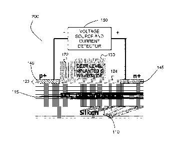
photodiode, which is schematically illustrated in FIG. 1A.
The Ackert device 100 employs a silicon-on-insulator structure, as shown
in the figure, in which a silicon substrate 110 supports a SiO2 insulator
layer 115,
upon which a top silicon device layer 120 is provided. The central silicon
waveguide 130 region is formed on the silicon device layer 120. The silicon
5
Date Recue/Date Received 2021-06-17
waveguide 130 is doped with deep level impurities (e.g. substitutional
impurities
or lattice defects) that facilitates the excitation of photocarriers via the
absorption
of sub-bandgap light.
As shown in the figure, p+ and n+ regions 140 and 145 are respectively
provided on opposites sides of waveguide 130, in a manner suitable for
applying
an electric field within waveguide 130. The adjacent p+ and n+ regions 140 and
145, and silicon waveguide 130, together form a p-i-n junction (the
"intrinsic"
region being doped/implanted with deep level impurities). Metal electrodes
(not
shown) may be respectively formed over (or otherwise be brought into
electrical
communication with) the p+ and n+ regions 140 and 145, and the electrodes may
be contacted, for example via bonded wires, to electrical circuitry 150 that
includes, for example, a voltage source for generating a reverse bias
(potential
difference) and a current detector (e.g. amplifier circuit). The applied
reverse bias
applied to the Ackert device 100 is sufficient to support impact ionization of
both
electrons and holes.
FIG. 1B shows a cross-sectional view of the silicon device layer and the
optical mode that is axially guided within the waveguide. Photons are absorbed
within the low-doped or intrinsic region and electron-hole pairs are created
commensurate with the waveguide mode (approximated by the circular region).
As can be seen in FIGS. 1A and 1B, the Ackert device includes intrinsic offset
regions 122 and 124 that laterally offset the respective p+ and n+ regions 124
and 124 from the central waveguide region 130. These lateral offset regions
facilitate the generation of secondary carriers (avalanche multiplication) via
6
Date Recue/Date Received 2021-06-17
impact ionization.
FIG. 1C plots the electric field within a cross-sectional region of a device
having a 90 nm P-type slab height, a 90 nm N-type slab height, a 1 pm ridge
width, and a 220 nm ridge height. The electric field extends within the
lateral
offset regions 122 and 124 when the device is reverse biased, such that photo-
generated carriers drift toward the p+ and n+ regions 122 and 124. Under
sufficiently strong electric fields, avalanche carrier generation takes place,
significantly increasing the photocurrent. Both holes and electrons are
generated
and both are subjected to the avalanche process, creating additional carriers
at a
rate related to their ionization coefficients. It is noted that in silicon,
the ionization
coefficient of electrons is larger than holes, while these coefficients
increase with
electric field and become less dissimilar as the electric field increases.
As can be clearly seen in FIGS. 1A-1C, the Ackert device is spatially
symmetric relative to the central waveguide region. As a consequence, the
primary carrier injection into the higher field lateral offset regions of the
APD
takes place via both electrons and holes, which are subjected to essentially
the
same electric field strength. The present inventors realized that such a
configuration is not ideal from the viewpoint of excess noise generation and
device bandwidth, understanding that in order to achieve improved noise
performance, the ionization coefficients of the primary carriers should be as
different as possible and the avalanche process should be predominantly
initiated by the carrier species with the higher ionization rate. The present
inventors thus realized improved silicon-based APD devices could be achieved
7
Date Recue/Date Received 2021-06-17
by employing a design that promotes impact ionization via electrons rather
than
holes via an asymmetric spatial configuration.
An example embodiment of a spatially asymmetric deep-level implanted
silicon waveguide APD is shown in FIGS. 2A-2C. As shown in the figures,
spatial
asymmetry is achieved by increasing the height (thickness) of the lateral
offset
region 122 on the p+ side of the waveguide region 130, which reduces the
electric field on the p+ side of the waveguide region 130 and enhances the
electric field within the lateral offset region 124 on the n+ side of the
device. The
reduction of the electric field within the p+ side lateral offset region 122
reduces
or suppress impact ionization via injected holes, while the increase in the
electric
field within the lateral offset region 124 on the n+ side of the device
enhances
impact ionization (and secondary carrier generation) via the injected
electrons.
Accordingly, such a device configuration leads to improved noise performance
relative to its symmetric counterpart of FIGS. 1A-1C.
The reverse bias may be applied such that a threshold of avalanche
multiplication is achieved for electrons without achieving a threshold of
avalanche
multiplication for holes. The skilled artisan may experiment with different
height
ranges of the p+ side and n+ side lateral offset regions 122 and 124, for a
given
reverse bias and waveguide configuration, in order to identify suitable
respective
heights that result in preferential avalanche multiplication of electrons. The
present inventors have found, for example, that a suitable reverse bias is one
that results in an electric field within a range of 1x10⁵ to 1x10⁶ V/cm within
the n+
side lateral offset region, when the APD is fabricated using silicon.
8
Date Recue/Date Received 2021-06-17
As shown in FIG. 2B, the spatial asymmetry that leads to preferential
electron impact ionization and avalanche multiplication is achieved via the
differences in heights of the hp+slab > hN+slab- It will be understood that
the larger
the ratio of hp +slab. ¨ lh
N+slab, the greater the asymmetry in field strength in the two
slabs will be. As hm-siab decreases, the risk of damage to the material from
excessive current density may increase.
As hP+slab becomes close in height to hridge, the center of the optical mode
will tend to extend toward the p+ side, as illustrated in FIG. 2B. As a
consequence, the photogenerated carriers are created toward the p+ side,
introducing further asymmetry. This modal asymmetry provides a second
mechanism that favours enhanced avalanche multiplication of photogenerated
electrons by providing an increased distance over which electrons travel
toward
the n+ region, compared to the distance traveled by holes to the p+ region,
thus
promoting a higher probability for impact ionization of electrons to occur.
In some example implementations, the height asymmetry of the lateral
offset regions 122 and 124 may be provided such that hP+slab is no greater
than
0.99*hridge and hm-siab is greater than 0.01 *hridge. The width of the central
region,
Wridge should be sufficiently large to confine the optical mode horizontally,
while
being sufficiently small enough to promote high enough electric fields at
reasonable voltages. In some example implementations, the central waveguide
region may be defined such that 10*A > hridge> 0.025*A and 10*A > Wridge >
0.025*A, where A is an operating wavelength of the device.
The lateral spatial extent of the p+ side lateral offset region 122 may be
9
Date Recue/Date Received 2021-06-17
selected such that a suitable reduction in the electric field within the p+
side
lateral offset region 122 prevents an onset of avalanche multiplication of
holes,
while facilitating the avalanche multiplication of electrons, within the n+
side
lateral offset region 124, for a given applied reverse bias or reverse bias
range.
In some example implementations, the spatial extent of the lateral offset
region
122 may be between 50 and 100 nm, between 50 and 200 nm, or between 100
and 200 nm. In some example implementations, the lateral extent of the p+ side
lateral offset region may be sufficiently small such that parasitic absorption
of
light guided by said silicon waveguide and having a wavelength of 1500 nm is
less than 10%.
FIG. 2C plots the electric field within a cross-section taken through an
asymmetric avalanche photodetector having a height asymmetry of the lateral
offset regions 122 and 124 under reverse bias. The device was modeled with a
200 nm P-type slab height, a 50 nm N-type slab height, a 1 pm ridge width, and
220 nm ridge height. As can be seen by comparison with FIG. 1C, the increased
height of the lateral offset region 122 on the p+ side leads to a reduction of
the
electric field within this region, while the decreased height of the lateral
offset
region on the n+ side leads to an increased electric field, thereby promoting
increased impact ionization and avalanche multiplication of electrons relative
to
holes.
Another example embodiment that employs spatial asymmetry is
illustrated in FIGS. 3A-3C, in which the spatial asymmetry that confers
enhanced
impact ionization and avalanche multiplication of electrons is provided in the
Date Recue/Date Received 2021-06-17
lateral direction. As shown in the figures, p+ side lateral offset region 122
is less
than the n+ side lateral offset region 124, such that dp+slab < dN+slab, and
such that
the n+ region 145 is further from the central waveguide region 130 than the p+
region 140. Accordingly, photogenerated electrons will encounter the electric
field
over a longer distance than the photogenerated holes under reverse bias,
promoting a higher probability for impact ionization of electrons to occur
relative
to holes.
The reverse bias may be applied such that a threshold of avalanche
multiplication is achieved for electrons without achieving a threshold of
avalanche
multiplication is achieved for holes. The skilled artisan may experiment with
different lateral extent ranges of the p+ side and n+ side lateral offset
regions 122
and 124, for a given reverse bias and waveguide configuration, in order to
identify suitable respective lateral extents that result in preferential
avalanche
multiplication of electrons.
In some example embodiments, the p+ side lateral offset region 122 may
be less than 100 nm, less than 50 nm, less than 20 nm, or zero. The choice of
a
suitable lateral extent of the p+ side lateral offset region 122 may depend on
the
modal confinement of the optical mode within the central waveguide region,
with
the lateral extent of the p+ side lateral offset region being selected to
avoid or
reduce parasitic absorption of the guided optical mode. Fore example, in large
cross-section waveguides, it may be possible for the p+ region 140 to be very
close to the central waveguide region 130 without leading to significant
parasitic
absorption. For example, this may be the case when hN+siab and hP+slab are
11
Date Recue/Date Received 2021-06-17
approximately less than half of hridge-
In some example implementations, the lateral extent of the n+ side lateral
offset region 124 is 1.1 times to 10 times longer than the lateral extent of
the p+
side lateral offset region 122. In some example implementations, the n+ offset
region 124 is larger than the p+ offset region 22 by at least 100 nm while
maintaining a lateral spatial extent that is sufficiently small to maintain an
electric
field above an avalanche threshold (e.g. -105 V/cm) for a given reverse bias
voltage, such as maximum lateral spatial extend of 1000 nm.
FIG. 3C plots the electric field within a cross-section taken through an
asymmetric avalanche photodetector having a height asymmetry of the lateral
offset regions 122 and 124 under reverse bias. The device was modeled with a
90 nm P-type slab height, 90 nm N-type slab height, 1 pm ridge width, 220 nm
ridge height. As can be seen by comparison with FIG. 1C, the increased length
of
the lateral offset region 124 on the n+ side leads to an increased interaction
length of the injected electrons with the electric field relative to the p+
lateral
offset region 122, thereby promoting increased impact ionization and avalanche
multiplication of electrons relative to holes.
Referring now to FIG. 4, the electric field is plotted along the contours 160,
161 and 162 in FIGS. 2C, 3C and 4C, respectively, for the cases of a symmetric
device, a device with height asymmetry in the lateral offset regions, and a
device
with asymmetry in the lateral extent of the lateral offset regions. The
symmetric
device shows a symmetric electric field profile with higher field
concentrations
toward the edges of the P+ and N+ contacts due to the larger potential across
12
Date Recue/Date Received 2021-06-17
the thinner slab regions. However, the asymmetric device with an asymmetry in
the relative heights of the lateral offset regions 122 and 124 shows increased
electric field toward the N+ region and reduced electric field toward the P+
region
due to the difference in potentials across the respectively thinner and
thicker slab
regions. The asymmetric device with an asymmetry in the relative lateral
extents
of the lateral offset regions 122 and 124 shows an extension of a high
electric
field on the N+ side (relative to the P+ side) due to the wider slab region
(WN-E-
slab). As can be seen in the figure, even though the electric field amplitude
is
higher on the p+ side of the device for the case of an asymmetric device with
an
asymmetry in the relative lateral extent of the lateral offset regions 122 and
124,
the electric field within the extended n+ lateral offset region 124 has an
increased
value, relative to the central waveguide region, over a much longer lateral
extent
than the corresponding p+ lateral offset region 122, thereby supporting the
preferential avalanche multiplication of injected electrons.
FIG. 5 plots the impact ionization rate along the contours 160, 161 and
162 in FIGS. 2C, 3C and 4C, respectively, for the cases of a symmetric device,
a
device with height asymmetry in the lateral offset regions, and a device with
asymmetry in the lateral extents of the lateral offset regions. The symmetric
device shows an asymmetric impact generation rate toward the N+ contacts due
to the naturally higher electron ionization coefficient as compared with the
hole
ionization coefficient. The impact generation rate is strongly correlated with
the
electric field strength. However, the asymmetric device with an asymmetry in
the
relative heights of the lateral offset regions 122 and 124 shows an enhanced
13
Date Recue/Date Received 2021-06-17
impact generation rate toward the N+ region due to the higher electric field
toward the N+ side as described previously. The reduced electric field toward
the
P+ region conversely decreases the impact generation rate in this region. The
asymmetric device with an asymmetry in the relative lateral extents of the
lateral
offset regions 122 and 124 shows an elongated region of high impact generation
rate due to the wider slab region toward the N+ region.
FIG. 6 plots the electron ionization coefficient along the contours 160, 161
and 162 in FIGS. 2C, 3C and 4C, respectively, for the cases of a symmetric
device, a device with height asymmetry in the lateral offset regions, and a
device
with asymmetry in the lateral extents of the lateral offset regions. The
symmetric
device shows a higher electron ionization coefficient toward the N+ side
relative
to the P+ side due to the drift of electrons toward the N+ region. The reduced
ionization coefficients toward the P+ side demonstrate that electrons are
being
generated here from impact ionization but do not avalanche strongly in this
region as they drift toward the N+ region, passing through the intrinsic
region
where the field is lower. However, the asymmetric device with an asymmetry in
the relative heights of the lateral offset regions 122 and 124 shows a
strongly
increased electron ionization coefficient in the N+ region corresponding to
the
higher electric field. As mentioned previously these coefficients are field-
.. dependent. The asymmetric device with an asymmetry in the relative lateral
extents of the lateral offset regions 122 and 124 shows an elongated region of
high electron ionization coefficient corresponding to the longer slab region.
Deep levels may be generated within the silicon waveguide by ion
14
Date Recue/Date Received 2021-06-17
implantation, which is a common fabrication process in the semiconductor
industry. Chemically inert ions (such as hydrogen, helium, nitrogen, argon,
silicon, germanium); or ions that could be chemically active if subjected to a
post
ion implantation high temperature anneal in excess of 800K (such as boron,
phosphorus, arsenic) may be accelerated, for example, to an energy of between
1 and 4000 keV, and penetrate the silicon, creating lattice defects (which are
electrical deep-levels typically greater than 3 times kT in energy from either
the
conduction or valence band, where K is Boltzmann's constant and T is
temperature) through collisions with lattice atoms. The number of deep levels
and their position depends on the energy, dose and mass of the accelerated
ions. In some example implementations, ion implantation may be followed by a
low-temperature (e.g. up to 600K) thermal treatment which may increase the
sensitivity of the waveguide to sub-bandgap photons. Deep levels may also be
introduced via low-temperature (less than 600K) deposition of material which
may form the waveguide. Deep levels may also be introduced by subjecting the
waveguide to an inert plasma process. In some example implementations, the
concentration of deep levels within the central waveguide region may be
between
1x1014 cm-3 and 1x1019 cm-3.
Although the preceding example embodiments describe the central
waveguide region as including deep levels to facilitate absorption of sub-
bandgap
light, it will be understood that at least the n+ side lateral offset region
110 may
also be doped to include deep levels. The presence of deep levels in the n+
lateral offset region may provide an increased probability (cross-section) for
Date Recue/Date Received 2021-06-17
electron impact ionization, further enhancing electron avalanche
multiplication
relative to hole avalanche multiplication. According to some example methods,
deep levels may be generated within n+ lateral offset region for which
ionization
is preferentially initiated by electrons. Examples of such deep levels include
the
divacancy, vacancy-impurity complexes (such as oxygen-vacancy, carbon-
vacancy, boron-vacancy, phosphorus-vacancy), interstitial clusters of between
1
and several million atoms, dislocations, clusters of vacancies between 2 and
several million vacancies.
In some example implementations, apart from the presence of deep
levels, the lateral offset regions and central waveguide regions may be
otherwise
intrinsic (absent of shallow dopants) or include shallow dopants at
concentrations
less than 1x1019 cm-3. In other example implementations, a portion of the
lateral
offset region 122 that is closer to the central waveguide region than the n+
region
may be doped with a concentration of p-type dopants having a concentration
that
is less that a concentration of p-type dopants within the p+ region. This p
region
effectively reduces the potential drop of the reverse bias over the p+ side
lateral
offset region 124 and the central waveguide region while increasing the
electric
field within the remaining portion of the n+ side lateral offset region,
thereby
preferentially enhancing electron avalanche multiplication.
The preceding example embodiments have separately illustrated the use
of unidirectional asymmetry in (i) the height of the lateral offset regions
and (ii)
the lateral spatial extent of the lateral offset regions. In the example
embodiment
shown in FIGS 2A-2C, the lateral extents of the lateral offset regions 122 and
16
Date Recue/Date Received 2021-06-17
124 are equal, as in the symmetric device shown in FIGS. 1A-1C, with the
device
asymmetric occurring due to the different heights (thicknesses) of the two
lateral
offset regions 122 and 124. Due to the asymmetric design, the electric field
is
stronger with the lateral offset region on the n+ side of the waveguide,
compared
to the electric field within the lateral offset region 122 on the p+ side,
such that
electrons subjected to a much larger field, with avalanche multiplication
being
dominated by electrons. In the example embodiment illustrated in FIGS. 3A-3C,
the heights the lateral offset regions 122 and 124 are equal, as in the
symmetric
device shown in FIGS. 1A-1C, with the device asymmetric occurring due to the
different lateral extents of the lateral offset regions 122 and 124. Due to
the
asymmetric design, the electric field extends over a longer lateral region
within
the lateral offset region 124 on the n+ side of the waveguide, compared to the
lateral offset region 122 on the p+ side, such that electrons are subjected to
an
electric field over a longer interaction length, enabling avalanche
multiplication to
.. be dominated by electrons.
It will be understood, however, that asymmetry that favours electron
avalanche multiplication and improved noise performance may be provided in
two dimensions. For example, the asymmetry may be present in both the height
and the lateral extent of the lateral offset regions 122 and 124, such that
the
height of the p+ side lateral offset region 122 is larger than the height of
the n+
side lateral offset region 124, and such that the lateral extent of the n+
side
lateral offset region 124 is larger than the lateral extent of the p+ side
lateral
offset region 122, with the n+ region 145 being further from the central
17
Date Recue/Date Received 2021-06-17
waveguide region 130 than the p+ region 140. Such an example implementation
may be beneficial in both enhancing the electric field and extending the
spatial
region over which impact ionization occurs, within the n+ side of the device
where electron impact ionization occurs, thus leading to enhanced electron
avalanche multiplication and supressed or eliminated hole avalanche
multiplication. The reverse bias may be applied such that a threshold of
avalanche multiplication is achieved for electrons without achieving a
threshold of
avalanche multiplication is achieved for holes.
It is to be understood that the ridge waveguide/S01 configuration shown in
FIGS. 2A and 3A are provided as non-limiting examples, and that other
configurations are possible, provided that the waveguide is doped with deep
level
impurities, includes at least one guided mode at a sub-bandgap wavelength. For
example, in other embodiments, the central waveguide may be provided in the
form of a rib waveguide, a buried waveguide, and air bridge waveguide.
While the preceding example embodiments have described waveguide
avalanche photodetectors formed from a silicon device layer, in other example
implementations, the semiconductor may be a semiconductor other than silicon,
provided that a suitable deep level dopant is provided. Suitable examples of
semiconductors and associated deep level dopants include, but are not limited
to, germanium doped with sulfur or gallium arsenide doped with nickel, tin or
cobalt.
In some example implementations, an avalanche photodiode device
according to the previously described embodiments may be integrated in
18
Date Recue/Date Received 2021-06-17
photonic systems which require an electrical response to the presence of
light,
whether as a terminal detector in a receiver system, a terminal detector at
the
end of a tap measuring a small portion of the light present in a waveguide or
as
an in-line tap detector.
Furthermore, avalanche photodiode devices according to the previously
described embodiments may be incorporated into resonant structures, such as
micro-ring resonators and Fabry-Perot cavities which may act to sensitize the
avalanche photodetector in a spectrally-selective manner. Grating structures
may
be etched into the silicon to provide the reflections necessary to construct a
resonant cavity but may also be implemented through patterned implantation of
the defects themselves.
In other example implementations, an avalanche photodiode device
according to the previously described embodiments may be implemented in
photonic crystal slow-light structure or subwavelength grating structure that
acts
to reduce the group velocity of the incident light, which could substantially
increase the signal present in the avalanche photodiode device.
Furthermore, while the preceding example embodiments have been
described with reference to a waveguide configuration in which a central
waveguide region, having deep levels, is employed for both guiding and
absorption of the sub-bandgap light that is to be detected, the preceding
example
configurations may be adapted to provide lateral avalanche photodetector
devices that need not necessarily confine the incident light as a guided
optical
mode during deep-level-mediated absorption and photocarrier generation. For
19
Date Recue/Date Received 2021-06-17
example, the light may be incident at the surface of the device, while the
avalanche and extraction of carriers may take place in the lateral dimension.
In other example implementations, the preceding example embodiments,
which employed the presence of deep levels to facilitate absorption, may be
modified, adapted or employed for operation via the absorption and detection
of
above-bandgap light, where avalanche multiplication of electrons predominates
over avalanche multiplication of holes via the aforementioned asymmetry in one
or both of height and lateral extent of the lateral offset regions. In such
example
implementations, deep levels may be optionally omitted, since optical
absorption
occurs across the semiconductor bandgap. In some example implementations,
however, at least the n+ side lateral offset region may be doped with deep
levels
to facilitate an increased probability (cross-section) for impact ionization
of
electrons.
The specific embodiments described above have been shown by way of
example, and it should be understood that these embodiments may be
susceptible to various modifications and alternative forms. It should be
further
understood that the claims are not intended to be limited to the particular
forms
disclosed, but rather to cover all modifications, equivalents, and
alternatives
falling within the spirit and scope of this disclosure.
Date Recue/Date Received 2021-06-17