Note: Descriptions are shown in the official language in which they were submitted.
CA 03125346 2021-06-29
WO 2020/150814
PCT/CA2020/050060
ION BEAM DELAYERING SYSTEM AND METHOD, AND ENDPOINT
MONITORING SYSTEM AND METHOD THEREFOR
RELATED APPLICATION
[0001]
The present application is an International Patent Application which claims
benefit of priority to United States Provisional Patent Application serial
number:
62/795,369, filed January 22, 2019 and entitled "ION BEAM DELAYERING SYSTEM
AND METHOD, AND ENDPOINT MONITORING SYSTEM AND METHOD
THEREFOR", the disclosure of which is hereby fully incorporated by reference
FIELD OF THE DISCLOSURE
[0002] The present disclosure relates to ion beam milling, and, in
particular, to an ion
beam delayering system and method, and endpoint monitoring system and method
therefor.
BACKGROUND
[0003]
Removing a layer in a sample such as a semiconductor die involves removing
very small amounts and very thin layers of an integrated circuit, which
contains metals
and dielectrics, for example, to reveal the underlying circuitry in a precise
and controlled
manner.
[0004]
Ion beam milling is one method used to de-layer such a sample. In general,
ion beam mills may be used for various other purposes in the semiconductor
industry,
such as film deposition or surface modification or activation. Using an ion
beam source
with reactive and/or non-reactive gases, the source gas is ionized and the
positive ions are
extracted and accelerated toward the sample residing on a rotatable cooled
stage in a
vacuum chamber. The angle of the sample stage can be adjusted for the desired
impact of
the ions on the surface of the sample. There are various Ion Milling systems
known in the
art, such as Focussed Ion Beam Milling (FIB) systems and Broad Ion Beam
Milling
(BIB) systems.
1
CA 03125346 2021-06-29
WO 2020/150814
PCT/CA2020/050060
[0005] In
BIB milling systems, a layer of a sample is masked; when the sample is
exposed to the beam, material is removed over the large area that is not
protected by the
mask. Milled area is measured in centimeters. The material removed is
typically
homogenous in nature (a layer of a single material or single compound is
milled until
removed). BIB mills have been limited to removing a layer of homogenous
material as
the removal rate is maintained constant for a given homogenous layer until the
next layer
is reached. In FIB milling systems, a more focused ion beam is generated
(usually
covering only a fraction of the surface being milled) and thus involves raster
scanning the
focused ion beam across a sample surface, by applying electromagnetic energy
through a
system of coils (and electrostatic lenses), to achieve a full delayering
thereof. In both
cases, the ion beam gun is stationary but the sample can be rotated and tilted
to different
angles.
[0006] In
material removal applications, broad ion beams are directed at a sample in
order to remove sample material in a non-selective manner. Generally, when a
mask is
pre-applied to the sample or a masking material is deposited on the sample
beforehand in
a predefined pattern. Known systems are directed to unselectively remove
homogenous
material layers of the sample without eroding the mask or the sample under the
mask to
facilitate creation of structures on an IC. The angle of the sample may be
adjusted to
maximize the removal rates for a substantially homogenous material layer.
[0007] In general, an endpoint detection system may also be used to detect
when the
substantially homogenous material layer has been substantially removed and the
material
from a subsequent layer is being removed, at which point removal is stopped.
[0008]
One method for endpoint detection often used in the art is Secondary Ion Mass
Spectroscopy (SIMS). However, endpoint detection methods such as SIMS have a
number of drawbacks. For example, in ion beam milling, the large number of
extracted
material particles has the effect of producing noisy SIMS measurements. In
this context,
it is then challenging to use SIMS effectively for endpoint detection.
[0009]
This background information is provided to reveal information believed by the
applicant to be of possible relevance. No admission is necessarily intended,
nor should be
2
CA 03125346 2021-06-29
WO 2020/150814
PCT/CA2020/050060
construed, that any of the preceding information constitutes prior art or
forms part of the
general common knowledge in the relevant art.
SUMMARY
[0010]
The following presents a simplified summary of the general inventive
concept(s) described herein to provide a basic understanding of some aspects
of the
disclosure. This summary is not an extensive overview of the disclosure. It is
not
intended to restrict key or critical elements of embodiments of the disclosure
or to
delineate their scope beyond that which is explicitly or implicitly described
by the
following description and claims.
[0011] A need exists for an ion beam delayering system and method, and
endpoint
monitoring system and method therefor, that overcome some of the drawbacks of
known
techniques, or at least, provides a useful alternative thereto. Some aspects
of this
disclosure provide examples of such systems and methods.
[0012]
For instance, in accordance with a broad aspect of the instant disclosure, an
ion beam milling system and method, and endpoint monitoring system and method
therefore, are provided, for example, where current flowing from a sample
being de-
layered using an ion beam mill can be used to monitor, and optionally control
the milling
process.
[0013] In
accordance with one aspect, there is provided a method for monitoring an
ion beam de-layering process for an unknown heterogeneously layered sample,
the
method comprising: grounding the sample to allow an electrical current to flow
from the
sample, at least in part, as a result of the ion beam de-layering process;
milling a currently
exposed layer of the sample using the ion beam, resulting in a given
measurable electrical
current to flow from the sample as said currently exposed layer is milled,
wherein said
given measurable electrical current is indicative of an exposed surface
material
composition of said currently exposed layer; and detecting a measurable change
in said
measureable electrical current during said milling as representative of a
corresponding
3
CA 03125346 2021-06-29
WO 2020/150814
PCT/CA2020/050060
exposed surface material composition change; and associating said measurable
change
with a newly exposed layer of the sample.
[0014] In one embodiment, the method further comprises terminating said
milling in
response to said detecting said measurable change.
[0015] In one embodiment, the method further comprises imaging said newly
exposed layer after said terminating; and repeating said milling and detecting
until a
subsequent said measurable change is detected.
[0016] In one embodiment, detecting comprises detecting that said
measurable
change is greater than a designated electrical current change threshold.
1() [0017] In one embodiment, the exposed surface material composition
change
comprises a change in a fraction of said exposed surface being composed of a
conductive
material.
[0018] In one embodiment, the conductive material is a metal and wherein
another
fraction of said exposed surface is composed of a semiconductor or dielectric
material.
[0019] In one embodiment, the measurable electrical current changes between
a
higher current range when said exposed surface comprises an electrical circuit
layer and a
lower current range when said exposed surface comprises a dielectric layer.
[0020] In one embodiment, the method further comprises amplifying said
measurable
electrical current.
[0021] In one embodiment, the sample is an integrated circuit.
[0022] In one embodiment, the ion beam is a broad ion beam (BIB).
[0023] In one embodiment, the ion beam is a focused ion beam (FIB).
[0024] In one embodiment, the FIB is a plasma FIB.
4
CA 03125346 2021-06-29
WO 2020/150814
PCT/CA2020/050060
[0025] In
one embodiment, milling comprises scanning the ion beam over said
currently exposed layer resulting in said given measurable electrical current
to vary for a
given surface scan, at least in part, in accordance with variations in said
exposed surface
material composition; and wherein said detecting comprises comparing said
given
measurable electrical current for each said given surface scan.
[0026] In
one embodiment, comparing comprises comparing an average or
integration of said given measurable electrical current for each said given
surface scan.
[0027] In
accordance with another aspect, there is provided a system for monitoring
an ion beam de-layering process for an unknown heterogeneously layered sample,
the
system comprising: an electrical conductor for grounding the sample to allow a
measureable electrical current to flow from the sample, at least in part, as a
result of the
ion beam de-layering process; and a current measuring apparatus operatively
connected
to said electrical conductor to detect a measurable change in said measureable
electrical
current as said currently exposed layer is milled, wherein said measurable
electrical
current is indicative of an exposed surface material composition of said
currently exposed
layer, and wherein said measurable change is indicative of milling a newly
exposed layer
of the sample.
[0028] In
one embodiment, the system further comprises a current amplifying device
operatively connected to said electrical conductor between the sample and said
current
measuring apparatus and operable to increase said amount of said measurable
electrical
current to be measured by said current measuring apparatus.
[0029] In
one embodiment, the system further comprises a digital data processor
operationally connected to said current measuring apparatus and operable to
automatically identify from said measurable change said corresponding
constituent
material change in said exposed surface being milled.
[0030] In
one embodiment, the digital data processor is further operatively coupled to
an ion beam mill and operable to terminate the de-layering process upon
identifying said
corresponding constituent material change.
5
CA 03125346 2021-06-29
WO 2020/150814
PCT/CA2020/050060
[0031] In one embodiment, the measurable change is defined by a
designated
electrical current increase threshold.
[0032] In one embodiment, the constituent material change comprises a
change in a
fraction of said exposed surface being composed of a conductive material.
[0033] In one embodiment, the conductive material is a metal and wherein
another
fraction of said exposed surface is composed of a semiconductor or dielectric
material.
[0034] In one embodiment, the sample is an integrated circuit.
[0035] In one embodiment, the system further comprises an ion beam mill.
[0036] In one embodiment, the ion beam is a broad ion beam (BIB).
1() [0037] In one embodiment, the ion beam is a focused ion beam
(FIB).
[0038] In one embodiment, the FIB is a plasma FIB.
[0039] In accordance with another aspect, there is provided an ion beam
de-layering
system for de-layering an unknown heterogeneously layered sample, the system
comprising: an ion beam mill for generating an ion beam during an ion beam de-
layering
process; an electrical conductor for grounding the sample to allow a
measureable
electrical current to flow from the sample, at least in part, as a result of
the ion beam de-
layering process; a current measuring apparatus operatively connected to said
electrical
conductor to monitor said measureable electrical current during the milling
process; and a
digital data processor operationally connected to said current measuring
apparatus and
operable to identify a measurable change in said measurable electrical
current, wherein
said measurable electrical current is indicative of an exposed surface
material
composition of a currently exposed layer, and wherein said measurable change
is
indicative of milling a newly exposed layer of the sample.
[0040] In one embodiment, the digital processor is further operable to
terminate a de-
layering process upon said measurable change exceeding a designated threshold.
6
CA 03125346 2021-06-29
WO 2020/150814
PCT/CA2020/050060
[0041] In one embodiment, the digital processor is operatively coupled
or integral to
a control system that is in operative communication with said ion beam mill
and operable
to control operation thereof during the ion beam de-layering process.
[0042] In one embodiment, the system further comprises a current
amplifying device
operable to amplify said measurable electrical current to said current
measuring
apparatus.
[0043] In one embodiment, the ion beam is a broad ion beam (BIB).
[0044] In one embodiment, the ion beam is a focused ion beam (FIB).
[0045] In accordance with another aspect, there is provided a non-
transitory
computer-readable medium for monitoring ion beam de-layering of an unknown
heterogeneously layered sample and having computer-executable instructions
stored
thereon to: acquire electrical current data from an electrical measuring
device
representative of an electrical current flowing from the sample during ion
beam de-
layering; automatically identify a change in said electrical current data
representative of a
corresponding constituent material change in an exposed surface being milled
upon said
change exceeding a designated threshold; and output a signal to an ion beam
mill
controller to terminate said ion beam de-layering upon said change exceeding
said
designated threshold.
[0046] Other aspects, features and/or advantages will become more
apparent upon
reading of the following non-restrictive description of specific embodiments
thereof,
given by way of example only with reference to the accompanying drawings.
BRIEF DESCRIPTION OF THE FIGURES
[0047] Several embodiments of the present disclosure will be provided,
by way of
examples only, with reference to the appended drawings, wherein:
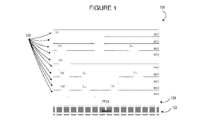
[0048] Figure 1 is a schematic diagram of a cross-section of an
exemplary sample to
be de-layered, in accordance with one embodiment;
7
CA 03125346 2021-06-29
WO 2020/150814
PCT/CA2020/050060
[0049]
Figure 2 is a schematic diagram of an ion beam milling and monitoring
system, in accordance with one embodiment;
[0050]
Figures 3A and 3B are schematic diagrams illustrating exemplary changes in a
measured current as monitored by the system of Figure 2, in the case of BIB
and FIB
milling, respectively and in accordance with different embodiments;
[0051]
Figure 4 is a flow diagram describing a method of monitoring de-layering of
an unknown sample by a broad ion beam mill, in accordance with one embodiment;
[0052]
Figure 5 is a schematic diagram of an ion beam milling endpoint detection
system, in accordance with one embodiment;
[0053] Figure 6 is a flow diagram describing an ion milling endpoint
detection
method, in accordance with one embodiment; and
[0054]
Figure 7 is a schematic diagram of an ion beam milling endpoint detection and
control system, in accordance with one embodiment.
[0055]
Elements in the several figures are illustrated for simplicity and clarity and
have not necessarily been drawn to scale. For example, the dimensions of some
of the
elements in the figures may be emphasized relative to other elements for
facilitating
understanding of the various presently disclosed embodiments. Also, common,
but well-
understood elements that are useful or necessary in commercially feasible
embodiments
are often not depicted in order to facilitate a less obstructed view of these
various
embodiments of the present disclosure.
DETAILED DESCRIPTION
[0056]
Various implementations and aspects of the specification will be described
with reference to details discussed below. The following description and
drawings are
illustrative of the specification and are not to be construed as limiting the
specification.
Numerous specific details are described to provide a thorough understanding of
various
implementations of the present specification. However, in certain instances,
well-known
8
CA 03125346 2021-06-29
WO 2020/150814
PCT/CA2020/050060
or conventional details are not described in order to provide a concise
discussion of
implementations of the present specification.
[0057]
Various apparatuses and processes will be described below to provide
examples of implementations of the system disclosed herein. No implementation
described below limits any claimed implementation and any claimed
implementations
may cover processes or apparatuses that differ from those described below. The
claimed
implementations are not limited to apparatuses or processes having all of the
features of
any one apparatus or process described below or to features common to multiple
or all of
the apparatuses or processes described below. It is possible that an apparatus
or process
described below is not an implementation of any claimed subject matter.
[0058]
Furthermore, numerous specific details are set forth in order to provide a
thorough understanding of the implementations described herein. However, it
will be
understood by those skilled in the relevant arts that the implementations
described herein
may be practiced without these specific details. In other instances, well-
known methods,
procedures and components have not been described in detail so as not to
obscure the
implementations described herein.
[0059] In
this specification, elements may be described as "configured to" perform
one or more functions or "configured for" such functions. In general, an
element that is
configured to perform or configured for performing a function is enabled to
perform the
function, or is suitable for performing the function, or is adapted to perform
the function,
or is operable to perform the function, or is otherwise capable of performing
the function.
[0060] It
is understood that for the purpose of this specification, language of "at
least
one of X, Y, and Z" and "one or more of X, Y and Z" may be construed as X
only, Y
only, Z only, or any combination of two or more items X, Y, and Z (e.g., XYZ,
XY, YZ,
ZZ, and the like). Similar logic may be applied for two or more items in any
occurrence
of "at least one ..." and "one or more..." language.
[0061]
The systems and methods described herein provide, in accordance with
different embodiments, different examples in which a broad ion beam (BIB) or
focused
9
CA 03125346 2021-06-29
WO 2020/150814
PCT/CA2020/050060
ion beam (FIB) de-layering and monitoring system and method can be used for
monitoring and controlling the delayering of an unknown sample by measuring
changes
in the magnitude of electrical current flowing to or from the sample during
milling. Such
a system may be used as an endpoint monitoring system or unit to better
control the
.. milling parameters, such as but not limited to the milling rate, during the
removal of one
or more layers of the unknown sample.
[0062]
Such a sample may be comprised of a composition of one or more materials.
A sample may also refer to, but is not limited to: a semiconductor device,
Integrated
Circuit, a layer of metals and dielectrics of any thickness, one or more
materials in an
area of any size, optical devices, electronic devices, or any combinations
thereof. A
worker skilled in the art would readily understand the meaning of a sample for
the
purposes of the subject matter disclosed herein. While the present disclosure
describes
various embodiments for illustrative purposes, such description is not
intended to be
limited to such embodiments. On the contrary, the applicant's teachings
described and
illustrated herein encompass various alternatives, modifications, and
equivalents, without
departing from the embodiments, the general scope of which is defined in the
appended
claims. Except to the extent necessary or inherent in the processes
themselves, no
particular order to steps or stages of methods or processes described in this
disclosure is
intended or implied. In many cases the order of process steps may be varied
without
changing the purpose, effect, or import of the methods described.
[0063]
Delayering may entail, but is not limited to: removal of one or more layers,
partly or wholly, wherein the one or more layers or portions thereof may
comprise one or
more materials; removal of one or more layers, partly or wholly, comprising
one or more
materials, wherein the one or more layers may comprise small or large surface
areas;
.. removal of one or more layers, partly or wholly, wherein the one or more
layers may be
of any desired thickness; removal of one or more materials, partly or wholly,
to any
extent desired; removal of one or more substantially parallel layers, partly
or wholly,
wherein the one or more substantially parallel layers or portions thereof may
comprise
one or more materials; removal of one or more substantially planar layers,
partly or
wholly, wherein the one or more substantially planar layers or portions
thereof may
CA 03125346 2021-06-29
WO 2020/150814
PCT/CA2020/050060
comprise one or more materials; removal of one or more substantially constant
thickness
parallel layers, partly or wholly, wherein the one or more substantially
constant thickness
parallel layers or portions thereof may comprise one or more materials;
removal of one or
more varying thickness parallel layers, partly or wholly, wherein the one or
more varying
.. thickness parallel layers or portions thereof may comprise one or more
materials or any
combinations thereof. For the purposes of the subject matter disclosed herein,
the terms
delayering and de-layering may be used interchangeably. Delayering may be set
to take
place for a certain time; after which, the sample may be removed from the ion
beam mill,
analyzed, and further delayering necessitated, until the desired level of
delayering is
1() achieved
[0064] In
the case of an IC sample, delayering may be performed for reverse
engineering the circuitry inherent within a device. An ion beam mill may be
used to
delayer a device layer by layer and exposing the circuitry or circuit
connections on the
surface of each layer. Upon delayering the device, pictures, images or other
representation (e.g. circuit schematic model based on data representative of
detected
surface features) may be taken of each layer, thereby, capturing the circuitry
or circuit
connections on the surface of each layer. By piecing together, the pictures,
images, or
other representations of the different layers, using appropriate software
tools, circuit
connections between the various components that may be inherent within a
device, both
across and between layers, can be produced. The process may be repeated for
various
devices within a larger device and a hierarchical schematic of the circuit
connections of
the various devices within the larger device may be developed. Proprietary
software tools
may also be used to produce hierarchical circuit schematics. Such circuit
schematics may
be useful in identifying evidence of use of claim elements in the target
device being
delayered. According to some embodiments, delayering may be performed for, but
is not
limited to, failure analysis (defect identification), circuit edit,
sample/device
characteristics measurement, verification of design, and counterfeit
detection.
[0065]
With reference to Figure 1, and in accordance with one exemplary
embodiment, a schematic diagram of a cross-section of an exemplary sample to
be de-
layered, generally referred to using the numeral 100, will now be described.
In this
11
CA 03125346 2021-06-29
WO 2020/150814
PCT/CA2020/050060
exemplary embodiment, the sample is an integrated circuit (IC). In general, an
IC may
take the form of a multi-wiring layer structure, in which a wiring layer and
an insulating
layer are laminated. Each layer or portions thereof may be made up of one or
more
materials, or a mixture of materials such as, but not limited to, metal
interconnects and
dielectrics in varying shapes and structures. For example, in Figure 1 the
bottommost
layer (i.e. substrate) 102 may be mostly comprised of a silicon layer. Above
this layer is
the Front-end-of-line (FEOL) region 104 comprising a multiplicity of
transistors built
directly on the silicon. Above this there is a number of interconnection
layers 105,
comprising different amounts of metal interconnects and dielectric materials
(such as a
spin-on dielectric (SOD) or chemical vapor deposited (CVD) dielectric), each
separated
for example by a thin layer of SO2 or silicon oxycarbide. A worker skilled in
the art
would readily understand the layers within an IC and how each layer may be
characterized by the presence and quantity of different types of materials,
such as, but not
limited to those mentioned above.
[0066] When an ion beam of positively charged ions impinges on the exposed
surface
of such a sample, the high energy primary ions collide with the solid surface,
transferring
energy from the primary particle to the atoms of the material to be milled.
Some of the
primary ions can be back scattered but most of them transfer their kinetic
energy to the
lattice through a collision sequence and are implemented into the target
according to their
energy, mass and impact angle. Ions that impact the exposed material with
sufficient
energy will dislodge atoms or molecules and generate the emission of secondary
electrons and photons. Ion milling is an etching process where the ion beam is
used so
that the material in the exposed surface of the sample is to be etched away.
The
implementation of the primary ions, followed by the generation of secondary
ions and
ejected electrons may lead to the increase or build-up of positive charges in
the sample's
surface. Depending on the conductivity of the material being irradiated, these
charges
may be more or less mobile. When such a sample is being de-layered with an ion
beam,
the layers are slowly exposed sequentially from the top surface. The exposed
surface of
the sample may be non-homogenous (i.e. heterogeneous) and therefore constitute
different compositions of materials or it may also be homogenous, which
constitutes a
single material composition. Upon delayering a surface of a sample, the
underlying
12
CA 03125346 2021-06-29
WO 2020/150814
PCT/CA2020/050060
surface may be left substantially uniform or even regardless of the delayered
surface
being homogenous or non-homogenous. Upon delayering a surface of a sample, the
underlying surface may also be left substantially non-uniform or uneven. With
reference
to Figure 2, and in accordance with one exemplary embodiment, a schematic
diagram of
an ion beam milling and monitoring system, generally referred to using the
numeral 200,
will now be described. In this exemplary embodiment, the system 200 is used in
the
context of a sample 202 being impinged by a broad ion beam 204 generated by an
ion
beam mill 206. Ion beam 206 may be a broad ion beam (BIB) mill, a focused ion
beam
(FIB), a plasma FIB, or other ion beam technologies, as may be readily
appreciated by
the skilled artisan. Such an ion beam mill is generally configured by
adjusting one or
more of its operating characteristics. The one or more ion beam mill operating
characteristics may be associated with a predetermined rate at which a
material may be
removed. Delayering a sample may be achieved by configuring the ion mill to
remove
one or more materials from the sample at their respective predetermined rates.
The
association of rates of removal to sets of ion mill operating characteristics
may be
obtained experimentally through trial and error or via simulation methods. The
rates of
removal and their associated sets of ion mill operating characteristics may be
logged or
stored for future manipulation of the ion mill in any storage medium such as a
database,
memory device, computing storage device or any storage medium as would be
known to
a worker skilled in the art. The ion beam mill 206 may also consist of one or
more ion
beam sources. For example, ion mill 206 may comprise one or more large
diameter
gridded ion beam source, such as an argon source, but other ion sources, such
as
elemental gold, gallium, iridium, xenon, as well any other suitable ion
sources, may also
be used. Moreover, various gas injection systems may deliver different process
gasses
during milling, while a plasma bridge neutralizer may be used to neutralize
the ion beam.
Vacuum gauges, a load-lock, vacuum pumps, one or more control panels, and one
or
more processors may also be associated with the ion mill. Furthermore, one or
more ion
beam sources may be associated with apertures and electrostatic lenses. It is
to be
understood that the operation of an ion mill and the various fundamental
components of
an ion mill would be readily known to a worker skilled in the art. The sample
202 may be
mounted on a, variable angle, cooled sample stage 208 that can be tilted and
rotated. As
13
CA 03125346 2021-06-29
WO 2020/150814
PCT/CA2020/050060
mentioned above, such a sample stage may be housed in a vacuum chamber. The
skilled
worker in the art will readily understand how a sample is affixed to such a
rotating stage,
including the different methods of insuring a good thermal and electrical
contact.
[0067]
The monitoring system 200 itself comprises an electrical conductor (e.g. an
.. electrical wire) 210 connecting sample 202 to ground 212 in such a way that
allows for
any freely moving charges to flow from sample 202 as it is being irradiated or
milled. A
current measuring device 214, such as an analogue or digital ammeter or
similar may be
connected to conductor 210 between sample 202 and ground 212 to measure this
current
(stage current, sample current, absorbed current, etc.) and the changes
thereto. In some
.. embodiments, an optional biasing voltage 218 may also be added to increase
or improve
the current detected in current measuring device 214, depending on polarity of
ions used
and/or other operational considerations, as will be readily understood by the
skilled
technician. The falling or rising trend in the current thus measured will be,
as explained
below, indicative of a change in the nature of the layer currently being
milled. These
.. trends may be used to monitor the milling process itself, and/or to provide
the means to
the ion beam operator to measure when an endpoint is reached. In some
embodiments,
conductor 210 may be connected to a bottom region of sample 202. The skilled
artisan
will understand that many techniques may be employed to reliably connect
sample 202 to
an electrical conductor 210. In other embodiments, the electrical conductor
210 may
instead be connected to stage 208 if both sample 202 and stage 208 already
have a good
electrical connection, for instance by using a thin layer of electrically
conductive vacuum
grease or similar. Alternatively, if the current flowing from sample 202
during irradiation
is too small to be accurately measured, a current amplifying device 216 such
as a pre-
amplifier or similar may also be connected to conductor 210 between sample 202
and the
.. current measuring device 214.
[0068]
With reference to Figures 3A and 3B, and in accordance with different
exemplary embodiments, schematic diagrams illustrating the changes in the
measured
current as monitored by the system of Figure 2, generally referred to using
the numeral
300, will now be described. As explained above, de-layering this type of
structure will
expose sequential surface areas with larger amounts of conductive material
(wiring layer)
14
CA 03125346 2021-06-29
WO 2020/150814
PCT/CA2020/050060
followed by areas with larger amounts of dielectric material (insulating
layer). If such a
sample was to be electrically connected to ground, accumulated charges
produced by the
ion beam in the sample would cause a current to flow therefrom. However, the
magnitude
of such a current would be dependent on the type of material being irradiated.
For
instance, the high conductivity of a metallic material (pure metal or metallic
alloy) would
tend to produce a higher current, while the low conductivity of a dielectric
material (i.e.
silicon dioxide, silicon nitride, etc.) would restrict the free flow of
charges. Thus, a direct
measurement of the current flowing from the sample during ion milling will
show
changes or variations such as a rising or falling trend as the sample is de-
layered.
[0069] In both cases where a BIB or FIB mill is used (or other ion beam
technologies
that may typically exhibit broader or narrower beam spot sizes), the current
from the
sample is measured from the moment the mill is activated, at which point the
current is
expected to rise rapidly. Therefrom, the measured current is expected to
change
depending on the type of material being milled (in contact with the ion beam).
Layers
composed primarily of highly conductive materials (such as metals), when hit
by the
positive ions, are expected to produce a higher current, while a reduced
current is
expected when the layer is primarily composed of electrically isolating
materials. Figure
3A shows a schematic plot of the measured current as a function of milling
time (e.g.
milling depth) when using a BIB mill. Such mills have beams that are typically
broad
enough to cover the entire surface of interest of the sample at the same time,
therefore the
measured current will be a sum of all the interactions with all the features
(metal
interconnects and/or dielectric) of the surface at a given time. Therefore,
while some
variation is expected in the shape or profile of the measured current for a
given layer,
constituent materials, or material compositions, as discussed above, generic
features or
trends are nonetheless to be expected and may thus be used or relied upon, at
least in part,
to differentiate between layers, and constituent materials or material
compositions
thereof. As seen in Figure 3A, for example, each time a surface layer
comprising metal
interconnect-rich regions is milled, a higher current is measured, producing
"peaks"
and/or "plateaus" (304), while milling dielectric-rich regions will tend to
produce
significantly lower electric currents (306). Finally, once all the functional
layers are
CA 03125346 2021-06-29
WO 2020/150814
PCT/CA2020/050060
milled and the beam reaches the bottom substrate layer, an intermediary and
constant
current should be measured.
[0070]
Thus, the alternating layers within the sample will produce an alternating
current signature. This alternating change in the measured current may then be
readily
used to identify the type of material (e.g. metallic vs insulating) and thus
characterize the
layer currently being milled. The exact amplitude of these peaks and valleys
may vary
depending on the details of the implementation and depending on the exact
nature and
quantity of material being milled at each layer. Thus, the exact current
profile from layer
to layer may deviate from the one of Figure 3A and the change in current may
not only
take the form of shallow or broad peaks, but it may also take the form of an
inflection
point. However, the characteristic relative "rising and falling" variation
between a higher
current and a lower current measured as sequential layers are being milled is
expected to
remain for most types of samples, thus generally allowing for the visual
and/or automated
inspection and identification of layer boundaries/transitions during milling,
and/or the
establishment of current flow threshold or trend changes indicative of such
boundaries/transitions. In addition, two or more regions of low current (high
current) may
also be compared to identify the presence of two or more insulating materials
(metallic
materials). As such, two generally low (high) current regions may both contain
a
substantial amount of dielectric (conductive) material, but the difference
between the
absolute measured current in each region may also provide the means to
differentiate
between each insulating (metallic) material. By identifying the general
composition of
the exposed surface layer, it may be possible to characterize the layer itself
with respect
to functional features present therefrom. This characterization may be used to
identify the
layer, for example to identify if the layer is a pre-determined endpoint layer
where the
milling process is to be stopped.
[0071] In
contrast, Figure 3B illustrates schematically the measured stage current
obtained when using a FIB mill or similar. FIB milling involves raster
scanning the
focused ion beam across a sample surface and a whole layer is removed only
when a full
scan of the surface is completed. Thus, monitoring a FIB milling process may
require not
only measuring the stage current (which may be smaller as the ion beam covers
less
16
CA 03125346 2021-06-29
WO 2020/150814
PCT/CA2020/050060
material compared to a BIB mill) as a function of time (or milling time) but
also keeping
track of successive scan cycles. The stage current will therefore vary a great
deal within a
given scan cycle, as the FIB mills smaller portions of the sample surface,
hitting metallic
and/or dielectric materials. However, it is the relative difference between
regions of
measured current indicative of successive scan cycles that can be used to
determine a
transition between layers. Figure 3B gives an exemplary plot of such a
measurement,
wherein three successive scan cycles are illustrated (N, N+1 and N+2). The
first two
cycles comprise a relatively high portion of higher measured currents,
indicative that
associated milled layers comprised a relatively high portion of metal
interconnects. In
contrast, cycle N+2 shows a markedly lower number of higher current
peaks/plateaus,
indicative that the present layer being milled is located at or near a
transition region
located at a depth between two metal interconnect rich layers. In some FIB
embodiments,
additional signal analysis techniques, in real-time or near real-time, such as
integrating
the measured current during a full scan cycle and/or applying a running
average or
similar, may be used to improve the detection of successive surface layers.
[0072]
Naturally, various ion beam parameters may impact the measured current
profile and approach to differentiating between conductor-rich and dielectric-
rich layers.
For instance, the BIB example represents one end of the spectrum where the ion
beam
spot size is typically equal or greater than an entire surface of the sample
being milled,
resulting in a measured current that automatically averages over all surface
features. As
illustrated above, a particularly narrow beam implementation, such as in a FIB
implementation, will result in a more variable current profile as the beam
sequentially
interacts with different portions of the sample's exposed surface.
Accordingly,
parameters such as scan/raster speeds, spot size relative to surface features,
accumulated
charge detection speeds may impact a general surface resolution or feature
specificity of
the acquired measured current profiles, and thus impact how such signals can
be averaged
and/or otherwise combined to provide layer or surface level information useful
in
distinguishing distinctly composed sample layers.
[0073]
With reference to Figure 4, and in accordance with one exemplary
embodiment, a flow diagram describing a method of monitoring the de-layering
of an
17
CA 03125346 2021-06-29
WO 2020/150814
PCT/CA2020/050060
unknown sample by a broad ion beam mill, generally referred to using numeral
400, is
explained. First (402), prior to activating the ion beam mill, the sample to
be de-layered,
once installed on the stage is connected, using an electrical conductor (e.g.,
wire or
similar), to ground. Once the milling process is started by initiating the
mill, the current
flowing from the sample to ground is measured (408) using as mentioned above
an
electrical current measuring device such as an ammeter. As explained above,
the current
measured is expected to vary when milling consecutive layers of the sample. In
the case
of a BIB mill, the measured current amplitude is directly expected to be
indicative of the
composition of all material types contained within the layer, while for a FIB
mill, the
current amplitude measured during an entire scan cycle may be used instead.
These
changes may be used to identify the constituent materials or type of materials
on the
exposed surface of the milled layer (412). From this information, it may be
possible to
characterize the exposed layer being irradiated (416) with respect to previous
layers and
determine therefrom if this layer is an endpoint layer. If it is the case, the
skilled
technician will be able to respond by changing one or more ion mill operating
characteristics or parameters, for example to adjust the material removal
rate, or he may
stop the milling process altogether if this is what is desired. As noted in
the below
examples, such operational decisions may also or otherwise be automated by
establishing
designated endpoint detection thresholds or like values to be assessed by a
digital data
processor operatively associated with the current measuring device and ion
beam mill.
[0074]
With reference to Figure 5, and in accordance with one exemplary
embodiment, a schematic diagram of a ion beam milling endpoint detection
system,
generally referred to using the numeral 500, will now be described. The system
500 is
similar to the one described above with reference to Figure 2, in that it also
comprises an
electrical conductor (e.g. an electrical wire, etc.) 510 connected from sample
502 to
ground 512 in such a way that allows for any freely moving charges to flow
from a
sample 502 as it is being de-layered with an ion beam 504 generated by a
(broad or
focused) ion beam mill 506. Similarly, system 500 again comprises a current
measuring
device 514, such a digital ammeter or similar, which may again be connected to
conductor 510 between sample 502 and ground 512 to measure this current (stage
current, sample current, absorbed current, etc.) and the changes thereto. In
some
18
CA 03125346 2021-06-29
WO 2020/150814
PCT/CA2020/050060
embodiments, an optional biasing voltage 522 may also be added to increase or
improve
the current measured in current measuring device 514, depending on polarity of
ions used
and/or other operational considerations, as will be known to the skilled
technician. In
addition, system 500 further comprises a digital data processor 518
operatively connected
to the current measuring device 514, for example via a digital interface, and
operable to
automatically identify, in real-time or near real-time, from the changes in
the measured
current, the presence and quantity of different types of constituent materials
and further
operable to characterize, from said type of materials, the layer currently
being milled. For
example, such changes, boundaries and/or transitions may be preprogrammed to
1()
correspond with certain designated current increase/decrease thresholds,
values and/or
ranges, which may be determined from prior testing, sampling and/or
observations using
the system 500 and similar samples, or again, incrementally learned by the
system or
operator thereof based on current variation trends, profiles or the like. It
will be
appreciated that the processor 518 may take various forms, which may include,
but is not
limited to, a dedicated computing or digital processing device, a general
computing
device or other computing device as may be readily appreciated by the skilled
artisan. In
some embodiments, processor 518 may be operationally connected to a digital
display
interface 520, which may comprise a computer with a digital display screen,
tablet,
smartphone application or like general computing device, or again a dedicated
device
having a graphical or like general computing device. Finally, as described
above, system
500 may comprise a current amplifying device 516 such as a pre-amplifier or
similar,
connected to conductor 510 between sample 502 and the current measuring device
514
and operable to increase the current flowing thereto.
[0075]
With reference to Figure 6, and in accordance with one exemplary
embodiment, a flow diagram describing a method of ion beam milling endpoint
detection
and control, generally referred to using the numeral 600, for the de-layering
of an
unknown sample by a broad ion beam mill, will now be described. This exemplary
embodiment is similar to the one described above with reference to Figure 4,
in that it
also comprises the steps of first connecting the sample to ground (602), but
further
includes the steps related to the control of the ion beam mill itself. This
includes first
activating the (broad or focused) ion beam (604) before proceeding with, as
before,
19
CA 03125346 2021-06-29
WO 2020/150814
PCT/CA2020/050060
continuously measuring (606) the current flowing from the sample and
identifying from
changes therefrom the type of material present within the exposed layer (608)
and
characterizing therefrom the layer being milled (610). In addition, the
present method
includes the step of determining from said characterization if the current
layer being
milled has been pre-determined to be an endpoint layer (612). If this is not
the case (e.g.
transitioning to or within a dielectric layer in an integrated circuit where
current flow is
relatively lower), then the current is again continuously monitored (602). In
the case
where the layer is an endpoint layer (e.g. transitioning to or within a
circuit layer in an
integrated circuit where current flow is relatively higher), then the ion beam
is turned off
1() to
stop the milling process (614). In some embodiments, it may be desirable to
change the
milling rate instead of stopping the milling process altogether, depending on
the
application at hand.
[0076]
With reference to Figure 7, and in accordance with yet another exemplary
embodiment, a schematic diagram of an ion beam milling endpoint detection and
control
system, generally referred to using the numeral 700, will now be described.
The system
700 is similar to the one described above with reference to Figure 5, in that
it also
comprises an electrical conductor (e.g. an electrical wire, etc.) 710
connected from
sample 702 to ground 712 in such a way that allows for any freely moving
charges to
flow from a sample 702 as it is being de-layered with a broad ion beam 704
generated by
a broad or focused ion beam mill 706. Similarly, system 700 again comprises a
current
measuring device 714, such as a digital ammeter or similar that is again
connected to
conductor 710 between sample 702 and ground 712 to measure this current (stage
current, sample current, absorbed current, etc.) and the changes thereto. In
some
embodiments, an optional biasing voltage 724 may also be added to increase or
improve
the current flowing in current measuring device 714, depending on polarity of
ions used
and/or other operational considerations, as will be known to the skilled
technician. The
system further comprises a digital data processor 718 operatively connected to
the current
measuring device 714, for example via a digital interface, and operable to
automatically
identify, in real-time or near real-time, from the changes in the measured
current, the
presence and quantity of different types of materials, and further operable to
characterize,
from said type of materials, the layer currently being milled and determine if
it
CA 03125346 2021-06-29
WO 2020/150814
PCT/CA2020/050060
corresponds to a pre-determined endpoint. The currently described exemplary
embodiment further comprises the BIB mill 706 and sample stage 708 themselves,
in
addition to a controller 720 operatively connected to said digital processor
718 (which
may be integral thereto or operatively associated therewith), mill 706, and
stage 708, and
operable to provide endpoint control to the milling process by changing one or
more ion
mill operating characteristics or parameters, for example to adjust the
material removal
rate, and/or stopping the milling process altogether when an endpoint layer is
reached.
The artisan well versed in the art of BIB milling will be familiar with the
different control
parameters that may be used therefor.
[0077] Information as herein shown and described in detail is fully capable
of
attaining the above-described object of the present disclosure, the presently
preferred
embodiment of the present disclosure, and is, thus, representative of the
subject matter
which is broadly contemplated by the present disclosure. The scope of the
present
disclosure fully encompasses other embodiments which may become apparent to
those
skilled in the art, and is to be limited, accordingly, by nothing other than
the appended
claims, wherein any reference to an element being made in the singular is not
intended
to mean "one and only one" unless explicitly so stated, but rather "one or
more." All
structural and functional equivalents to the elements of the above-described
preferred
embodiment and additional embodiments as regarded by those of ordinary skill
in the art
are hereby expressly incorporated by reference and are intended to be
encompassed by
the present claims. Moreover, no requirement exists for a system or method to
address
each and every problem sought to be resolved by the present disclosure, for
such to be
encompassed by the present claims. Furthermore, no element, component, or
method
step in the present disclosure is intended to be dedicated to the public
regardless of
whether the element, component, or method step is explicitly recited in the
claims.
However, that various changes and modifications in form, material, work-piece,
and
fabrication material detail may be made, without departing from the spirit and
scope of the
present disclosure, as set forth in the appended claims, as may be apparent to
those of
ordinary skill in the art, are also encompassed by the disclosure.
21