Note: Descriptions are shown in the official language in which they were submitted.
CA 03125824 2021-07-06
WO 2020/152393 1 PCT/F12020/050012
JOSEPHSON TRAVELING WAVE PARAMETRIC AMPLIFIER
FIELD
[0001] The present invention relates to superconducting traveling wave
parametric
amplifiers, TWPAs.
BACKGROUND
[0002] Parametric amplifiers are in effect mixers, wherein a weaker
input signal may
be amplified by mixing it with stronger pump signal, producing a stronger
output signal as
.. a result. Parametric amplifiers rely on a nonlinear response of a physical
system to
generate amplification. Such amplifiers may comprise standing wave parametric
amplifiers
or traveling wave parametric amplifiers, wherein a traveling wave parametric
amplifier
uses a series of nonlinear elements distributed along a transmission line,
such as a coplanar
waveguide, for example. In case the nonlinear elements comprise Josephson
junctions, the
.. amplifier may be referred to as a Josephson traveling wave parametric
amplifier, JTWPA.
In a JTWPA, the Josephson junctions are maintained in superconducting
condition and
carry a supercurrent.
[0003] In use, a signal is added to the strong oscillator signal,
resulting in a sum
signal wherein an amplitude envelope exhibits variance at a frequency which is
a
.. difference between the signal and oscillator frequencies. Since in the
waveguide
transmission line, a phase velocity is dependent on amplitude, a phase of the
summed
signal at the end of the line will vary in accordance with a difference in the
two
frequencies. In effect, the nonlinear waveguide transmission line converts
amplitude
modulation into phase modulation. In case the non-linearity is strong enough,
this will
result in a gain at the signal frequency.
2
SUMMARY OF THE INVENTION
[0004] According to some aspects of the invention, there is provided
the subject-
matter described herein.
[0005] According to a first aspect of the present invention, there is
provided a
travelling wave parametric amplifier comprising a waveguide transmission line
comprising
therein at least ten Josephson elements, wherein each of the at least ten
Josephson element
comprises a loop, with exactly one Josephson junction of first size on one
half of the loop
and at least two Josephson junctions of a second size on a second half of the
loop, the
second size being larger than the first size, a flux bias line configured to
generate a
magnetic flux threading each of the at least one loop, and a set of resistors
coupled with the
flux bias line.
[0006] According to a second aspect of the present invention, there
is provided a
method for manufacturing a traveling wave parametric amplifier comprising
providing a
waveguide transmission line comprising therein at least ten Josephson
elements, wherein
each of the at least ten Josephson elements comprises a loop, with exactly one
junction of
first size on one half of the loop and at least two junctions of a second size
on a second half
of the loop, the second size being larger than the first size, providing a
flux bias line
configured to generate a magnetic field threading each of the at least one
loop, and
providing a set of resistors coupled with the flux bias line.
BRIEF DESCRIPTION OF THE DRAWINGS
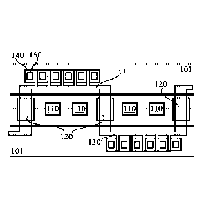
[0007] FIGURE 1 illustrates an example amplifier in accordance with
at least some
embodiments of the present invention;
[0008] FIGURE 2 illustrates an example Josephson element in accordance with
document [2];
[0009] FIGURE 3 illustrates an example Josephson element in
accordance with at
least some embodiments of the present invention, and
CA 3125824 2022-04-22
CA 03125824 2021-07-06
WO 2020/152393 3 PCT/F12020/050012
[0010] FIGURE 4 is a flow graph of a method in accordance with at least
some
embodiments of the present invention.
EMBODIMENTS
[0011] In accordance with solutions disclosed herein, a traveling wave
parametric
amplifier may be made less sensitive to errors in the size of smaller
Josephson junctions in
a Josephson element comprising larger and smaller Josephson junctions, by
selecting
parameters suitably. Further, a gradiometric layout of a Josephson element is
disclosed,
which renders the element sensitive to a magnetic field gradient only, and a
flux bias line
in the traveling wave parametric amplifier is provided to generate such a
field gradient.
Further, the transmission line may be tapered. Overall, using one of more of
these
enhancements, a traveling wave parametric amplifier may be more suitably used
in real-
life applications as its operation will be less sensitive to disturbances and
manufacturing
defects.
[0012] FIGURE 1 illustrates an example amplifier in accordance with at
least some
embodiments of the present invention. Overall, for example in quantum
computation,
signals may be attenuated for transmission even to a single-photon or a near-
single-photon
regime. Detecting such signals presents challenges owing to their low
amplitude.
Therefore, suitable amplifiers may be employed to increase the amplitudes of
received
signals prior to their provision to detector elements, where the information
encoded into
these received signals may be recovered. As another example, a single-photon
regime
communication may be employed in communicating encryption keys in a secure
manner
using quantum communication, such that eavesdropping without detection is made
very
difficult.
[0013] The present disclosure is focuses on a superconductive
realization of the
TWPA, where the center trace of a transmission line is an array of Josephson
junction
based elements, known as Josephson elements, that constitute a non-linear
inductance. The
non-linearity allows for a mixing process that provides power gain for a weak
signal that
propagates along the same direction as a strong radio frequency, rf, pump
tone. The
strength of the pump tone is measured with the ratio between the pump current
amplitude
CA 03125824 2021-07-06
WO 2020/152393 4 PCT/F12020/050012
1p and the critical current Ic of the Josephson element. The nature of the non-
linearity
depends on the arrangement of Josephson junctions within the element. The
simplest
realization is the use of a single Josephson junction as the non-linear
element: the
associated Taylor expansion of the inductance is a constant plus a term
proportional to
(Ip/Ic)^2, that is, a Kerr non-linearity. While the Kerr term results in a
desired mixing
process, it also changes the wavevector of the pump tone, an effect that has
to be
compensated with dispersion engineering. The balancing of the wavevectors,
also called
phase matching, allows an exponential increase of the TWPA gain as a function
of the
device length. Due to the typically narrowband dispersive features embedded
into the
transmission line, the center frequency of gain is a fixed quantity in this
example of the
TWPA.
[0014] There are new solutions that target the realization of a Kerr-
free non-linearity
by introducing a magnetic flux degree of freedom to the Josephson element. In
the Taylor
expansion of the inductance, this alternative non-linearity is a term
proportional to Ip/Ic.
Kerr-free operation is beneficial as no dispersion engineering is necessary to
achieve phase
matching. The pump frequency, which sets the center frequency of gain, can be
freely
selected. Main features of a typical Kerr-free element include (i) a
superconductive
magnetic pick-up loop that can be pictured as two half-loops connected
together, (ii) the
interruption of the two halves with an unequal number of Josephson junctions,
and (iii) a
finite magnetic flux bias that makes a screening current flow in the loop
according to the
principle of flux quantization. Particular weaknesses of the Kerr-free
element, in the
realizations presented so far, are (i) sensitivity to magnetic interference,
and (ii) sensitivity
to inhomogeneity of the magnetic bias field, especially in arrays consisting
of multiple
elements.
[0015] Furthermore, a generic problem in TWPAs is depletion of the pump
current.
This is due to either dissipation in the transmission line, or transfer of
power from the
pump to the amplified signal if the TWPA is operated close to saturation. The
pump
depletion limits the TWPA gain because the mixing process relies on a suitable
ratio
between Ip and lc. Another generic problem in TWPAs is the fabrication spread
of the Ic,
causing inhomogeneity of the electrical parameters of the transmission line.
[0016] The JTWPA of FIGURE 1 comprises a waveguide, which comprises
Josephson elements 110 and parallel-plate capacitors 120. The Josephson
elements 110 are
CA 03125824 2021-07-06
WO 2020/152393 5 PCT/F12020/050012
connected with each other with waveguides capable of conveying electromagnetic
waves,
as is known in the art. The waveguide, a section of which is illustrated in
FIGURE 1, has
an input port at the left, arranged to receive the signal to be amplified and
a strong
oscillator signal, which are mixed in the waveguide in the non-linear
Josephson elements
110. At an output port at the right, the phase-modulated amplified signal is
obtained as
output. Two wiring layer elements 101 may each comprise a superconductor
covered with
an insulator, for example.
[0017] In general, a Josephson element, such as a single junction, a
superconducting
quantum interference device (SQUID), an asymmetric SQUID, or a more complex
.. Josephson element such as a flux-qubit-like circuit, can be described using
an effective
potential energy:
[0018] Ueff{(p)/Ej = c2cp2 + C3(P3 + C4(P4 +
[0019] here Ej is the Josephson energy, and qi is the superconducting
phase. The c2
term relates to critical current and linear part of Josephson inductance, the
cl term relates to
.. 3-wave mixing and the c4 term relates to 4-wave mixing, which is also known
as the Kerr
nonlinearity.
[0020] Normally single junctions and SQUIDs, including asymmetric
SQUIDs, have
c3 = 0, whereby 3-wave mixing does not occur, and non-linearity is provided by
the Kerr
term. 3-wave mixing means the ability to pump at twice the input frequency,
which is
desirable. 3-wave mixing could be activated by injecting a dc current, but
however, the
Kerr term would remain non-zero.
[0021] Nonlinearity provided by the Kerr term is associated with the
need for
resonant phase matching, in practice the pump signal is given a small phase
increment at
regular intervals along the transmission line. This is due to the pump having
a different
phase velocity from the signal (at the frequency fP) and the idler (at the
frequency fl). This
phase mismatch increases with the pump power. Conservation of energy implies
the
existence of an idler frequency at the output, the frequency of which is
located at the
"mirror image" of the signal frequency with respect to the pump, fl=2fP¨fS. In
detail, in
the Kerr mode, phase mismatch and gain depend on the same parameter, the Kerr
nonlinearity. The three frequencies are related by fS+fl=fP in the case of 3-
wave mixing.
CA 03125824 2021-07-06
WO 2020/152393 6 PCT/F12020/050012
To minimize the amount of reflections, both ends of the TWPA further need to
have good
impedance match at each of the frequencies fl, fS and fP.
[0022] Consequently, it would be preferable to operate a TWPA using 3-
wave
mixing without 4-wave mixing, that is, using the c3-term with the Kerr
nonlinearity
suppressed. Thus the amplifier could be constructed without equipment for
providing the
periodic phase increments which are necessitated by the Kerr mode. In the 3-
wave mode,
phase mismatch and gain depend on different nonlinear terms.
[0023] In particular, the present invention sets out to solve, or at
least alleviate, the
following problems: firstly, sensitivity to magnetic interference in a Kerr-
free TWPA. The
interference may compromise the ultralow-noise performance of the TWPA.
Secondly,
sensitivity to inhomogeneity of the magnetic bias field in the Kerr-free TWPA.
Thirdly,
fabrication spread of the Josephson junctions affects the critical current in
the TWPA.
These effects cause variation of the transmission line impedance, a potential
source of
reflections. The reflections can cause standing waves that introduce
periodicity into the
frequency response of the TWPA, or even prevent the mixing process from
providing gain.
Fourthly, depletion of pump current in the TWPA. This limits the maximum gain
of the
TWPA.
[0024] A. B. Zorin describes in [1] a solution, wherein the balance
between c3 and c4
mixing can be controlled by applying a suitable external magnetic field to rf-
SQUIDs.
Thus predominantly 3-wave mixing may be attained in Zorin's system.
[0025] Frattini et al. describe in [2] a flux-qubit-like circuit which
simultaneously
nulls the Kerr mixing term and maximizes the 3-wave mixing term. This circuit,
which the
authors of document [2] name "Superconducting Nonlinear Asymmetric Inductive
eLement", SNAIL, is modified as described herein to arrive at the Josephson
element 110
in the present embodiments. In detail, in [2], a Josephson element has three
large
Josephson junctions on one half of a loop and one small Josephson junction on
the other
half of the loop. In the present solution, a Josephson element with at least
two large
Josephson junctions on one half of a loop and one small Josephson junction on
the other
half of the loop is used. This will be illustrated later in FIGUREs 2 and 3.
[0026] The JTWPA of FIGURE 1 has, in the waveguide, parallel-plate
capacitors
120, interspersed between the Josephson elements 110. Two Josephson elements
110
CA 03125824 2021-07-06
WO 2020/152393 7 PCT/F12020/050012
between every two parallel plate capacitors 120 is one example, to which the
invention is
not limited, indeed, in various embodiments there may be three or more
Josephson
elements 110 between every two parallel plate capacitors 120. The parallel
plate capacitors
120 form the majority of the shunt capacitance of the transmission line. The
JTWPA of
FIGURE 1 is a coplanar waveguide.
[0027] The JTWPA of FIGURE 1 is further furnished with a flux bias
line, FBL,
130. Flux bias line 130 is a two-port circuit that takes a serpentine path,
ranging from one
side of the coplanar waveguide to the other. The flux bias line 130 forms an
upper
electrode of the parallel-plate capacitors 120 in places where it crosses over
to another side
.. of the waveguide, as illustrated in FIGURE 1. The flux bias line 130
connects to the
ground planes of the transmission line through resistors 140, the value of
which is much
smaller than the reactive impedance of the capacitors 120, at the relevant
frequencies fl, fS
and fP. The purpose of the resistors 140 is to provide an rf path to ground
from the
parallel-plate capacitors 120. At the same time, the resistors 140 and the
flux bias line 130
.. enforce a similar electric potential of the ground planes at the
frequencies fl, IS, and fF'.
[0028] As illustrated, flux bias line 130 extends on one side of the
waveguide,
parallel to the waveguide, before ranging over to another side of the
waveguide at a place
corresponding to one of the parallel-plate capacitors 120, to again extend
parallel to the
waveguide on said another side of the waveguide. Where flux bias line 130
extends
parallel to the waveguide, it may be connected, as illustrated, with the
resistors 140, each
of which may form a loop surrounding a contact hole 150. Resistors 140
comprise metal
layers in the present multi-layer JTWPA. Resistors 140 partly overlay the
superconducting
material to form a contact, wherein the resistive aspect of resistors 140 is
generated where
the resistors 140 overlay an insulator, and not the superconductor.
[0029] Operating parameters of the Josephson elements 110 include that
these
elements have at least two large Josephson junctions on one half of a loop and
one small
Josephson junction on the other half of the loop is used. In particular, there
may be two and
only two large Josephson junctions on one half of a loop and one and only one
small
Josephson junction on the other half of the loop. Further, the critical
current of the small
junction is smaller than the critical current of the larger junctions by a
factor of alpha. In
the present Josephson elements 110, alpha may be 0,27. Further, the magnetic
flux
threading through the loops of elements 110 may in the present solution be
0,40 times the
CA 03125824 2021-07-06
WO 2020/152393 8 PCT/F12020/050012
magnetic flux quantum. Thus one parameter combination could be two large
Josephson
junctions and one smaller one, their relation being 0,27 and the magnetic
field amounting
to 0,40 times the flux quantum.
[0030] Dissipation of the resistors adds to the dielectric loss of
parallel-plate
capacitors 120. A dc current in the flux bias line 130 generates the magnetic
field gradient
for the Josephson elements 110. The resistors 140 prevent the leakage of this
current to the
ground plane, and they also prevent the formation of superconductive loops
from the
ground planes and cross-overs. Such superconductive loops could cause the
magnetic flux
to quantize. A current source floating with respect to the waveguide ground
may be
provided for generating the dc current in flux bias line 130.
[0031] The amount of dissipation in the transmission line can be
expressed through
an effective loss tangent of the parallel-plate capacitors 120. Both the pump
current and the
pump voltage experience an exponential decay due to the dissipation when the
characteristic impedance is constant along the transmission line. It would be
desirable if a
fixed ratio were maintained between Ip and Ic to ensure that the mixing
process remains
strong in spite of the dissipation. To this end, either position dependent
capacitance or
position dependent critical current may be applied. , The expression for a
position-
dependent shunt capacitance, that mainly consists of the parallel-plate
capacitors 120, is
derivedbelow. . The capacitance variation maintains a fixed pump current
magnitude along
the transmission line, at the expense of a faster decay of the pump voltage
magnitude.
From the input to the output to the TWPA, the shunt capacitance 120 will
increase. The
characteristic impedance will decrease accordingly, and an impedance-matching
device
may be employed at the output of the device. Examples of an impedance-matching
devices
are a Klopfenstein taper and exponential taper
[0032] In the following, the following notations are employed:
a: unit cell physical length
G: shunt conductance of the unit cell
V: voltage
C: unit cell capacitance
Co: line capacitance at the input, i.e., at x=0
CA 03125824 2021-07-06
WO 2020/152393 9 PCT/F12020/050012
tan 6: loss tangent of C
03: angular frequency
L: unit cell inductance
x: physical coordinate
Z: characteristic impedance
[0033] The power dissipated within an unit cell
reads
Rep/GI/1/2, and the total dissipation from the TWPA input until the position x
is an
integral:
[0034] cxcivi2
j Ca.
0 2a
[0035] We write V = Z1 where the current magnitude I is assumed to be
constant,
and Z = VL/C. Further inserting G = omega*C*tan 6,
[0036] fo
x wc(tanS)Z21/12 dx' = xcoL(tanS)1/12
2a 2a
[0037] Importantly, this dissipation does not change with the possible
variation of C.
On the other hand, we consider the power delivered to position x, that is,
[0038] ROI*/ Z1/12 = VE1112
2 2 2A/T:
[0039] The self-consistent solution for constant I then presents itself
as
0040] 1 _ 1 xcojtanS
[
¨ õTo a =
[0041] Technical effects enabled by the present embodiments include
eliminating a
magnetic shield for superconductive circuits, which typically comprises a
combination of
high-permeability and superconductive layers. The gradiometric design of the
Josephson
element relaxes the magnetic shielding requirement of the Kerr-free TWPA,
allowing
savings in the system cost and size. The gradiometric layout of the Kerr-free
Josephson
element makes the element sensitive to a magnetic field gradient only, as
opposed to also
being responsive to the magnitude of the magnetic field. Furthermore, the
ability to keep
the ratio between the pump current and critical current at a fixed value
enables higher gain
CA 03125824 2021-07-06
WO 2020/152393 10 PCT/F12020/050012
of the TWPA. Parameter selection for the Kerr-free Josephson element render
the element
first order insensitive to errors in the size of the smallest Josephson
junction. Further, the
flux bias line 130 produces the necessary magnetic field gradient, and
connects to the
transmission line ground with low-valued resistors. A gradual modification of
the
transmission line impedance along the line maintains a constant ratio between
Ip and Ic.
[0042] FIGURE 2 illustrates an example Josephson element in accordance
with
document [2]. In the upper half of the image, a Josephson element is
illustrated with three
large junctions on one half of a loop and one small Josephson junction on the
other half of
the loop. The Josephson energies of the junctions relate to each other with
the ratio a, as
illustrated.
[0043] The lower part of the figure illustrates an example potential
for the parameter
set a = 0,29, (Dext/ (Do = 0,41. In other words, here the external magnetic
field is 0,41 times
the flux quantum. This obtains third-order nonlinearity without fourth-order
nonlinearity,
in other words, c3 0 and c4 = 0.
[0044] Where the Josephson element has one small junction and n large
junctions,
the parameter set may be determined as follows. An inductive energy of the
Josephson
element may be expressed as
Vext: 4s1)
UsN A 4111,0 ) =xEj cos ¨"rtE J cos
71;
[0045]
[0046] where cp is a superconducting phase over the small junction, a
the ratio of the
junction sizes, Ej the Josephson energy of the large junction(s) and (pext is
the reduced
external magnetic flux:
[0047]
,,ext = exts
[0048] (Dem is the external magnetic flux and (Do is the magnetic flux
quantum, a
natural constant h/(2e). Here h is Planck's constant and e the electron
charge.
[0049] Phase 1: a minimum of the inductive energy is sought as a function
of (p. The
cp at the said minimum is denoted (Nil. The search may be limited to parameter
space a <
1/n, to avoid having plural minima. In parameter space a >= 1/n there exists a
risk, that for
CA 03125824 2021-07-06
WO 2020/152393 11 PCT/F12020/050012
some values of (pext there exists more than one minimum. The case of the
plural minima
results in an unwanted hysteresis of the Josephson element.
[0050] Phase 2: a Taylor expansion is developed for the effective
potential Ueff that
describes (p-dependence of the inductive energy near the minimum.
[0051] I ¨2 t
Ueff k (30 C2W '"r" C%.14, C4,4P '+ '
[0052] Phase 3: c2 is investigated as a function of a and (I)ext to
establish, where
dc2/da = 0.
[0053] Phase 4: c4 is investigated as a function of a and (1)ext to
establish, where c4 =
0.
[0054] Phase 5: An optimal parameter pair (a, (Dext) is established, where
both dc2/da
= 0 and c4 = 0. Here also c3 0. Optimal parameters for n=2 and n=3 are
presented below:
a (Dext/ (1)0 C3 C4
2 0.27 0.40 -0.030 0
3 0.12 0.36 -0.016 0
[0055] FIGURE 3 illustrates an example Josephson element in accordance
with at
least some embodiments of the present invention. In the upper half of the
figure, a
Josephson element is illustrated, with two large Josephson junctions on one
half of a loop,
and one smaller Josephson junction on the other half of the loop.
[0056] At the lower part of the figure, a gradiometric Josephson
element is
illustrated, with n = 2 larger Josephson junctions It, and one smaller
Josephson junction 12.
as in the upper part of the figure. A superconducting part 301 and tunnel
junction 302 are
comprised in the Josephson element. Two junctions of critical current It and
one junction
of critical current 12 are illustrated, with their Josephson energies relating
to each other by
a, as in the upper part of the figure.
CA 03125824 2021-07-06
WO 2020/152393 12 PCT/F12020/050012
[0057] The loops are in practice relatively easy to manufacture such
that they are
symmetric. Example values for the junctions are II = 13,7 IAA and 12 = 3,7
[LA. A
Josephson inductance series expansion of this element at the optimal (1)ext
would amount to
[tA times [1 + 0,50(Ip/Ic) + 0,00(Ip/Ic)2 +...]. The illustrated element is
first-order
5 insensitive to errors in the small junction size, 12.
[0058] FIGURE 4 is a flow graph of a method in accordance with at least
some
embodiments of the present invention. The phases of the illustrated method may
be
performed in a factory apparatus, an auxiliary device or a personal computer,
for example,
or in a control device configured to control the functioning thereof, when
installed therein.
[0059] Phase 410 comprises providing a waveguide transmission line
comprising
therein at least ten Josephson elements, wherein each of the at least ten
Josephson elements
comprises a loop, with one junction of first size on one half of the loop and
at least two
junctions of a second size on a second half of the loop, the second size being
larger than
the first size. Phase 420 comprises providing a flux bias line configured to
generate a
magnetic field threading each of the at least one loop. Phase 430 comprises
providing a set
of resistors coupled with the flux bias line.
[0060] The junctions may comprise Josephson junctions, as described
herein above.
The flux bias line may generate the magnetic field gradient required once the
dc current is
applied to traverse it. By exactly one it is meant one and no more than one,
and by exactly
two it is meant two and no more than two.
[0061] It is to be understood that the embodiments of the invention
disclosed are not
limited to the particular structures, process steps, or materials disclosed
herein, but are
extended to equivalents thereof as would be recognized by those ordinarily
skilled in the
relevant arts. It should also be understood that terminology employed herein
is used for
the purpose of describing particular embodiments only and is not intended to
be limiting.
[0062] Reference throughout this specification to one embodiment or an
embodiment means that a particular feature, structure, or characteristic
described in
connection with the embodiment is included in at least one embodiment of the
present
invention. Thus, appearances of the phrases "in one embodiment" or "in an
embodiment"
in various places throughout this specification are not necessarily all
referring to the same
embodiment. Where reference is made to a numerical value using a term such as,
for
CA 03125824 2021-07-06
WO 2020/152393 13 PCT/F12020/050012
example, about or substantially, the exact numerical value is also disclosed.
[0063] As used herein, a plurality of items, structural elements,
compositional
elements, and/or materials may be presented in a common list for convenience.
However,
these lists should be construed as though each member of the list is
individually identified
.. as a separate and unique member. Thus, no individual member of such list
should be
construed as a de facto equivalent of any other member of the same list solely
based on
their presentation in a common group without indications to the contrary. In
addition,
various embodiments and example of the present invention may be referred to
herein along
with alternatives for the various components thereof. It is understood that
such
embodiments, examples, and alternatives are not to be construed as de facto
equivalents of
one another, but are to be considered as separate and autonomous
representations of the
present invention.
[0064] Furthermore, the described features, structures, or
characteristics may be
combined in any suitable manner in one or more embodiments. In the preceding
description, numerous specific details are provided, such as examples of
lengths, widths,
shapes, etc., to provide a thorough understanding of embodiments of the
invention. One
skilled in the relevant art will recognize, however, that the invention can be
practiced
without one or more of the specific details, or with other methods,
components, materials,
etc. In other instances, well-known structures, materials, or operations are
not shown or
described in detail to avoid obscuring aspects of the invention.
[0065] While the forgoing examples are illustrative of the principles
of the present
invention in one or more particular applications, it will be apparent to those
of ordinary
skill in the art that numerous modifications in form, usage and details of
implementation
can be made without the exercise of inventive faculty, and without departing
from the
principles and concepts of the invention. Accordingly, it is not intended that
the invention
be limited, except as by the claims set forth below.
[0066] The verbs "to comprise" and "to include" are used in this
document as open
limitations that neither exclude nor require the existence of also un-recited
features. The
features recited in depending claims are mutually freely combinable unless
otherwise
explicitly stated. Furthermore, it is to be understood that the use of "a" or
"an", that is, a
singular form, throughout this document does not exclude a plurality.
INDUSTRIAL APPLICABILITY
CA 03125824 2021-07-06
WO 2020/152393 14
PCT/F12020/050012
[0067] At least some embodiments of the present invention find
industrial
application in amplification of low-amplitude signals.
ACRONYMS LIST
fl Idler frequency
fP Oscillator/pump frequency
fS Signal frequency
Ic Critical current of Josephson junction
Ip Pump current amplitude
JTWPA Josephson traveling wave parametric amplifier
SQUID superconducting quantum interference device
TWPA traveling wave parametric amplifier
REFERENCE SIGNS LIST
110 Josephson element
120 Shunt capacitor (parallel-plate capacitor)
130 Flux bias line
140 Resistor
150 Contact hole
101 Wiring layer element
301 Superconducting part
302 Tunnel Junction
410 ¨420 Phases of the method of FIGURE 4
CITATION LIST
CA 03125824 2021-07-06
WO 2020/152393 15 PCT/F12020/050012
[1] A. B. Zorin: "Josephson traveling-wave parametric amplifier with three-
wave mixing",
arXiv:1602.026550v3, 19 Sep 2016.
[2] N.E. Frattini, U. Vool, S. Shankar, A. Narla, K. M. Sliwa and M. H.
Devoret, "3-wave
mixing Josephson dipole element", arXiv: 1702.00869v3, 1 Jun 2017.