Note: Descriptions are shown in the official language in which they were submitted.
CA 03126832 2021-07-14
1
METHOD AND SYSTEM USING A NOISE FILTER TO DRIVE
SYNCHRONOUS RECTIFIERS OF AN LLC DC-DC CONVERTER
10001]
FIELD
100021 The present disclosure relates generally to inductor-inductor-
capacitor (LLC)
type power converters, and more specifically to control of synchronous
rectifiers in a LLC
power converter.
BACKGROUND
[0003] Switching power supplies are commonly used to achieve high
efficiency and
high power-density. Resonant dc-dc converters are a popular type of switching
power supply.
A type of resonant converter, the LLC DC-DC converter is used widely in power
supply
applications. This circuit benefits from simplicity, low cost, high efficiency
and soft-switching.
Such LLC DC-DC converters include a rectifier to convert alternating current
(AC) power to
direct current (DC). Such rectifiers may include one or more rectifier diodes
and/or one or more
switches, such as switching transistors, also called synchronous rectifiers
(SRs), to convert the
AC power to DC. Due to the forward voltage drop of rectifier diodes, there is
significant loss
on rectifier diodes in some applications, particularly those with a low output
voltage and high
load current. Therefore, SRs are typically utilized for high load current LLC
dc-dc converters to
reduce the secondary losses.
Date Recue/Date Received 2021-07-14
CA 03126832 2021-07-14
WO 2020/154572 PCMJS2020/014911
2
100041 Field effect transistors (FETs), such as metal¨oxide¨semiconductor
field-effect
transistor (MOSFET) devices are commonly used as switches in SR applications.
One design
feature of MOSFET devices is that their construction defines a body diode that
functions to
allow current flow in one direction and to block current flow in an opposite
direction. In high
load current applications, the loss of body diodes of SRs is much higher than
conduction loss of
SRs, thus the optimal efficiency of the converter depends on the well
adjustment of SRs gate
driving signals. Generally, when the voltage across SRs are detected to reach
to a forward drop
voltage (VF) for several nanosecond continuously, SRs are turned on; and when
the voltage
across SRs are detected to reach to zero, SRs are turned off. However, real-
world SR devices
also have a parasitic inductance that is modeled as an inductor in series with
SRs, and the
parasitic inductance can lead to SR turn-off too early.
10005.1 Compensator circuits have been proposed to address the issue of
premature SR
turn-on, some of which use digital detecting methods to turn on SRs by
detecting turn-on of the
body diodes of SRs. However, there still may be ringing voltage across SRs at
high load current
when the current flowing through SRs decreases to zero. When minimum of
ringing voltage
reaches close to zero, the body diodes of SRs become turned on. This causes
early turn-on of
the SRs and results in undesired and inefficient operation.
SUMMARY
[00961 The present disclosure provides an LLC power converter comprising a
switching
stage and a resonant tank, the switching stage configured to switch an input
power at a
switching frequency to apply a switched power to the resonant tank, and the
resonant tank
including a resonant inductor, a resonant capacitor, and a parallel
inductance. The LLC power
converter also comprises a transformer having a primary winding connected to
the resonant
CA 03126832 2021-07-14
WO 2020/154572 PCMJS2020/014911
3
tank and a secondary winding. A synchronous rectifier (SR) switch is
configured to selectively
switch current from the secondary winding to supply a rectified current to a
load. The LLC
power converter also comprises a filter including a filter capacitor and a
filter resistor
connected across the SR switch, with the filter capacitor defining a filter
capacitor voltage
thereacross. A rectifier driver is configured to drive the SR switch to a
conductive state in
response to the filter capacitor voltage being less than a threshold value.
100071 The present disclosure also provides a method of operating an LLC
power
converter. The method comprises sensing a filter capacitor voltage across a
filter capacitor of a
resistor-capacitor (RC) filter connected across a synchronous rectifier (SR)
switch of the LLC
power converter, comparing the filter capacitor voltage with a threshold
voltage; and driving
the SR switch to a conductive state in response to the filter capacitor
voltage being less than the
threshold voltage.
BRIEF DESCRIPTION OF THE DRAWINGS
100081 Further details, features and advantages of designs of the invention
result from
the following description of embodiment examples in reference to the
associated drawings.
(0009] FIG. 1 is a schematic block diagram of a power distribution system
of a motor
vehicle;
10010] FIG. 2 is a schematic diagram of a multi-phase LLC power converter
in
accordance with some embodiments of the present disclosure;
100111 FIG. 3 is a schematic diagram of a single-phase LLC power converter
in
accordance with some embodiments of the present disclosure;
CA 03126832 2021-07-14
WO 2020/154572 PCMJS2020/014911
4
I00121 FIG. 4 shows graphs with lines of voltages and currents in an LLC
power
converter over a common time scale in accordance with some embodiments of the
present
disclosure;
100131 FIG. 5A is a schematic diagram of a circuit equivalent to the single-
phase LLC
power converter shown in FIG. 3;
100141 FIG. 5B is a schematic diagram of a circuit equivalent to the single-
phase LLC
power converter shown in FIG. 5A during a voltage ringing time;
100151 FIG. 5C is a schematic diagram of a circuit equivalent to the single-
phase LLC
power converter shown in FIG. 5B;
100161 FIG. 6 is a schematic diagram of to the single-phase LLC power
converter
shown in FIG 5C with an equivalent RC filter;
100171 FIG. 7 is a schematic diagram of a circuit equivalent to the single-
phase LLC
power converter shown in FIG. 3 with RC filters and drivers coupled to each of
SR1 and SR2;
100181 FIG. 8A is a graph showing lines of various parameters of a single-
phase LLC
power converter in accordance with some embodiments of the present disclosure;
100191 FIG. 8B is a graph showing lines of various parameters of a single-
phase LLC
power converter in accordance with some embodiments of the present disclosure;
10020] FIG. 9 is a graph showing lines of efficiency of a single-phase LLC
power
converter with different input voltages in accordance with some embodiments of
the present
disclosure;
100211 FIG. 10 is a graph showing lines of efficiency vs. output current of
a multi-phase
LLC power converter in accordance with some embodiments of the present
disclosure; and
CA 03126832 2021-07-14
WO 2020/154572 PCMJS2020/014911
100221 FIG. 11 shows a flow chart of steps in a method of operating an LLC
power
converter in accordance with some embodiments of the present disclosure.
DETAILED DESCRIPTION
100231 Referring to the drawings, the present invention will be described
in detail in
view of following embodiments. In this disclosure, the ringing voltage across
SRs is analyzed,
and a zero-crossing filter for LLC dc-dc converter is proposed. By using the
filter, LLC dc-dc
converter can work well and keep high efficiency at high load current.
(0024) FIG. 1 is a schematic diagram showing a power distribution system 10
of a
motor vehicle 12 having a plurality of wheels 14. The power distribution
system 10 includes a
high-voltage (HV) bus 20 connected to a HV battery 22 for supplying power to a
motor 24,
which is configured to drive one or more of the wheels 14. The HV bus 20 may
have a nominal
voltage that is 250 VDC - 430 VDC, although other voltages may be used. The
motor 24 is
supplied with power via a traction converter 26, such as a variable-frequency
alternating
current (AC) drive, and a high-voltage DC-DC converter 28. The high-voltage DC-
DC
converter 28 supplies the traction converter 26 with filtered and/or regulated
DC power having
a voltage that may be greater than, less than, or equal to the DC voltage of
the HV bus 20. A
low-voltage DC-DC converter (LDC) 30 is connected to the HV bus 20 and is
configured to
supply low-voltage (LV) power to one or more LV loads 32 via a LV bus 34. The
LDC 30 may
be rated for 1-3 kW, although the power rating may be higher or lower. The LV
loads 32 may
include, for example, lighting devices, audio devices, etc. The LDC 30 may be
configured to
supply the low-voltage loads 32 with DC power having a voltage of, for
example, 9 ¨ 16 VDC,
although other voltages may be used. An auxiliary LV battery 36 is connected
to the LV bus
34. The auxiliary LV battery 36 may be a lead-acid battery, such as those used
in conventional
CA 03126832 2021-07-14
WO 2020/154572 PCMJS2020/014911
6
vehicle power systems. The auxiliary LV battery 36 may supply the LV loads 32
with power
when the LDC 30 is unavailable. Alternatively or additionally, the auxiliary
LV battery 36 may
provide supplemental power to the LV loads 32 in excess of the output of the
LDC 30. For
example, the auxiliary LV battery 36 may supply a large inrush current to a
starter motor that
exceeds the output of the LDC 30. The auxiliary LV battery 36 may stabilize
and/or regulate
the voltage on the LV bus 34. An onboard charger 40 and/or an off-board
charger 42 supply
HV power to the HV bus 20 for charging the HV battery 22.
(0025) FIG. 2 is a schematic diagram of a multi-phase LLC power converter
100 in
accordance with some embodiments of the present disclosure. The multi-phase
LLC power
converter 100 shown in FIG. 2 includes three single-phase LLC power converters
102, 104,
106, also called LLC phases, each connected in parallel with one another, and
which share a
common design. The multi-phase LLC power converter 100 may have a different
number of
single-phase LLC phases 102, 104, 106, and the number of LLC phases 102, 104,
106 may
depend on design requirements of the multi-phase LLC power converter 100. Each
of the
single-phase LLC phases 102, 104, 106 defines an input bus 110+, 110- for
receiving an input
power having a DC voltage. The input busses 110+, 110- of each of the LLC
phases 102, 104,
106 are connected in parallel with one another and to a DC voltage supply 112,
such as a
battery, having an input voltage Vin An input capacitor 114, such as a noise
filter, having a
capacitance Cm is connected in parallel with the DC voltage supply 112. Each
of the LLC
phases 102, 104, 106 defines an output bus 120+, 120-having a positive
terminal 120+ and a
negative teiminal 120- for conducting an output power having a DC output
voltage Izo to a load
122. The output busses 120+, 120- of each of the LLC phases 102, 104, 106 are
connected in
parallel with one another and to the load 122.
CA 03126832 2021-07-14
WO 2020/154572 PCMJS2020/014911
7
100261 In some embodiments, the multi-phase LLC power converter 100 may be
used
as a low-voltage DC-DC converter (LDC) configured to supply an output voltage
of 9.0 to 16.0
VDC from an input having a voltage of 250 - 430 VDC. In some embodiments, the
multi-phase
LLC power converter 100 may have a peak efficiency of at least 96.7 `)/0. In
some
embodiments, the multi-phase LLC power converter 100 may have a full-load
efficiency of at
least 96.2 %. In some embodiments, the multi-phase LLC power converter 100 may
have a
power density of at least about 3 kW/L.
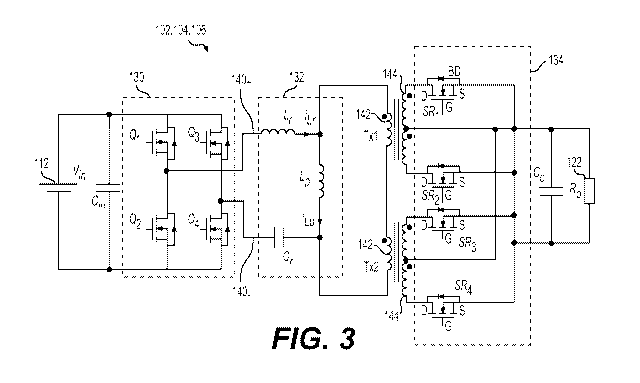
(0027) FIG. 3 is a schematic diagram of an example LLC phase 102, 104, 106
in
accordance with some embodiments of the present disclosure. The example first
LLC phase
102, 104, 106 shown in FIG. 3 may have a construction similar or identical to
any one of the
LLC phases 102, 104, 106 of the multi-phase LLC power converter 100, which may
be
identical to one another, with the exception of differences resulting from
manufacturing
tolerances.
10028] The example LLC phase 102, 104, 106 shown in FIG. 3 includes a
switching
stage 130, a resonant tank 132, a set of transformers Txl, Tx2, and a
rectification stage 134.
The switching stage 130 includes four high-speed switches Ql, Q2, Q3, Q4, with
each of the
high-speed switches being a Gallium Nitride (GaN) high-electron-mobility
transistor (HEMT)
configured to switch the input power to generate a switched power upon a
switched power bus
140+, 140-, the switched power having an approximately sinusoidal (i.e. AC)
waveform
defining a switching frequencyfi., which may also be called an AC frequency or
an AC
switching frequency. In some embodiments, the switching frequency exceeds 300
kHz. In some
embodiments, the switching frequencyfs.' may be varied between 260 and 400
kHz. In some
other embodiments, the switching frequency fm may be varied between 260 and
380 kHz. In
CA 03126832 2021-07-14
WO 2020/154572 PCMJS2020/014911
8
some embodiments, the high-speed switches Q1, Q2, Q3, Q4, may be switched at
an operating
frequency range of between 260 and 380 kHz.
[00291 Each of the four high-speed switches Ql, Q2, Q3, Q4 is configured to
switch
current from a corresponding one of a positive conductor 110-or a negative
conductor 110- of
the input bus 110+, 110- to a corresponding one of a positive conductor 140+
or a negative
conductor 140- of the switched power bus 140+, 140- The switching stage 130
may have a
different arrangement which may include fewer than or greater than the four
high-speed
switches Ql, Q2, Q3, Q4, shown in the example LLC phase 102 shown in FIG. 3.
Each of the
LLC phases 102, 104, 106 within the multi-phase LLC power converter 100 may
have an equal
switching frequency, and the AC waveforms of each of the LLC phases 102, 104,
106 may be
in phase with one another. Alternatively, the AC waveforms of each of the LLC
phases 102,
104, 106 may be out of phase from one another for interleaving the phases and
producing a
smoother output power than if the LLC phases 102, 104, 106 had AC waveforms
that were in
phase with one another.
0030] The resonant tank 132 includes a resonant inductor Lr, a resonant
capacitor Cr,
and a parallel inductance Lp all connected in series with one another between
the switched
power bus 140+, 140_. The transformers Txl, Tx2 each include a primary winding
142, with the
primary windings 142of the transformers Tx I, Tx2 connected in series with one-
another, and
with the series combination of the primary windings 142 connected in parallel
with the parallel
inductance Lp. The parallel inductance Lp may include a stand-alone inductor
device.
Alternatively or additionally, the parallel inductance Lp may include
inductance effects, such as
a magnetizing inductance, of the primary windings 142 of the transformers Txl,
Tx2 Each of
the transformers Tx I, Tx2 has a secondary winding 144 with a center tap
connected directly to
CA 03126832 2021-07-14
WO 2020/154572 PCMJS2020/014911
9
the positive terminal 120+ of the output bus 120-, 120-. The ends of the
secondary windings 144
of the transformers Txl, Tx2 are each connected to the negative terminal 120-
of the output bus
120+, 120_ via a rectifier SR1, SR2, SR3, SR4 in the rectification stage 134.
One or more of the
rectifiers SR1, SR2, SR3, SR4 may take the folui of a switch, such as a field
effect transistor
(FET), operated as a synchronous rectifier, as shown in FIG. 3. Alternatively
or additionally,
one or more of the rectifiers may be formed from one or more different types
of switches, such
as junction transistors, SCRs, etc. Each of the LLC phases 102, 104, 106 may
include a
different number of transformers Txl, Tx2, which may be fewer than or greater
than the two
transformers Txl, Tx2 shown in the example design depicted in the FIGs.
Analysis of the Voltage Across SRs
[00311 For high load current applications, the conduction loss of the
rectifiers SRI,
SR2, SR3, SR4 is proportional to the square of load current in synchronous
rectification LLC
dc-dc converter. Therefore, two transformers Txl, Tx2 with series-connected
input (primary)
windings 142 and parallel-connected output (secondary) windings 144 are
adopted to reduce
current stress of the rectifiers SRL SR2, SR3, SR4, which is shown in FIG. 3
Because the
primary windings 142 of the two transformers Txl, Tx2 are in series, the
current flowing
through the primary windings 142 are the same, and the load current is divided
by the two
transformers Txl, Tx2 and synchronous rectifiers SRL SR2, 5R3, SR4.
[00321 FIG. 4 shows a graph 200 with plots 202, 212, 222, and 232 of
voltages and
currents in an LLC power converter over a common time scale in accordance with
some
embodiments of the present disclosure. Specifically, FIG. 4 includes a first
plot 202 with line
204 of current isRi through the first synchronous rectifier SR1 and line 206
of current isR2
through the second synchronous rectifiers SR2. FIG. 4 also includes a second
plot 212 with line
CA 03126832 2021-07-14
WO 2020/154572 PCMJS2020/014911
214 of the series resonant current Lr through the resonant inductor Li and
line 216 of parallel
resonant current iLp through the parallel inductance L. FIG. 4 also includes a
third plot 222
with line 224 of drain-source voltage Vds,SR1 across the first synchronous
rectifier SRI. FIG. 4
also includes a fourth plot 232 showing an enlarged portion of the third plot
222. The fourth
plot 232 includes line 234a showing an enlarged portion of line 224, when the
drain-source
voltage Vds,sRi first reaches on-threshold voltage VTH ON at time ti, and line
234b showing an
enlarged portion of line 224 when the drain-source voltage Vds,SR1 reaches on-
threshold voltage
VTH ON at time t2 after the ringing is over. The fourth plot 232 also includes
line 236 of gate-
source Vgs,SR1. which functions as the control signal to the first synchronous
rectifier SRi,
indicating a premature turn-on of the first synchronous rectifier SRI at time
ti, and the desired
turn-on of the first synchronous rectifier SRI at time t2, as well as the
desired turn-off of the
first synchronous rectifier SRI at time t3.
l00331 As shown in FIG. 4, at high load current, there is severe voltage
ringing across
SRs between times tO and t2, when the series resonant current iLr is
approximately equal to
parallel resonant current iLp. In SR LLC dc-dc converters, the turn-on time is
usually detected
by the drain-source voltage vas of the corresponding one of the SR switches
SRi, SR2, SR3,
SR4, and thus the voltage ringing can cause the SR switches SRi, SR2, SR3, SR4
to turn-on at
time to, which can cause abnormal and/or inefficient operation.
[00341 FIG. 5A shows an equivalent circuit of the LLC power converter of
FIG. 4
during the voltage ringing, when high-speed switches Ql, Q2, Q3, Q4 are
conducting, and the
SR switches SRi, SR2, SR3, SR4 are turned off The parasitic capacitance C. of
the SR
switches SRI, 5R2, 5R3, 5R4 is in series with the load and with the
corresponding transformer
secondary winding. Because Cr >> C., and ILr = ILp, the equivalent circuit in
FIG. 5A can be
CA 03126832 2021-07-14
WO 2020/154572 PCMJS2020/014911
11
simplified to the circuit shown in FIG. 5B, and the impedance is transferred
into the
transformer primary. At an initial condition (IC), SR switches SR' and 5R3 are
OFF, thus, the
voltage across SR1 and SR3 are each 2Vo, and SR switches 5R2 and SR4 are ON,
the voltage
across these two switches are each 0. If the parasitic capacitors of SRs Coss,
SR are each the
same, the resonant frequency of the RLC circuit is:
c _ _____________________
J r ¨ 1
C,SR=
27-1- (Li, + 41+ 4 oss2
2) \I
n (1)
[00351 The equivalent circuit in FIG. 5B can be further simplified to the
circuit shown
in FIG. 5C. As shown in FIG. 5C, the simplified equivalent circuit can be
regarded as a second-
order network. If the voltage across capacitor it, (i.e. Vds) is selected as
state variables, equation
(2) can be written according to Kirchhoff s Voltage Law (KVL). Characteristic
equation is
described in equation (3), which can be obtained as equation (4). Thus, the
voltage across
capacitor it, is described in equation (5).
d2U du
LC c + RC + u =0=
dt2 C
dt (2)
LCp2 + RCp +1=0. (3)
R ,\I R 1
P1,2 = --2L (TL)2 ¨ ¨LC=
(4)
(5)
tic (t) = Kiev't K 2eP2t.
CA 03126832 2021-07-14
WO 2020/154572 PCMJS2020/014911
12
10036] The initial value of the voltage across capacitor it, and the
current flowing
through inductor IL are given in equations (6). Substituting (6) into (5)
gives equation (7). And
thus uc is given by equation (8). Setting parameters in accordance with
equation (9) provides
equations (10).
uc (0+ ) = tic (0_ ) = 2V
(6)
1L(0,) = ii, (0_ ) = O.
JK,+ K2= 21/0 Ki _ 2p2V0 Pi ¨ __ (7)
LKipi + K2p2 =0 ' p2 - A P2 p1
and K2
2V
____________________________________________ (P2ePli ¨ PteP21 ).
P2 ¨ P1 (8)
R 1 1 R ,
a= 2L ' wo = LC' co==\ I LC (2L)z _ Vat2 _a2 .
(9)
V c
P1,2 = -a .1.0=-0)0/ V and = arctan¨.a (10)
[00371 Substituting equations (9) and (10) into (8) gives equation (11).
1 R7
u LC __ ( )2
I 1 2L
u,(0= 2Voco, e at sin( cot + co) = _______ 2V I 1 sin
(R ), t+ arctan = (11)
co \I1 ( R )2 \ \ LC LC 2L R
LC 2L i
CA 03126832 2021-07-14
WO 2020/154572
PCMJS2020/014911
13
R C ,
<1
10038] If 2 L , the
circuit operates at underdamped, thus there is voltage
ringing across the SRs. And according to equation (11), when the voltage
across capacitor uc is
lower than zero, the SRs are turned on early. In order to address this issue,
an RC equivalent
150 is connected in parallel with the parasitic capacitance of the SRs
2Coss,sk/n2, as shown in
FIG. 6. The RC equivalent 150 may have a resistance of 5100 and a capacitance
value of
100pF, although different values may be used for either or both of the
resistance and/or the
capacitance. In practice, the RC equivalent 150 takes the form of an RC filter
160, 164
connected in parallel with one or more of the SR switches SRI, 5R2, 5R3, 5R4,
as shown in
FIG. 7.
100391 FIG. 7
shows a schematic diagram of a circuit equivalent to the single-phase
LLC power converter shown in FIG 3, with the addition of an RC filter 160,
164, and a
rectifier driver 162, 166 coupled to each of SR1 and SR2. Each of the RC
filters 160, 164
includes a filter resistor Rfl, Rf2 in series with a filter capacitor Cfl, Cu,
with each of the RC
filters 160, 164 connected in parallel across a corresponding one of the SR
switches SR1, SR2.
The filter resistors Rfl, Rf2 each have a resistance of 5100 and the filter
capacitors Cu, Cu each
have a capacitance of 100pF, although different values may be used for either
or both of the
resistance and/or the capacitance. Each of the filter capacitors Cu, Cu
defines a corresponding
filter capacitor voltage Vcfl, Vcf2, which is monitored by a corresponding
rectifier driver 162,
166 and which is compared against a threshold value to control the
corresponding SR switch
SRI_ and SR2. In other words, each of the rectifier drivers 162, 166 are
configured to to drive the
corresponding SR switch SR1, SR2 to a conductive state in response to the
filter capacitor
voltage Vcfl, Vcf2, being less than a threshold voltage VTH ON. The threshold
voltage Vrx ON
CA 03126832 2021-07-14
WO 2020/154572 PCMJS2020/014911
14
may be 0.0V, although other higher or lower voltages may be used as the
threshold voltage
VTH ON.
[00401 To avoid bias current from the SR driver circuit 162, 166 offsetting
the filter
capacitor voltage Val, Vcf2, the value of filter resistors Rfl , Rf2 should be
less than 1ki2.
Besides, the RC time constant should be around 100ns. Each of the SR switches
SRi, SR2, SR3,
SR4 may an RC filter 160, 164 connected thereacross, but FIG. 7 shows RC
filters 160, 164
only on SR switches SRI, SRI to simplify the disclosure. Each of the RC
filters 160, 164
includes a filter capacitor Cfl in series with a filter resistor Rfi. The
filter capacitor Cfl defines a
voltage Val thereacross. The voltage Val across the filter capacitor Cfl may
also be denoted uc,
or Uc,fzltcr and is described in equation (12), below.
1
1
COCfilter (12)
uc,fitter (t) and
(t) Zfi COCfilter
1 fl = ¨ arctan
__________________________ + Rfilter filter
WCfilter
[00411 It can be seen from equation (12), the amplitude of voltage across
filter capacitor
Uc,fiiter is divided by filter capacitor Cfilter and filter resistor Rfilter.
If the voltage across the filter
capacitor ue,fifter is detected to create turn-on signal for SRs, the minimum
of detected voltage
less than zero problem can be solved
100421 Specifications of a single-phase converter in accordance with the
present
disclosure are shown in Table. I.
CA 03126832 2021-07-14
WO 2020/154572 PCMJS2020/014911
TABLE I. SPECIFICATIONS OF ONE PHASE LLC CONVERTER
Via 250 ¨ 430 Lr 25 [tH
VDC
Trout 14 VDC Lp 125 H
Pout/hut 1300 W/90 A Cs 3.4 nF
44: 1 : 1 fsw 260 ¨ 380 KHz
[00431 Table II presents a summary comparison of a proposed LDC in
accordance with
the present disclosure compared with eight different other reference DC-DC
converter designs.
As shown in Table. I, the proposed LDC achieves high efficiency and high power-
density
compared with other LDCs.
TABLE II. COMPARISON BETWEEN THE PROPOSED LDC AND OTHER
REFERENCE DC-DC CONVERTERS
Specification of the Converter
Reference Input Output Peak Full-load Power Switching
Power
voltage voltage efficiency efficiency density frequency
200V-400 0.5kW/
[1] 12V 1.2kW 95.5% 90% 100kHz
V
227kHz-297
[2] 300V 12V 2kW 94% 93.2%
kHz
235V-431 0.94kW
11.5V-15V 2kW 93.5% 93% 200kHz
V /L
300V-400 0.72k
[4] 12V-16V 93.5% 90% 100kHz
V
CA 03126832 2021-07-14
WO 2020/154572
PCMJS2020/014911
16
Specification of the Converter
Reference Input Output Peak Full-load Power Switching
Power
voltage voltage efficiency efficiency density frequency
250V-400
[5] 13V-15V lkW 93% 92% 100kHz
V
220V-450 1.17kW
90kHz-200k
[6] 6.5V-16V 2.5kW 93.2% 92%
/ /L Hz
260V-430 12.5V-14.5 1.02kW
65kHz-150k
171 1.9kW 93% 91%
/ V /L Hz
200V-400 100kHz-
133
[8] 12V 2kW 95.9% 94.2%
/ kHz
The
250V-430 260kHz-
400
proposed 9V-16V 3kW 96.7% 96.2% 3kW/L
/ kHz
LDC
Experimental Results
(0044) To verify the analysis, a 1.26kW prototype is designed. The series
resonant
inductor is 25 H, the parallel inductor is 12501, the resonant capacitor is
3.3nF and
transformer ratio is np:nsl:ns2=22:1:1. Input voltage range is 250V-430V and
output voltage
range is 9V-16V. 90A load current at 14V output voltage is achieved, and SRs
are turned on
properly.
100451 FIG. 8A is a graph 300 showing lines 302, 304, 306 of various
parameters of a
single-phase LLC power converter 102, 104, 106 over a common time scale with
input voltage
Vitt = 250V, output voltage Vout= 14V, and output current Io = 60A.
Specifically, line 302
shows the drain-source voltage Vas across the first SR switch SRI., and line
304 shows the filter
CA 03126832 2021-07-14
WO 2020/154572 PCMJS2020/014911
17
capacitor voltage Vcri of the filter capacitor Cu of RC filter 160. FIG. 8B is
a graph 320
showing lines 322, 324, 326 of various parameters of a single-phase LLC power
converter 102,
104, 106 over a common time scale with input voltage Viii = 380V, output
voltage Vont= 14V,
and output current 10 = 70A. Specifically, line 322 shows the drain-source
voltage Vds across
the first SR switch SRI, and line 324 shows the filter capacitor voltage Val
of the filter
capacitor Cfl of RC filter 160.
10046j As shown in FIGS. 8A-8B, the SRs would be turned on early if the
voltage
across the SR switches SRI, 5R2, 5R3, 5R4 is selected as detected voltage. The
filter capacitor
voltage Val across the filter capacitor Cfl is selected instead and this
problem is solved in the
proposed circuit.
[0047] FIG. 9 is a graph 340 showing lines 342, 344, 346, 346 of measured
efficiency
of a single-phase LLC dc-dc converter with output voltage Vo = 14V and with
SRs operated in
accordance with the present disclosure, using the voltage across the filter
capacitor, /touter.
Specifically line 342 shows the converter operated with input voltage yin =
430V, line 344
shows the converter operated with input voltage Vin = 380V; line 346 shows the
converter
operated with input voltage Vin = 320V; and line 348 shows the converter
operated with input
voltage Vin = 250V. Peak efficiency of 96.99% is realized at 55A load current
when the input
voltage Vin is 380V and the output voltage is 14V.
[0048] FIG. 10 is a graph 360 showing lines 362, 364, 366 of efficiency vs.
output
current of a multi-phase LLC power converter 100 in accordance with some
embodiments of
the present disclosure. Specifically, line 362 shows the multi-phase LLC power
converter 100
operating in a single-phase mode, with only one of the LLC phases 102, 104,
106 operational
Line 364 shows the multi-phase LLC power converter 100 operating in a two-
phase mode, with
CA 03126832 2021-07-14
WO 2020/154572 PCMJS2020/014911
18
two of the LLC phases 102, 104, 106 operational. Line 366 shows the multi-
phase LLC power
converter 100 operating in a three-phase mode, with all three of the LLC
phases 102, 104, 106
operational. FIG. 10 shows the efficiency of the proposed LDC. When the input
voltage yin is
380V and output voltage is 14V, 96.2% efficiency is achieved at 210A load
current. Peak
efficiency is 96.7%. When load current is light, the proposed LDC can run only
one phase LLC
dc-dc converter to reduce switching loss; when load current is medium, the
proposed LDC can
run two phase LLC dc-dc converters; when load current is high, the proposed
LDC can run
three phase LLC dc-dc converters to reduce conduction loss. As shown in FIG.
10, from 10A to
80A, 80A to 150A and 150A to 210A, one phase circuit, two phase circuit and
three phase
circuit are adopted. Thus, high efficiency can be achieved in all load ranges.
[00491 A method 400 of operating an LLC power converter 100 is shown in
the flow
chart of FIG. 11. Actual operation may include additional steps beyond those
listed here. The
method 400 includes sensing a filter capacitor voltage Vcf across a filter
capacitor Cf of a
resistor-capacitor (RC) filter 160 connected across a synchronous rectifier
(SR) switch SR1,
SR2, SR3, SR4 of the LLC power converter 100 at step 402.
(0050) The method 400 also includes comparing the filter capacitor voltage
Vcf with a
threshold voltage VTH ON at step 404. Step 404 may be performed by a
comparator, which may
include hardware, software, or a combination of hardware and software. The
threshold voltage
threshold voltage VTH ON may be 0.0 V, although the threshold voltage VTH ON
may be higher
or lower than 0.0 V. The threshold voltage VTH oN may be fixed or variable.
(0051) The method 400 also includes driving the SR switch SR1, SR2, 5R3,
SR4 to a
conductive state in response to the filter capacitor voltage Vcfbeing less
than the threshold
voltage threshold voltage VTH oN at step 406. Driving the SR switch to the
conductive state
CA 03126832 2021-07-14
WO 2020/154572 PCMJS2020/014911
19
may include asserting or de-asserting a control signal coupled to a gate of
the SR switch SRI,
SR2, SR3, SR4.
[00521 Steps 402-406 may each be performed for each of two SR switches
SRI, SR2,
SR3, SR4 connected to a single secondary winding 144 of a transformer Txl,
Tx2. For
example, as shown in FIG. 7, SR switches SRI, SR2 may each be connected to
opposite ends
of a center-tapped secondary winding 144. Furthermore, Steps 402-404 may each
be performed
for each of four or more different SR switches SRI, SR2, SR3, SR4 within the
LLC power
converter 100. For example, two SR switches SR1, SR2, SR3, SR4 may be
connected to
secondary windings 144 of each of two or more different transformers Txl, Tx2.
10053] The method 400 may also include enabling a number of LLC phases
102, 104,
106 of the LLC power converter 100 less than all of the LLC phases 102, 104,
106 at step 408.
This may be called phase shedding. A controller may enable only as many of the
LLC phases
enabled 102, 104, 106 as are needed to satisfy an output current requirement
of the multi-phase
LLC power converter 100. Satisfying the output current requirement may include
generating an
output current that meets the demand of a load 122. Alternatively or
additionally, satisfying the
output current requirement may include operating the LLC power converter 100
with number
of LLC phases 102, 104, 106 causing the LLC power converter 100 to operate
with a highest
efficiency. For example, and with reference to FIG. 10, the LLC power
converter 100 can be
operated with either of one or two LLC phases to produce an output current of
60A, but one
phase operation is more efficient for the output current of 60A.
(0054) The method 400 may also include switching one or more high-speed
switches
Ql, Q2, Q3, Q4 of a switching stage 130 at a switching frequency1,14.
exceeding 300 kHz at
step 410 to apply a switched power to a resonant tank 132 of the LLC power
converter 100.
CA 03126832 2021-07-14
WO 2020/154572 PCMJS2020/014911
The high-speed switches Q I, Q2, Q3, Q4 may be Gallium Nitride (GaN) high-
electron-
mobility transistors (HEMTs). In some embodiments, the switching frequency fsw
may be
varied between 260 and 400 kHz. In some other embodiments, the switching
frequencyfsw may
be varied between 260 and 380 kHz. In some embodiments, the high-speed
switches Ql, Q2,
Q3, Q4, may be switched at an operating frequency range of between 260 and 380
kHz.
10055] The method 400 may also include supplying an output voltage Vo of
9.0 to 16.0
VDC from an input power having an input voltage Vin of 250 to 430 VDC at step
412.
Conclusions
100561 This disclosure presents a zero-crossing filter for driving
synchronous rectifiers
of LLC DC-DC converters to reduce or eliminate the effect of voltage ringing
across SRs in
high load current applications. In the proposed LLC DC-DC converter, GaN HEMTs
are used
in the switching stage 130, thus switching frequency is greater than in
conventional DC-DC
converters, and the volume of the circuit is reduced. Zero voltage switching
(ZVS) turn-on of
the high-speed switches Ql, Q2, Q3, Q4 and secondary SRs is achieved, zero
current switching
(ZCS) turn-off of secondary SRs is also realized. By detecting the voltage
across the filter
capacitor to create the turn-on signal for SRs, the problem of early SR turn-
on is reduced or
eliminated. In the proposed LLC DC-DC converter, wide input and output voltage
ranges are
realized. Peak efficiency of 96.99% at 55A load current is achieved.
[00571 The system, methods and/or processes described above, and steps
thereof, may
be realized in hardware, software or any combination of hardware and software
suitable for a
particular application. The hardware may include a general purpose computer
and/or dedicated
computing device or specific computing device or particular aspect or
component of a specific
computing device. The processes may be realized in one or more
microprocessors,
CA 03126832 2021-07-14
WO 2020/154572 PCMJS2020/014911
21
microcontrollers, embedded microcontrollers, programmable digital signal
processors or other
programmable device, along with internal and/or external memory. The processes
may also, or
alternatively, be embodied in an application specific integrated circuit, a
programmable gate
array, programmable array logic, or any other device or combination of devices
that may be
configured to process electronic signals. It will further be appreciated that
one or more of the
processes may be realized as a computer executable code capable of being
executed on a
machine readable medium.
(0058) The computer executable code may be created using a structured
programming
language such as C, an object oriented programming language such as C++, or
any other high-
level or low-level programming language (including assembly languages,
hardware description
languages, and database programming languages and technologies) that may be
stored,
compiled or interpreted to run on one of the above devices as well as
heterogeneous
combinations of processors processor architectures, or combinations of
different hardware and
software, or any other machine capable of executing program instructions.
10059.1 Thus, in one aspect, each method described above and combinations
thereof
may be embodied in computer executable code that, when executing on one or
more computing
devices performs the steps thereof In another aspect, the methods may be
embodied in systems
that perform the steps thereof, and may be distributed across devices in a
number of ways, or
all of the functionality may be integrated into a dedicated, standalone device
or other hardware.
In another aspect, the means for performing the steps associated with the
processes described
above may include any of the hardware and/or software described above. All
such permutations
and combinations are intended to fall within the scope of the present
disclosure.
CA 03126832 2021-07-14
WO 2020/154572 PCMJS2020/014911
22
100601 The foregoing description is not intended to be exhaustive or to
limit the
disclosure. Individual elements or features of a particular embodiment are
generally not limited
to that particular embodiment, but, where applicable, are interchangeable and
can be used in a
selected embodiment, even if not specifically shown or described. The same may
also be varied
in many ways. Such variations are not to be regarded as a departure from the
disclosure, and all
such modifications are intended to be included within the scope of the
disclosure.