Note: Descriptions are shown in the official language in which they were submitted.
208273-9011-CA01 (HI 911-0710A CAN)
ENHANCED AUTO-MONITORING CIRCUIT
AND METHOD FOR AN ELECTRICAL DEVICE
This application is a division of application no. 2,809,053 that was filed in
Canada on March 11, 2013.
CROSS-REFERENCE TO RELATED APPLICATIONS
[0001] This application contains subject matter related to subject
matter contained in
copending U.S. Patent Applications filed on even date herewith, application
numbers not
assigned yet, entitled, "SOLENOID COIL HAVING AN ENHANCED MAGNETIC
FIELD," by Stephen P. Simonin, "COMPACT LATCHING MECHANISM FOR
SWITCHED ELECTRICAL DEVICE," by Gaetano Bonasia and Kenny Padro and
"REINSTALLABLE CIRCUIT INTERRUPTING DEVICE WITH VIBRATION
RESISTANT MIS WIRE PROTECTION," by Gaetano Bonasia et al., which applications
are assigned to the assignee hereof.
- 1 -
Date Recue/Date Received 2021-08-13
208273-9011-CA01 (HI 911-0710A CAN)
BACKGROUND OF THE INVENTION
Field of the Invention
[0002] The present application relates generally to switched electrical
devices. More
particularly, the present application is directed to circuit interrupting
devices, such as
ground fault circuit interrupter (GFCI) devices, that switch to a "tripped" or
unlatched
state from a "reset" or latched state when one or more conditions is detected.
Such
devices consistent with the invention disclosed have a more compact latching
mechanism
than conventional devices and provide a reusable feature that electronically
prevents a
miswire condition.
Description of Related Art
[0003] Switched electrical devices having contacts that are biased
toward the open
position require a latching mechanism for setting and holding the contacts in
a closed
position. Likewise, switched electrical devices having contacts that are
biased toward the
closed position require a latching mechanism for setting and holding the
contacts in an
open position. Examples of conventional types of devices include devices of
the circuit
interrupting type, such as circuit breakers, arc fault interrupters and ground
fault circuit
interrupters (GFCI), to name a few. Electrical receptacles having built-in
ground fault
protection circuitry, i.e., GFCI receptacles, are ubiquitous. Such protection
circuitry and
the associated mechanisms normally take up a substantial amount of the
physical space
within a receptacle housing, the size of which is limited by the standard
junction boxes in
which they must fit. The trend toward including additional safety and other
features,
many required by evolving industry standards, has made it necessary to
economize on
interior receptacle space wherever possible.
[0004] GFCI receptacles typically use a mechanical latch for holding
the contacts
closed, and a solenoid, a relay, or some other such actuating device, for
tripping the latch
to open the contacts when an actual fault is detected or when the mechanism of
the device
for detecting such faults is tested. Typical mechanisms for tripping and
resetting the
contacts employ an arrangement in which the axis of the trip solenoid and the
motion of a
- 2 -
Date Recue/Date Received 2021-08-13
208273-9011-CA01 (HI 911-0710A CAN)
linked latch plate are perpendicular to the axis of a reset button and/or
plunger. Despite
the trend toward miniaturization, such arrangements tend to be wasteful of
available
space.
[0005] Additional industry standards for such circuit interrupting
devices, either
presently accepted or contemplated for the future, include: denying power to
the user
accessible and/or downstream load terminals of the device when AC power is
improperly
applied to the load side terminals of the device, known as a miswire
condition; testing for
proper operation of the device after subjecting the device to a sudden force,
known as the
shock, or drop, test; and providing a mechanism by which proper operation of
the device
is periodically confirmed without the need for human intervention, known as
self-test.
Conventional devices that may or may not address one or more of these
additional
industry requirements tend to be too large, ineffective, and/or do not provide
a robust
method for confirming proper functioning of the device.
SUMMARY OF THE INVENTION
[0006] The invention described herein addresses the issues mentioned
above
regarding conventional circuit interrupting devices. Specifically, the
invention described
employs a space-efficient configuration in which the mechanical latching
arrangement for
resetting (closing) the contacts is disposed inside the trip solenoid, and the
reset plunger
and the solenoid are coaxial. A device according to other aspects of the
invention further
includes industry compliant means for preventing the miswire condition and
automatically testing, among other things, its own ability to detect faults.
[0007] A circuit interrupting device according to one aspect of the
invention includes
a pair of conductive line terminals for connecting to an AC power source, a
pair of line
conductors each being electrically coupled to a respective one of the
conductive line
terminals, a test conductor electrically isolated from the pair of line
conductors and a
pair of conductive face terminals configured to receive mating conductors of
an electrical
load. A fault detection circuit is further included that has at least one
transformer coil
through which each of the pair of line conductors and the test conductor
traverse, the fault
- 3 -
Date Recue/Date Received 2021-08-13
208273-9011-CA01 (HI 911-0710A CAN)
detection circuit being configured to detect a net current passing through the
at least one
transformer and generate a fault detection signal. The circuit interrupting
device also has
an interrupting device operable to electrically couple the pair of line
conductors and the
pair of face terminals, an actuator operable to engage the interrupting device
to
electrically decouple the pair of line conductors and the pair of face
terminals and an
auto-monitoring circuit electrically coupled to the fault detection circuit
and the actuator,
wherein the auto-monitoring circuit generates a test net current on the test
conductor and
determines whether the fault detection circuit successfully detects the test
net current
passing through the at least one transformer coil.
[0008] A circuit interrupting device according to a further aspect of
the invention
includes two sets of electrical contacts, each set of electrical contacts
having a fixed
contact and at least one movable contact biased away from the fixed contact, a
latch
assembly including a carriage operable to hold one of the movable contacts
from each of
the sets of electrical contacts, and first and second sets of rigid beams, a
reset assembly
including a user accessible reset button and a plunger having a reset flange
with an upper
surface and a lower surface, the upper surface engaging the first set of rigid
beams when
the reset button is pressed and the lower surface engaging the second set of
rigid beams
when the reset button is released and an auto-monitoring circuit electrically
coupled to
the latch and reset assemblies, wherein the auto-monitoring circuit is
configured to
automatically determine whether the circuit interrupting device is operating
properly.
[0009] According to another aspect of the invention an auto-monitoring
circuit for
automatically monitoring the performance of a ground fault circuit
interrupting (GFCI)
device is provided that includes a microprocessor configured to periodically
run an auto-
monitoring routine based on a stored program with a driver coupled to the
microprocessor and being operable to initiate a test signal representative of
a ground fault
each time the auto-monitoring routine is performed, or run. An end-of-life
indicator is
coupled to the microprocessor which is operable to indicate that the GFCI
device has
failed to detect the test signal in a predetermined number of consecutive runs
of the auto-
monitoring routine. The microprocessor directly drives the end-of-life
indicator.
- 4 -
Date Recue/Date Received 2021-08-13
208273-9011-CA01 (HI 911-0710A CAN)
[0010] According to yet a further aspect of the invention a method is
provided for
operating and testing a ground fault circuit interrupter. The method includes
periodically
running an auto-monitoring routine during which a test current is passed
through a sense
transformer. The method also includes generating a secondary current at the
sense
transformer when the test current passes through the sense transformer,
detecting the
secondary current, generating first and second detection signals when the
secondary
current is detected and measuring the second detection signal. To carry out
the method
according to this aspect additional steps of determining if the test current
was
successfully detected based on a result of the measuring the second detection
signal,
generating a fail count based on the result of the determining step, the fail
count
representing a number of times the periodic test current was not detected,
tripping the
circuit interrupting device if the fail count reaches a predetermined
threshold within a
predetermined amount of time, and preventing the circuit interrupting device
from being
tripped by the first detection signal if the fail count reaches a
predetermined threshold
within a predetermined amount of time, are conducted.
[0011] According to yet a further aspect of the invention a circuit
interrupting device
is provided that includes a hot conductive line terminal for connecting to the
hot
conductor of an AC power source and a neutral conductive line terminal for
connecting to
the neutral conductor of an AC power source. A line conducting means is
included for
carrying current either from or to each of the hot conductive line terminal
and the neutral
conductive line terminal. A detection means is also included for detecting a
net current
passing through a transformer and generating a detection signal when such a
detection
occurs. Also, a test conductor means that is electrically isolated from the
line conducting
means is included for carrying a test net current through the transformer, and
an auto-
monitoring means is included for generating the test net current and
determining if the
detection means is successfully detecting the test net current.
- 5 -
Date Recue/Date Received 2021-08-13
208273-9011-CA01 (HI 911-0710A CAN)
BRIEF DESCRIPTION OF THE DRAWINGS
[0012] Exemplary embodiments of the disclosed invention are described
in detail
below by way of example, with reference to the accompanying drawings, in
which:
[0013] FIG. 1 is a front perspective view of a GFCI receptacle
incorporating the
resettable switching apparatus of the invention;
[0014] FIG. 2 is a rear perspective view of the GFCI receptacle shown
in FIG. 1;
[0015] FIG. 3 is an exploded front perspective view of the receptacle
of FIG. 1;
[0016] FIG. 4 is a front perspective view of the receptacle of FIG. 1,
with the front
and rear covers and tamper-resistant mechanisms removed;
[0017] FIG. 5 is a rear perspective view of the receptacle depicted in
FIG. 4;
[0018] FIG. 6 is a rear perspective view of the ground yoke/bridge
assembly of the
receptacle of FIG. 1;
[0019] FIG. 7 is a front perspective view of the core assembly of the
receptacle of
FIG. 1;
[0020] FIG. 8 is a front perspective view similar to FIG. 7 from a
different angle,
with bus bars and other components added;
[0021] FIG. 9 is a front perspective view similar to FIG. 7 with test
and reset buttons
and other components added;
[0022] FIG. 10 is a front perspective view similar to FIG. 8 from a
different angle,
with some parts removed and others added;
[0023] FIG. 11 is a front perspective view in transverse cross-section
of the
receptacle in the tripped or unlatched state taken along line 11-11 in FIG. 1;
[0024] FIG. 12 is a bottom perspective view of the solenoid used in the
receptacle of
FIG. 1;
[0025] FIG. 13 is a top perspective view of a contact carriage used in
the receptacle
of FIG. 1;
[0026] FIG. 14 is a bottom perspective view of the contact carriage of
FIG. 13;
- 6 -
Date Recue/Date Received 2021-08-13
208273-9011-CA01 (HI 911-0710A CAN)
[0027] FIG. 15 is a side elevational view in transverse cross-section
view of the
contact carriage of FIG. 13 taken along line 15-15;
[0028] FIG. 16 is an end elevational view in transverse cross-section
of the contact
carriage of FIG. 13 taken along line 16-16;
[0029] FIG. 17 is an exploded rear perspective view of the contact
carriage of FIG.
13;
[0030] FIG. 18 is a rear perspective view of the reset button assembly
used in the
receptacle of FIG. 1;
[0031] FIG. 19 is a side elevational view in transverse cross-section
of the reset
button assembly of FIG. 18 taken along line 19-19;
[0032] FIGS. 20, 22, 23, 25 and 26 are front elevational views in
transverse cross-
section similar to FIG. 11 showing an alternate version of the latching
components of the
receptacle in progressive states during the resetting process;
[0033] FIG. 21 is a front elevational view in cross-section of the
state of the latching
components shown in FIG. 20 taken along line 21-21;
[0034] FIG. 24 is a front elevational view in cross-section of the
state of the latching
components shown in FIG. 23 taken along line 23-23; and
[0035] FIG. 27 is a schematic diagram of an exemplary circuit that may
be employed
in the receptacle of FIG. 1.
DETAILED DESCRIPTION OF EXEMPLARY EMBODIMENTS
[0036] As described herein, terms such as "front," "rear," "side,"
"top," "bottom,"
"above," "below," "upwardly" and "downwardly" are intended to facilitate the
description of the electrical receptacle of the invention, and are not
intended to limit the
structure of the invention to any particular position or orientation.
[0037] Exemplary embodiments of devices consistent with the present
invention
include one or more of the novel mechanical and/or electrical features
described in detail
below. Such features include a compact latching mechanism that efficiently
utilizes the
space within the device housing to provide additional area for additional
features and/or
- 7 -
Date Recue/Date Received 2021-08-13
208273-9011-CA01 (HI 911-0710A CAN)
components. For example, certain types of GFCI devices accommodate a separate
plug
on the back side of the device for connecting AC power to the device (e.g.,
SNAPConnectO devices by Hubbell Incorporated). To accommodate the additional
plug
it is beneficial to reconfigure certain components within the device housing,
such as the
latching mechanism, and make more efficient use of the given space in the
housing. One
feature consistent with this objective is to provide a solenoid for actuating
the latching
mechanism that is coaxial with the reset pin.
[0038] In addition to providing a space-saving mechanical configuration
for the
devices, the present invention further includes novel electrical features as
well. For
example, one or more of the exemplary embodiments of the invention include an
electrical miswire feature that prevents the device from being reset, or
latached, until the
AC power is properly connected to the device, i.e., on the line side of the
device as
opposed to the face, or load, side. In comparison to mechanical type miswire
prevention
mechanisms, an electrical solution such as provided with the present invention
avoids
inadvertent failure of the mechanical miswire mechanism due to, for example,
dropping
the device prior to installation. Additional electrical features are also
provided in
accordance with exemplary embodiments of the invention, such as, enhanced self-
test, or
auto-monitoring, features.
[0039] Some self-test features and capabilities with respect to GFCI
devices have
been disclosed previously, for example, in U.S. patent nos. 6,807,035,
6,807,036,
7,315,437, 7,443,309 and 7,791,848, of which U.S. patents may be referred to
for further
details. An auto-monitoring feature consistent with the present invention is
more robust
than that which has been previously disclosed. For example, additional
features are
provided related to the determination of an end-of-life (EOL) condition and
actions taken
subsequent to such determination. Further exemplary novel electrical and
mechanical
features consistent with the invention are described herein below with
reference to the
figures.
[0040] Referring to FIGS. 1 and 2, a GFCI receptacle 10 according to
the invention
comprises a front cover 12 having a duplex outlet face 14 with phase 16,
neutral 18 and
ground 20 openings. The NEMA-standard T-shaped phase openings 16 indicate that
this
- 8 -
Date Recue/Date Received 2021-08-13
208273-9011-CA01 (HI 911-0710A CAN)
particular exemplary embodiment is rated for 20 ampere operation. Face 14 also
has a
central opening 22 for a reset button 24 flanked by an opening 26 for a test
button 28 and
an opening 30 for concentric status indicators 32, 34. Rear cover 36 is
secured to front
cover 12 by four screws 38. Ground yoke/bridge assembly 40 having standard
mounting
ears 42 protrudes from the ends of the receptacle.
[0041] Referring to FIG. 3, the exemplary embodiment shown incorporates
two
tamper-resistant mechanisms 44 disposed behind face 14, one for each outlet of
the
duplex receptacle. The structure and operation of these tamper-resistant
mechanisms are
disclosed in U.S. Patent No. 7,510,412 to Valentin, which issued on March 31,
2009,
the contents of which may be referred to for further details.
[0042] Referring to FIGS. 2 and 5, the exemplary GFCI receptacle 10
shown includes
plug-in arrangement 50 for connection to a source of electricity. This
arrangement
comprises line terminals in the form of a phase blade 52, a neutral blade 54
and a ground
blade 56 located in a contoured recess 58 in the back of rear cover 36. The
source
connection is made when a mating plug (not shown) wired to an AC power source
is
plugged into mating recess 58. According to an alternative embodiment,
standard wire-
insertion and/or screw line terminals may be used instead of plug-in
arrangement 50.
Such an alternative embodiment requires additional push-in contact holes
and/or terminal
screws not shown.
[0043] Referring to FIG. 6, ground yoke/bridge assembly 40 comprises a
main full-
length member 60 having two rectangular apertures 62 and a round central
aperture 64.
A ground plate 66 carrying two face ground terminals 68 is riveted, or
otherwise securely
fixed, to main section 60. Ground plate 66 also has a substantially round hole
70 in
registry with aperture 64 of main full-length member 60, through which part of
a solenoid
coil bobbin and part of a reset button assembly extends when the device is
fully
assembled, as noted in more detail below. Ground blade 56 is riveted or
otherwise
securely fixed to a bent tab 72 on main member 60. An auxiliary grounding
plate 74 is
also provided.
[0044] Referring to FIG. 7, core assembly 80 includes circuit board 82
that supports
most of the working components of the receptacle, including the GFCI circuit
(see FIG.
- 9 -
Date Recue/Date Received 2021-08-13
208273-9011-CA01 (HI 911-0710A CAN)
27), sense transformer 84 and grounded neutral transformer 85. AC line power
is
delivered via phase conductor bar 86 and neutral conductor bar 88, which
respectively
carry at their ends phase blade 52 and neutral blade 54. Conductors 86 and 88
are
received in holes in circuit board 82 and are connected on the underside of
board 82 (see
FIG. 5) to oblique linking conductors 90, 92, respectively. Line contact arms
94, 96
connect to oblique linking conductors 90, 92, respectively, and pass through
transformers
84, 85 with an insulating separator 98 therebetween. Line contact arms 94, 96
are
cantilevered, their respective distal ends carrying phase and neutral line
contacts 102,
104, adjacent solenoid 108. The resiliency of the cantilevered contact arms
biases the
line contacts 102, 104 toward a lowered (i.e., open) position where they may
rest on a
movable contact carriage 106, made of insulating (preferably thermoplastic)
material, that
surrounds or substantially surrounds solenoid 108.
[0045] Referring to FIGS. 8 and 10, phase and neutral face terminals
110, 112 are
energized through bus bars 114, 116, respectively. Bus bars 114, 116 have
respective,
relatively short, contact arms 118, 120, which carry at their distal ends
contacts 122, 124
aligned with their respective movable line contacts 102, 104. As seen, for
example, in
FIGS. 3 and 4, core assembly 80 is substantially surrounded by an insulating
separator
manifold 126, which also serves to compaiimentalize i.e., separate, face
terminals 110,
112 and bus bars 114, 116.
THE TRIP AND RESET MECHANISM
[0046] The components of the trip and reset mechanism will now be
described.
Referring to FIGS. 11 and 12, solenoid 108 includes a coil bobbin 130 having
four
standoffs 132, which space the solenoid from circuit board 82. Conductive pins
134, 136,
138 extend through three of the standoffs and penetrate circuit board 82 where
they are
soldered to separate circuit leads (not shown), anchoring the solenoid to the
circuit board.
Two concentric coils, preferably of the same wire gauge, are wound in series
in the same
direction, "W" (see FIG. 12), around bobbin 130 comprising an inner coil 140
preferably
having about 600 turns, and an outer coil 142 preferably having about 320
turns.
Winding of the two concentric coils begins at pin 134, to which the inner end
of inner
- 10 -
Date Recue/Date Received 2021-08-13
208273-9011-CA01 (HI 911-0710A CAN)
coil 140 is connected, and proceeds to pin 136, to which the outer end of
inner coil 140 is
connected. Winding continues in the same direction with the inner end of outer
coil 142,
which is also connected to pin 136, and proceeds to pin 138, to which the
outer end of
outer coil 142 is connected. A layer of tape covers outer coil 142.
[0047] As explained more fully below, tripping of the GFCI device in
the event of a
fault employs an enhanced electromagnetic force combining the force from both
coils
140, 142 in series by causing a voltage to be applied across pins 134 and 138.
Both coils
are also energized during reset, when reset switch contact pads 144 on circuit
board 82
are electrically connected together as described below. Fail-safe tripping of
the GFCI
device in the event of a malfunction, however, involves only inner coil 140 by
causing a
voltage to be applied across pins 134 and 136, creating a power-denial, end-of-
life
condition, described further below.
[0048] Referring to FIGS. 13-17, contact carriage 106 includes a
substantially tube-
like, or cup-like, body 150 having a central recess 152 dimensioned to
slidably surround
solenoid 108. An end or bottom wall 154 of body 150 has four holes 156
positioned and
sized to slidably accommodate standoffs 132 of solenoid 108. External wings
158, 160
of body 150 have respective recesses 162, 164, which are configured to cradle
movable
line contacts 102, 104, respectively, alongside and adjacent to solenoid 108.
[0049] Bottom wall 154 of carriage 106 has on its underside two blind
holes 180 in
which coil springs 182 are seated. Coil springs 182, which abut circuit board
82 (see
FIG. 11), are frictionally retained in holes 180 by virtue of the reduced-
diameter inner
end 181 of each hole (see FIG. 15). Bottom wall 154 also has a central hub 184
that
projects upwardly into recess 152. Central hub 184 has four slots 186 and a
central
locating pin 188 on its underside, as best seen in FIG. 17. The underside of
bottom wall
154 also has a flat channel 179, and two anchoring studs 189 for attaching the
parts
described below. Attachment of these parts involves heating and flattening
anchoring
studs 189 to lock all of the parts together, as seen in FIGS. 14 and 16. In
the exploded
view of FIG. 17, however, which illustrates assembly of the parts, anchoring
studs 189
are depicted in their pre-deformed state.
- 11 -
Date Recue/Date Received 2021-08-13
208273-9011-CA01 (HI 911-0710A CAN)
[0050] Referring to FIG. 17, leaf spring contact assembly 170,
comprising a single
integral member in the embodiment shown, is attached to the underside of
bottom wall
154. Assembly 170 preferably has two pair of conductive leaf spring contacts
172
cantilevered outwardly from a central mounting plate 174, which has two
mounting holes
176 and a central locating hole 178. When assembled, mounting plate 174 is
seated in
channel 179, with locating pin 188 in locating hole 178 and anchoring studs
189 in
mounting holes 176. In their relaxed state, leaf spring contacts 172 depend
from bottom
wall 154 at a shallow angle, with their distal portions directly above reset
contact pads
144 on circuit board 82. Except for instances when reset button 24 is pressed,
the leaf
spring contacts 172 remain above circuit board 82, spaced from reset contact
pads 144
(see FIG. 11).
[0051] A latch beam assembly 190, comprising a single integral member
in the
embodiment shown, is also attached to the underside of bottom wall 154. Latch
beam
assembly 190 includes a pair of opposed latch beams 192 that project upwardly
from a
central mounting plate 194 which abuts mounting plate 174 of leaf spring
contact
assembly 170. Mounting plate 194 has two mounting holes 196 which receive
anchoring
studs 189, a central locating hole 198 which receives locating pin 188, and
two lateral
locating apertures 199. Latch beams 192 extend upwardly through a pair of
opposed
slots 186 in central hub 184. Each latch beam 192 is transversely resilient
and has an
inwardly and downwardly directed latch tab 200 just below a slightly flared
tip 202,
defining a latching shoulder 204 that faces generally downward as seen, for
example, in
FIGS. 15-17.
[0052] A pair of opposed, transversely resilient reset beams 206 extend
upward
through the other pair of opposed slots 186 in central hub 184. Reset beams
206, in this
embodiment, are made of a unitary, one-piece member having a mounting bight
portion
208 with opposed locating tabs 210 and a central locating hole 212. When
assembled,
the upper surface of bight portion 208 abuts the underside 185 of central hub
184, with
locating pin 188 in locating hole 212. The lower surface of bight portion 208
abuts
mounting plate 194 of latch beam assembly 190, with locating tabs 210
resiliently
retained in locating apertures 199. Each reset beam 206 has an inwardly and
upwardly
- 12 -
Date Recue/Date Received 2021-08-13
208273-9011-CA01 (HI 911-0710A CAN)
directed reset tab 214 just below a slightly flared tip 216, defining a reset
shoulder 218
that faces generally upward as seen in FIGS. 15-17.
THE RESET BUTTON ASSEMBLY
[0053] FIGS. 11, 18 and 19 depict details of the reset button assembly
according to
one exemplary embodiment of the invention. Reset button 24 has four depending
side
walls 220 surrounding a round central boss 222, which defines, with the side
walls 220,
an annular seat 224 for a reset spring 226. Each of the two side walls, which
are parallel
to the sides of the receptacle, has an outwardly facing retaining tab 228. A
reset plunger
230 is fixed to reset button 24 in blind hole 229 within central boss 222.
Reset plunger
230 comprises an elongated upper section 232 of substantially uniform and
constant
diameter, a wider relatively short middle section 234 having an upper shoulder
236, and a
narrower lower section 238 having a tapered tip 240. Lower section 238 also
has an
intermediate collar 241 approximately as wide as middle section 234 with an
upper
shoulder 242 and a lower shoulder 244. A hollow ferrous armature 250 surrounds
and is
movable along reset plunger 230. Armature 250 has a frustoconical lower end
252 and
an upper inner shoulder 254. Armature return spring 48, retained between
shoulders 254
and 236, urges armature 250 upwardly to abut central boss 222 when at rest. As
seen in
FIG. 11, retaining tabs 228 of reset button 24 are captured beneath adjacent
portions of
the face 14 of front cover 12 (when in the tripped or unlatched state) while
reset spring
226 rests against ground plate 66 to urge reset button 24 and the attached
reset plunger
230 upwardly.
THE RESET OPERATION
[0054] The reset operation of a device in accordance with the present
exemplary
embodiment will now be described with reference to FIGS. 20-26. Some of the
latching
components depicted in these figures are slightly modified as compared to
those depicted
in the earlier figures. Specifically, the embodiment depicted in FIGS. 20-26
has a larger
armature 250, and a longer collar 241 on plunger 230. Further, one of the
reset beams
206 has a downwardly (instead of upwardly) directed tab 215 (see FIGS. 21 and
24),
- 13 -
Date Recue/Date Received 2021-08-13
208273-9011-CA01 (HI 911-0710A CAN)
which functions similarly aslatch tabs 200 on latch beams 206, thus providing
a greater
bite on upper shoulder 242 of collar 241 during latching.
[0055] FIGS. 20 and 21 illustrate the tripped or unlatched state (open
contacts 102,
122 and 104, 124) just prior to initiating the reset sequence. In this state,
reset button 24
is in its highest position relative to the face 14 of the housing and
protruding with tabs
228 abutting the underside of front cover 12, which is indicative to a user
that the device
is in the tripped state. Collar 241 nests between the upper portions of latch
beams 192
and reset beams 206, with its lower shoulder 244 just above the upper edge 218
of reset
tab 214 (see FIG. 21). Contact cradle 106 is supported solely by springs 182,
which keep
leaf spring contacts 172 spaced from reset contact pads 144 on circuit board
82.
[0056] FIG. 22 illustrates the condition of the latch components of
FIGS. 20 and 21
when reset button is initially being pressed. Specifically, when reset button
24 is pressed,
lower shoulder 244 of collar 241 engages the upper edge 218 of reset tab 214
(see FIG.
21), forcing reset beam 206 and the attached contact carriage 106 downward
until leaf
spring contacts 172 electrically connect reset contact pads 144 on circuit
board 82. This
closes a reset circuit which ultimately activates, or energizes, solenoid 108
to fire on a
positive half-cycle of the AC waveform. Further details of the operation of
the reset
circuit and other electrical operations of exemplary GFCI devices according to
the
invention are provided below in reference to FIGS. 27 and 28.
[0057] Referring again to FIGS. 22-26, as the energized solenoid pulls
armature 250
downward against the bias of spring 256 (see FIGS. 22, 23 and 24), tapered
lower end
252 of the armature spreads apart latch beams 192 and reset beams 206, freeing
reset tab
214 from lower shoulder 244 of collar 241. With pressure still exerted on
reset button 24
by the rear, reset plunger 232, including collar 241, move further downward
(see FIG. 25)
until upper shoulder 242 of collar 241 clears latch tabs 200 on latch beams
192 and tab
215 on reset beam 206. On the negative, non-firing, half-cycle of the AC
waveform,
solenoid 108 is instantly de-energized, allowing the compressed armature
return spring
256 to retract armature 250. It should be noted that although the present
embodiment
contemplates the solenoid to be activated on the positive half-cycle of the AC
waveform
when the reset button is pressed and de-activated on the negative half-cycle,
it is also
- 14 -
Date Recue/Date Received 2021-08-13
208273-9011-CA01 (HI 911-0710A CAN)
within the scope of the invention that solenoid activation occur on the
negative half-cycle
and de-activation on the positive half-cycle. One having skill in the art
would appreciate
how to invert the AC waveform for this purpose, for example, by selectively
placing a
diode in the reset circuit.
[0058] With armature 250 no longer between latch beams 192 and reset
beams 206,
the beams spring back under their natural bias to their original positions,
i.e., they spring
inward toward each other as shown in FIG. 25. Because collar 241 is now below
latch
tabs 200, lower edges 204 of latch tabs 200 (see FIG. 16) and the lower edge
of tab 215
engage the upper shoulder 242 of collar 241. With no downward force now being
applied to the contact carriage 106 via reset beam 206, coil springs 182 raise
the contact
carriage to disengage leaf spring contacts 172 from reset contact pads 144,
thus
preventing further energizing of the solenoid. Also, armature 250 rises under
the return
bias of spring 256. In this "pre-latched" state (see FIG. 25), the movable
contacts 102,
104 have moved closer to their respective fixed contacts 122, 124, but have
not yet closed
with them, i.e., they have not contacted them.
[0059] The impact of the top of retracting armature 250 on the
underside of reset
button 24 provides a tactile indication to the user that reset button 24 can
be released.
When reset button 24 is released, reset return spring 226 pulls the reset
button assembly,
including collar 241, latch tabs 200 and the now latched contact carriage 106,
upward
until contacts 102, 122 and 104, 124, respectively, are closed (see FIG. 26).
In this fully
reset state, latch tabs 200, which abut upper shoulder 242 on reset plunger
232, hold reset
button 24 nearly flush with the face 14 of the receptacle, indicating that the
device is in
the latched, or reset state. This is in comparison to FIG. 20, which shows the
highest
position of reset button 24 when in the unlatched, or tripped, state.
[0060] According to another embodiment, the above-described reset
arrangement can
be incorporated in a GFCI-protected receptacle that also has load terminals
for supplying
power to downstream devices. For example, such an alternative embodiment is
readily
accomplished by providing an additional set of phase and neutral contacts at
the ends of
additional respective cantilevered load-side contact arms, which connect to
load
terminals, such as terminal screws or push-in contact holes, as described
above in regard
- 15 -
Date Recue/Date Received 2021-08-13
208273-9011-CA01 (HI 911-0710A CAN)
to line side terminals. In an exemplary arrangement, one such load contact is
positioned
below movable line contact 102 on the phase side of the device, and the other
load
contact is positioned below movable line contact 104, on the neutral side of
the device.
With the receptacle in the tripped or unlatched state, all contacts on each
side (phase and
neutral) are electrically isolated. During the reset operation the movable
load contacts
rise first, by movable contact carriage 106, and engage their respective line
contacts 102,
104, which then rise to engage their respective fixed (face-connected)
contacts 122, 124.
Alternatively, the positions of the movable load and line contacts could be
reversed.
[0061] A receptacle according to aspects of the invention also includes
components
for testing the GFCI circuitry and permanently denying power to the face
terminals and to
the load terminals, if so equipped, when a malfunction is detected. The
arrangement
according to one embodiment utilizes a two-stage switch, actuated by pressing
the test
button, which is functionally similar to a switch disclosed in U.S. Patent No.
6,697,238 to
Bonilla, et al., which issued on February 24, 2004 and which may be referred
to for
further details. The first stage of the test switch closes primary contacts
that cause the
GFCI supervisory circuit to simulate a ground fault. If the device
malfunctions, for
example, it does not trip/unlatch by energizing the solenoid, continued
pressing of the test
button invokes the second stage, which closes secondary contacts in a simple
circuit that
energizes the solenoid to trip and unlatch the device and blow a fuse to
permanently
disable the device (an end-of-life condition).
[0062] Referring to FIGS. 4, 8 and 9, vertically movable test button 28
is disposed
above L-shaped conductive spring arm 260, the lower (vertical) leg 262 of
which is
anchored in a recess in separator manifold 126. The upper (horizontal) leg 264
of spring
arm 260 is cantilevered with its free, distal, end 266 disposed above the top
268 of a
rocker contact 270. One leg 272 of rocker contact 270 is supported on a lead
274 of a
resistor mounted on circuit board 82. The other leg 276 of rocker contact 270
is disposed
adjacent one end 280 of a test jumper 282, which is supported at its other end
284 on
another resistor lead 286. A test jumper wire 288 electrically connects spring
arm 260 to
neutral bus bar 116.
- 16 -
Date Recue/Date Received 2021-08-13
208273-9011-CA01 (HI 911-0710A CAN)
[0063] When test button 28 is pressed, the distal end 266 of spring arm
260 makes
contact with the top 268 of rocker contact 270, closing the test circuit,
e.g., to simulate a
fault, as described in more detail below. If the device malfunctions, i.e.,
does not
trip/unlatch by energizing the solenoid, continued pressing of the test button
causes leg
276 of rocker contact 270 to swing out and contact the end 280 of test jumper
282. When
this occurs, both inner and outer coils 140, 142 of solenoid 108 are energized
to trip and
unlatch the device. Further, under this condition, an open circuit is
generated, such as by
blowing a fuse, to permanently disable the device. According to one aspect of
this
exemplary embodiment, an end-of-life indicator, such as a red LED on circuit
board 82,
is activated to indicate the end-of-life status. The glow of the red end-of-
life LED is
visible on the face 14 through outer light pipe 34 (see FIGS. 1, 3, 4 and 5).
TRIPPING THE GFCI DEVICE
[0064] Tripping, or unlatching, the device and, thus, opening contacts
102, 122 and
104, 124, will now be described with reference to FIGS. 20, 23 and 26. FIG.
26, for
example, illustrates the major components of a GFCI device in accordance with
embodiments of the invention. More particularly, FIG. 26 illustrates the
latching
components in the fully reset state, i.e., with the line and face contacts
electrically
connected. When solenoid 108 is momentarily energized by one or more of a
detected
fault, a simulated fault or as a result of another test, or by the fail-safe
circuit during
testing as a result of an end-of-life condition, a magnetic field is generated
and solenoid
armature 250 is biased or pulled, e.g., downward in FIG. 23, thus, spreading
apart latch
beams 192 and reset beams 206 (see also FIG. 23). This action frees latch tabs
200 from
upper shoulder 242 of reset plunger 232, thus, unlatching carriage 106 and
allowing reset
spring 226 to raise reset plunger 232 by pushing upward against reset button
24. Carriage
106 is now free to move and drops due to the natural downward bias of contact
arms 94,
96 with movable contacts 102, 104 which rest within recesses 162, 164 (see
FIG. 13).
When movable contacts 102, 104 move downward, they separate from their
respective
fixed (face) contacts 122, 124. FIG. 20 illustrates the mechanism shown in
FIG. 23 in the
final unlatched, tripped, state with carriage 106, including contacts 172,
supported above
- 17 -
Date Recue/Date Received 2021-08-13
208273-9011-CA01 (HI 911-0710A CAN)
the circuit board and contact pads 144 by coil springs 182. In this state,
reset button 24 is
in its highest position relative to the front face of the device housing.
THE POWER-ON STATUS INDICATOR
[0065] A power-on status indicator in the form of a green LED 290 (see
FIG. 8) is
visible on face 14 through inner light pipe 32 (see FIGS. 1, 3, 4 and 5). LED
290 is
mounted on a mini-PCB 292, and is electrically connected to neutral bus bar
116 by its
lead 294 and electrically connected to phase bus bar 114 by a jumper 296.
Further details
of the operation of the power-on status indicator are provided below in
reference to FIG.
27.
[0066] FIG. 27 is a schematic of an electrical circuit consistent with
one or more of
the exemplary embodiments of the present invention described above. More
particularly,
the circuit shown in FIG. 27 can be employed in a GFCI device as described
above with
respect to various embodiments of the invention. The circuit shown in FIG. 27
is
consistent with the mechanical operation of the invention described above;
however, a
GFCI device consistent with the invention need not employ the precise
electrical circuit
depicted in FIG. 27 and those of ordinary skill in the art, after viewing FIG.
27 and/or
reviewing the description set forth below, would be able to modify certain
aspects of the
circuit to achieve the same or similar results. Such modifications are
contemplated and
believed to be within the scope of the invention set forth herein.
[0067] Referring to FIG. 27, an electrical circuit consistent with the
operation of the
present invention includes phase line terminal 326 and neutral line terminal
328 for
electrical connection to an AC power source (not shown). Phase conductor 330
and
neutral conductor 332 are respectively connected to the phase and neutral line
terminals
and each pass through sense transformer 334 and grounded neutral transformer
336,
which are part of a detection circuit described below. By way of example,
phase and
neutral line conductors 330, 332 represent line contact arms 94, 96,
respectively, as
described above with respect to one exemplary embodiment of the invention.
Line
conductors 330, 332 are each cantilevered with respective fixed ends connected
to the
line terminals and each includes a respective movable contact, e.g. contacts
102, 104
- 18 -
Date Recue/Date Received 2021-08-13
208273-9011-CA01 (HI 911-0710A CAN)
from the embodiment described above. Face phase and face neutral conductors
338, 340,
respectively, include electrical contacts, for example contacts 122, 124 in
the
embodiment above, fixed thereto. The face conductors are electrically
connected to and,
in the embodiment shown are integral with, respective face terminals 342, 344,
to which
plug blades would be connected when the electrical receptacle device is in
use.
[0068] The circuit shown in FIG. 27 also includes optional load phase
and load
neutral terminals 346, 348, which electrically connect to a downstream load,
such as one
or more additional receptacle devices. Load terminals 346, 348, when included,
are
respectively connected to cantilevered load conductors 277, 278, each of which
includes
a movable contact (not shown) at its distal end. The load contacts are
disposed between
respective phase and neutral line contacts and phase and neutral face contacts
and are
coaxial with them such that when one of the pairs of conductors, i.e., line or
load, is
moved toward the other, i.e., load or line, and the face conductors, the three
sets of
contacts will mate and be electrically connected together, e.g., in the reset
state described
above.
THE DETECTOR CIRCUIT
[0069] A detector circuit 352 includes transformers 334, 336 as well as
a GFCI
integrated circuit device (GFCI IC), 350. GFCI IC 350 can be one of an RV4141
or
RV4145 device, both made by Fairchild Semiconductor Corporation, a Fudan
FM2141
device, a Crys-Lattice CL4141 device, or it can be a custom device or circuit.
GFCI IC
350 receives electrical signals from transformers 334, 336 and determines if
one or more
faults, either real or simulated, has occurred. For example, when a current
imbalance in
line conductors 330, 332 occurs, a net current flows through the transformers
which
causes a magnetic flux to be created about the transformers. This flux results
in current
on the wires connecting the transformers to GFCI IC 350 and a signal is, thus,
provided
to GFCI IC 350, which generates a detection signal on one or more of its
outputs, such as
the SCR output.
[0070] The current imbalance on line conductors 330, 332 results from
either a real
ground fault or a test ground fault. A test, or simulated, ground fault is
generated by
- 19 -
Date Recue/Date Received 2021-08-13
208273-9011-CA01 (HI 911-0710A CAN)
pressing the test switch 354, e.g., test button 28 described in the
embodiments above
regarding the mechanical structure and operation of the invention. As
described in
further detail below, another condition that causes a flux to be generated at
one or more
of the transformers and, thus, the detection signal to be generated by the
GFCI IC, is
when the auto-monitoring circuit 370 initiates an auto-monitoring test
sequence that
includes a current generated on independent conductor 356.
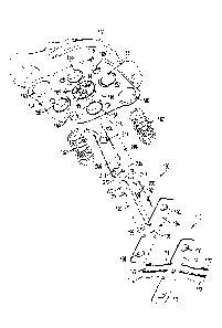
[0071] According to one embodiment, test switch 354 is a two-stage
switch where
upon initial activation, or pressing by a user, contacts "a" and "b" are
electrically
connected. This results in some of the current flowing in line conductors 330,
332 to be
diverted around sense transformer 334 and through resistor 358 to the face
conductors.
By diverting some of the current through resistor 358, an imbalance is caused
in the
current flowing in one direction through conductor 330 and the current flowing
in the
opposite direction through conductor 332. This current imbalance, i.e., net
current, is
detected by circuit 352 and SCR output of GFCI IC 350 is activated.
[0072] When the SCR output is activated it turns ON the gate of SCR 360
allowing
current to flow through fuse 368 and trip coil 362 of solenoid 366. The
current flowing
through trip coil 362 generates a magnetic field that moves an armature within
the
solenoid, e.g., similar to the action of armature 250 within solenoid 108
described above.
When the solenoid armature moves, it unlatches a contact carriage, such as
carriage 106
in the embodiment above, and the carriage drops under the natural bias of the
line
conductors away from the face conductors and the optional load conductors, if
included.
The device is now said to be "tripped," as a result of the successful manual
test sequence,
and the device is ready to be reset. The time it takes from the moment
contacts "a" and
"b" of test switch 354 connect until the device is tripped and current no
longer flows,
particularly through fuse 368 and trip coil 362, is so short that fuse 368
remains intact.
[0073] If, however, the latching mechanism fails to trip and the line
and face (and
possibly load) contacts are not separated when test button 354 is initially
pressed,
continued pressing of switch 354 results in contacts "a" and "b" becoming
disconnected
and contacts "a" and "c" being connected. When this occurs, current flows from
neutral
conductor 332 through resistor 358 and through both coils of solenoid 366,
i.e., fail safe
- 20 -
Date Recue/Date Received 2021-08-13
208273-9011-CA01 (HI 911-0710A CAN)
coil 364 and trip coil 362. Further, some of the current continues to flow
through fuse
368 resulting in its destruction and an open circuit results where fuse 368
was previously.
According to this exemplary embodiment, coils 362 and 364 are concentric and
the
current now flowing through both coils results in a stronger magnetic field
within the
solenoid 366. This stronger magnetic field is generated in a final attempt to
trip the
device and separate the line contacts from the face contacts, that is, the
contacts that
failed to disengage normally when the test button 354 was initially pressed.
MANUAL TESTING VIA THE RESET OPERATION
[0074] With continued reference to FIG. 27, as described above with
respect to the
mechanical aspects of the invention, closing the reset switch 300, e.g., by
pressing reset
button 24 as described with respect to the above embodiments, also initiates a
test
operation. Specifically, when reset switch 300 is closed, a voltage supply
output, VS, of
GFCI IC 350 is electrically connected to the gate of SCR 360 through conductor
308,
thus, turning the SCR ON and drawing current from line conductor 332 through
fuse 368,
trip coil 362 and SCR 360 and ultimately to ground. The current flowing
through coil
362 generates a magnetic field in solenoid 366 and the armature within the
solenoid is
actuated and moves. Under typical, e.g., non-test, conditions the armature is
actuated in
this manner to trip the device, such as when an actual fault or a manual
ground fault via
the test button occurs.
[0075] In this particular situation, however, the device is already in
the tripped
condition, i.e., the line and face (and possibly load) contacts are
electrically isolated. In
this situation the reset button was most likely pressed to re-latch the
contact carriage and
bring the line and face contacts back into electrical contact. This reset
operation is
described in detail above in regard to FIGS. 20-26. For example, the contacts
on reset
switch 300 in FIG. 27 correspond to contacts 172 described above. If the
armature of
solenoid 366 fails to fire, and the reset mechanism, including the contact
carriage
described above, fails to engage the reset plunger on its return after the
reset button is
released, the device will not be reset. Accordingly, if, for example, the
device is not
wired at all, or it is miswired, that is, the device is wired with the AC
power not
- 21 -
Date Recue/Date Received 2021-08-13
208273-9011-CA01 (HI 911-0710A CAN)
connected to the line terminals, e.g., 326, 328, no power is applied to the
GFCI IC 350.
If no power is applied to GFCI IC 350 it cannot drive SCR 360 and the device
will not be
able to be reset, as described above. Thus, the miswire condition is prevented
because
the device cannot be reset until AC power is properly applied to the line
terminals.
THE AUTO-MONITORING CIRCUIT
[0076] With continued reference to the exemplary circuit schematic
shown in FIG.
27, a further aspect of the invention not previously mentioned will now be
described with
respect to auto-monitoring circuit 370. Auto-monitoring circuit 370 includes a
programmable device 301. Programmable device 301 can be any suitable
programmable
device, such as a microcontroller or a microprocessor, which can be programmed
to
implement the auto-monitoring routine as explained in detail below. For
example,
programmable device 301 can be implemented by an ATMELTm microcontroller from
the
ATtiny 10 family or a Microchip microcontroller such as a PIC10F204/206.
[0077] According to one exemplary auto-monitoring, or automatic self-
testing,
routine in accordance with this embodiment, programmable device 301 initiates
the auto-
monitoring routine approximately every three (3) seconds by setting an auto-
monitoring
test flag. The auto-monitoring test flag initiates the auto-monitoring routine
on the circuit
interrupting device and confirms that the device is operating properly or,
under certain
circumstances, determines that the circuit interrupting device has reached its
end-of-life
(EOL). Moreover, this automatic self-testing routine occurs on either half-
cycle of the
AC wave, i.e., either the positive or negative half-cycle. When the auto-
monitoring
routine runs with a positive result, the auto-monitoring circuit enters a
hibernation state
until the programmable device sets the test flag again and initiates another
auto-
monitoring routine.
[0078] If the auto-monitoring routine runs with a negative result,
e.g., it cannot be
determined that the circuit interrupting device is functioning properly, a
failure counter is
incremented and the programmable device initiates another auto-monitoring
routine when
instructed. In addition to the failure count being incremented, a temporary
indication of
the failure can also be provided. For example, a Light Emitting Diode (LED)
may be
- 22 -
Date Recue/Date Received 2021-08-13
208273-9011-CA01 (HI 911-0710A CAN)
flashed one or more times to indicate the failure to a user. If the failure
counter reaches a
predetermined value, i.e., the auto-monitoring routine runs with a negative
result a
predetermined number of times, the auto-monitoring routine invokes an end-of-
life
(EOL) sequence. The EOL sequence then performs one or more of the following
functions; (a) indicates that EOL has been reached, for example, by
continuously flashing
or illuminating an indicator light and/or generating an audible sound, (b)
attempts to trip
the device, (c) prevents an attempt to reset the device, (d) stores the EOL
event on non-
volatile memory, e.g., in the event there is a power failure, and (e) clears
the EOL
condition when the device is powered down.
[0079] In accordance with this embodiment, when the programmable device
determines it is time to run the auto-monitoring routine, a stimulus signal
302 is turned
ON by programmable device 301. When the stimulus signal is turned ON,
electrical
current flows through resistor 303 and transistor 304 is turned ON. When
transistor 304 is
turned ON, current flows from the 3.3V voltage supply through resistor 305,
which is, for
example, a 3k-ohm resistor, and continues through electrical conductor 356 and
transistor
304 to ground. According to this exemplary embodiment, electrical conductor
356 is a
wire connected at one end to resistor 305, traverses through the centers of
sense
transformer 334 and grounded neutral transformer 336 and is looped
approximately six
(6) times around the cores of these transformers and is connected at its other
end to the
collector-emitter of transistor 304. Thus, when the software auto-monitoring
test flag is
set in device 301 and transistor 304 is turned ON, current flows through
conductor 356
which comprises an independent third conductor, e.g., separate from the two,
hot/phase
and neutral, conductors 330 and 332 that also traverse through the centers of
transformers
334 and 336.
[0080] If the circuit interrupting device according to the present
embodiment is
functioning properly, when current flows through third conductor 356, thus
creating a net
current flow through the transformer, a flux is generated at the transformer
which is
detected by detection circuit 352, including GFCI device 350. In accordance
with this
embodiment, when device 350 detects the flux created at 334, a voltage level
is increased
at one of the output ports of device 350, for example at the output port
labeled CAP in
- 23 -
Date Recue/Date Received 2021-08-13
208273-9011-CA01 (HI 911-0710A CAN)
FIG. 27, thus increasing the voltage on line 306. Because conductive line 306
is
connected to a capacitor, 307, the SCR trigger signal 308 of device 350 is
delayed for a
predetermined period of time, i.e., determined by the value of capacitor 307.
For
example, if capacitor 307 is a 1.8 nF capacitor and device 350 is an RV4141
device, SCR
trigger signal 308 is delayed for 3.333 msec. Further, the CAP output, 306, of
device 350
is connected to programmable device 301 via a path that includes conductor 309
and
diode 310 in series with resistor 311, e.g., 4.7 k-Ohm, which completes a
voltage divider
with resistor 312, e.g., 1M-Ohm.
[0081] According to this embodiment, programmable device 301 has an
analog-to-
digital converter (ADC) whose input is connected to conductor 309.
Accordingly, the
ADC of device 301 reads the increasing voltage established on capacitor 307.
When a
predetermined voltage level is reached at the ADC input of programmable device
301,
device 301 turns OFF the auto-monitoring stimulus signal by setting the TST
output to
logic low, thus, turning off transistor 304 and stopping the current flow on
conductor 356
and, thus, the flux created at transformer 334. When this occurs, it is
determined by
programmable device 301 that a qualified auto-monitoring event has
successfully passed
and the auto-monitoring fail counter is decremented if the present count is
greater than
zero.
[0082] In other words, according to this embodiment an auto-monitoring
routine is
repeated by programmable device 301 on a predetermined schedule. For example,
based
on the software program installed within the device, the auto-monitoring
routine is
programmed to be run, as desired, anywhere from every few seconds to every
month, etc.
When the routine is initiated, the flux created at transformer 334 occurs
similarly to the
way a flux would be created if either an actual ground fault had occurred or
if a simulated
ground fault had been manually generated, e.g., by pressing the test button as
described
above. That is, when either an actual or simulated ground fault occurs, a
difference in the
current flowing in the phase and neutral conductors, 330 and 332,
respectively, is created.
This differential, or net, current flowing through sense transformer 334 is
detected by
device 350 which, as a result, drives SCR 360 to turn ON via conductor 308.
When SCR
360 turns ON, current passes through trip coil 362 which trips interrupting
device 315,
- 24 -
Date Recue/Date Received 2021-08-13
208273-9011-CA01 (HI 911-0710A CAN)
i.e., causing the contact carriage to drop, causing the line and face (and
possibly load)
contacts to separate from each other. Thus, current is prevented from flowing
through
phase and neutral conductors 330 and 332 to the phase and neutral face
terminals, 342
and 344, respectively, and the phase and neutral load terminals, 346 and 348,
respectively, when external load terminals are included in the device in
accordance with
the alternative embodiment discussed above.
[0083] In comparison, when the auto-monitoring routine is performed in
accordance
with the present invention, no differential current is created on the phase
and neutral
conductors 330, 332 and the interrupting device 315 is not tripped. Instead,
during the
auto-monitoring routine, the flux generated at sense transformer 334 is a
result of current
flowing through a single, independent third, conductor 356, electrically
isolated from
phase and neutral conductors 334, 336. The current generated on conductor 356
is
present for only a brief period of time, for example, less than the delay time
established
by capacitor 307, discussed previously.
[0084] Thus, if the voltage on conductor 309 and input to the ADC input
of
programmable device 301 reaches a given voltage within this predetermined
period of
time during an auto-monitoring routine, it is determined that the detection
circuit 352
successfully detected the net current flowing in sense transformer 334 and the
auto-
monitoring event has passed. Accordingly, programmable device 301 determines
that
detection circuit 352, including GFCI device 350, is working properly. Because
the net
current flowing through sense transformer 334 during the auto-monitoring
routine is
designed to be substantially similar in magnitude to the differential current
flowing
through the transformer during a simulated ground fault, e.g., 4-6 milliamps,
it is
determined that detection circuit 352 would be able to detect an actual ground
fault and
provide the proper drive signal to SCR 360 to trip interrupter 315.
[0085] Alternatively, the auto-monitoring circuit 370 might determine
that the auto-
monitoring routine has failed. For example, if it takes longer than the
predetermined
period of time for the voltage at the ADC input of programmable device 301 to
reach the
given voltage during the auto-monitoring routine, it is determined that the
auto-
monitoring event failed. If this occurs, an auto-monitoring fail tally is
incremented and
- 25 -
Date Recue/Date Received 2021-08-13
208273-9011-CA01 (HI 911-0710A CAN)
the failure is indicated either visually or audibly. For example, according to
one
embodiment, the ADC port of programmable device 301 is converted to an output
port
when an auto-monitoring event failure occurs and a voltage is placed on
conductor 309
via the converted I/O port, generating a current to flow on conductor 309,
through
indicator LED 316 and resistor 317 to ground. Subsequently, the ADC I/O port
of
programmable device 301 is converted back to an input for the next scheduled
auto-
monitoring event.
[0086] For example, when an auto-monitoring event failure occurs,
indicator LED
316 illuminates only for the period of time when the I/O port is converted to
an output
and an output voltage is generated at that port; otherwise LED 316 remains
dark, or non-
illuminated. Thus, if the auto-monitoring routine is run, for example, every
three (3)
seconds, and an event failure occurs only a single time or sporadically, the
event is likely
to go unnoticed by the user. If, on the other hand, the failure occurs
regularly, as would
be the case if one or more of the components used in the auto-monitoring
routine is
permanently disabled, the indicator LED 316 would blink at a regular interval,
thus
drawing attention to the device and informing the user that critical
functionality of the
device has been compromised. Conditions that cause the auto-monitoring routine
to fail
include one or more of the following, open circuited differential transformer,
closed
circuited differential transformer, no power to the GFCI IC, open circuited
solenoid, SCR
trigger output of the GFCI IC continuously high, and SCR output of the GFCI IC
continuously low.
[0087] According to a further aspect of this embodiment, if the auto-
monitoring fail
tally reaches a predetermined limit, for example, seven (7) failures within
one (1) minute,
programmable device 301 enters an end-of-life (EOL) state. If this occurs, an
audible or
visual indicator is activated to alert the user that the circuit interrupting
device has
reached the end of its useful life. For example, when an EOL state is
determined, the
ADC I/O port of programmable device 301 is converted to an output port,
similar to
when a single failure is recorded as described above, and a signal is either
periodically
placed on conductor 309 via the ADC output port, i.e., to blink LED 316, or a
signal is
- 26 -
Date Recue/Date Received 2021-08-13
208273-9011-CA01 (HI 911-0710A CAN)
continuously placed on conductor 309 to permanently illuminate LED 316. The
auto-
monitoring routine is also halted at this time.
[0088] Additionally, according to a further embodiment, when EOL is
determined,
programmable device 301 attempts to trip interrupting device 315 in one or
both of the
following ways: (a) by maintaining the stimulus signal on third conductor 356
into the
firing half-cycle of the AC wave, and/or, (b) by converting the EOL port of
programmable device 301 to an output, if it is currently an input port, and
placing a drive
signal on conductor 318 to directly drive the gate of SCR 320 to turn SCR 320
ON, thus,
enabling it to conduct current and activate the solenoid. More specifically,
when SCR
320 is turned ON, current is drawn through fail safe coil 364 of dual coil
solenoid 366.
For example, dual coil solenoid 366 includes inner fail safe coil 364, which
comprises a
300 turn, 10 Ohm, coil, and outer main, trip, coil 362, which comprises an 880
turn, 25.5
Ohm, coil.
[0089] Accordingly, when it is determined via the auto-monitoring
routine that
detection circuit 352 is not successfully detecting ground faults, e.g., it
does not detect the
flux resulting from current flowing in conductor 356, or that it is not
otherwise generating
a drive signal on conductor 308 to drive SCR 360 upon such detection,
programmable
device 301 determines EOL and attempts to trip interrupting device 315 by one
or both of
two separate methods. Specifically, device 301 attempts to directly trip
interrupting
device 315 by either, (a) continuing to generate the signal on conductor 356,
or, (b)
directly driving the fail safe coil 364, or, both, (a) and (b). There is one
significant
difference, however, between the signal on conductor 356 when the auto-
monitoring
routine is being run normally, and the signal on conductor 356 that is
generated when
EOL is determined. That is, under EOL conditions, the signal, e.g., electrical
pulse, on
conductor 356 is extended into, or otherwise generated in, the firing half-
cycle of the AC
wave. This should generate flux at transformer 334 which, assuming all else is
working
properly, causes SCR 360 to be triggered and trip coil 362 to be energized,
thus
activating the solenoid to trip the interrupting device 315.
[0090] When the second method (b) above, is employed, that is, SCR 320
is driven to
draw current through fail safe coil 364 to trip interrupting device 315, the
current is first
- 27 -
Date Recue/Date Received 2021-08-13
208273-9011-CA01 (HI 911-0710A CAN)
drawn through fuse 368, which may comprise a regular fuse, a fusible resistor
or any
other fusible element, such as a drip of solder. If interrupting device 315
fails to open
and, in particular, open in a very short amount of time, the current being
drawn through
fuse 368 will destroy the fuse, i.e., cause an open-circuit, and the current
will no longer
flow, leaving no further opportunities for the programmable device 301 to trip
interrupting device 315.
[0091] If both methods (a) and (b) above are employed for tripping
interrupting
device 315 in the event of an EOL condition, both coils, 362, 364 of dual coil
solenoid
366 are energized. Further, if either of the two methods, (a) and (b),
successfully opens
interrupting device 315, or if interrupting device was otherwise already open,
power-on
indicator circuit 321 will be OFF. For example, in the embodiment shown in
FIG. 27,
power on indicator circuit includes LED 322 in series with resistor 323 and
diode 324.
One lead of LED 322 is connected to the neutral face terminal 344 and one lead
of diode
324 is connected to phase face terminal 342. Accordingly, when power is
available at the
face terminals, current is drawn through the power on circuit on each
alternating half-
cycle of AC power, thus, making LED 322 blink. If, on the other hand, power is
not
available at the face terminals 342, 344, for example, because interrupting
device 315 is
open, or tripped, then LED 322 will be dark, or not illuminated.
[0092] Additional embodiments and aspects thereof, related to the auto-
monitoring
functionality consistent with the present invention, as well as further
discussion of some
of the aspects already described, are provided below.
[0093] For example, the sinusoidal AC waveform includes two half-
cycles, a positive
half-cycle and a negative half-cycle. The so-called firing half-cycle refers
to the
particular half-cycle, either positive or negative, during which a gate
trigger signal to an
SCR, for example SCR 360 and/or SCR 320, results in the respective solenoid
coil
conducting current and the solenoid firing, e.g., where the armature moves. A
non-firing
half-cycle refers to the alternate half-cycle of the AC waveform, i.e., either
negative or
positive, where current does not flow through an SCR or its respective
solenoid coil,
regardless of whether or not the SCR gate is triggered. Whether the positive
or negative
- 28 -
Date Recue/Date Received 2021-08-13
208273-9011-CA01 (HI 911-0710A CAN)
half-cycle is the firing half-cycle is typically determined by a diode placed
in series with
the respective solenoid coil.
[0094] Under optimal conditions the auto-monitoring routine consistent
with
embodiments of the invention can be performed at any time within a given AC
cycle, that
is, during either the positive or negative (firing or non-firing) half-cycle.
Of course, it
would be ideal if the auto-monitoring routine could be completed entirely
during the non-
firing half-cycle, so that any unintentional firing of the solenoid, for
example, due to
inadvertent SCR triggering, is avoided. Such an ideal situation may not be
possible,
however, due to, for example, inadequate voltage sampling times by the
programmable
device, how the circuit is configured, and/or how the GFCI device is powered.
[0095] One unfavorable scenario occurs when the auto-monitoring routine
is
performed only during the firing half-cycle of the solenoid. Accordingly, the
programmable device according to at least one exemplary embodiment of the
present
invention is able to turn ON the test current, e.g., on independent, third,
line 356, sample
a voltage level, e.g., at the ADC input of device 301, make a determination
whether the
routine has passed, and then turn OFF the test current, all within a very
small time period
so as not to trigger the SCR during a firing half-cycle. The auto-monitoring
circuit
according to this embodiment, e.g., circuit 370, operates in this condition
and as such one
auto-monitoring event is completed within 250 microseconds.
[0096] According to a further embodiment of a circuit interrupting
device consistent
with the invention, programmable device 301 also can optionally monitor the AC
power
input to the device. For example, the device can monitor the 60 Hz AC input
that is
electrically connected to the phase and neutral line terminals 326, 328.
[0097] A full AC cycle at 60 Hz takes approximately 16.333 milliseconds
to
complete. Thus, to monitor and confirm receipt and stabilization of the AC
waveform, a
timer/counter within programmable device 301 is implemented. For example,
within a
100 millisecond window there should be at least 6 positive transitions of a 60
Hz signal.
However, because AC frequencies may fluctuate at 60 Hz, the qualifying event
count,
e.g., to determine that AC power has been applied to the device, is set to
less than 6 such
transitions, for example, 3 positive transitions. Accordingly, the situation
is
- 29 -
Date Recue/Date Received 2021-08-13
208273-9011-CA01 (HI 911-0710A CAN)
accommodated where a circuit interrupting device in accordance with the
invention is
connected to a variable power source, such as a portable generator, that
exhibits a lower
frequency at start-up and requires a stabilization period before the optimal
frequency,
e.g., 60 Hz, is achieved.
[0098] Further, to confirm that the applied AC power waveform has
stabilized at the
optimal frequency, programmable device 301 counts the number of positive
transitions
repetitively occurring within a given period, for example 6 transitions within
a 100
millisecond period. If the frequency is not stabilized at the optimal
frequency, or at least
not within an acceptable range, the initiation of the auto-monitoring routine
is delayed
until the frequency is stabilized. If the frequency does not achieve the
optimal frequency,
or a frequency within an acceptable range, within a predetermined time, a fail
tally is
incremented. Similar to the fail tally discussed previously with respect to
the auto-
monitoring routine, if the tally reaches a given threshold, the programmable
device 301
can declare EOL.
[0099] As described above, according to at least one exemplary
embodiment,
programmable device 301 is implemented in a microprocessor. Because some
microprocessors include non-volatile memory, e.g., for storing various data,
etc., in the
event of a power outage, according to a further embodiment all events, timers,
tallies
and/or states within the non-volatile memory are cleared upon power-up of the
device.
Accordingly, if the fail tally or other condition resulted from improper
device installation,
inadequate or improper power, or some other non-fatal condition with respect
to the
circuit interrupting device itself, the fail tally would be reset on power-up,
when the tally
incrementing event may no longer be preset. Of course, another way of avoiding
this
potential issue is to utilize a programmable device that does not have non-
volatile
memory.
[00100] While various embodiments have been chosen to illustrate the
invention, it
will be understood by those skilled in the art that other modifications may be
made
without departing from the scope of the invention as defined by the appended
claims.
Several possible modifications are mentioned below by way of example only.
- 30 -
Date Recue/Date Received 2021-08-13
208273-9011-CA01 (HI 911-0710A CAN)
[00101] The reset switch may take forms other than two contact pads 144 on the
circuit board and a bridging contact 172 on the carriage. For example, the
reset switch
could comprise a single contact on the circuit board closable with a single
contact on the
underside of the carriage, which could be connected to another part of the
circuit by a
flexible jumper wire. Alternatively, the reset switch could be a self-
contained momentary
switch mounted on or beneath the circuit board and having a protruding stem
that would
be depressed by the carriage near the end of its downward travel. Another
alternative
could be a proximity switch mounted on the circuit board that would close when
the
carriage comes within triggering range of the switch.
[00102] The latching mechanism could take forms other than a shouldered collar
241
on the reset plunger and resilient, shouldered latch beams 192 and reset beams
206 on the
carriage. For example, shouldered resilient beams or their equivalents could
be located
on the reset plunger and mating fixed shoulders could be located on the
carriage latching
portion, with the armature modified to retract the resilient beams as it moves
downward.
Alternatively, the reset plunger could be made hollow so that the armature
moves within
it to retract plunger-mounted latching elements, rather than vice versa. Other
suitable
variations will be apparent to those skilled in the art.
-31 -
Date Recue/Date Received 2021-08-13