Note: Descriptions are shown in the official language in which they were submitted.
PHOTODIODE AND METHOD FOR MAKING THE SAME
BACKGROUND
This application relates to photovoltaic devices and, more particularly, to
photodiodes formed with quantum nanomaterials and, even more particularly, to
photodiodes fonned with quantum nanomaterials using solution processing
techniques.
Photodiodes convert the sun's energy into useful electrical energy (current or
voltage) by way of the photovoltaic effect. Modem photodiodes are relatively
lightweight and they operate at relatively high efficiencies. Therefore,
photodiodes
provide a reliable, lightweight and sustainable source of electrical energy
suitable for a
variety of applications, including terrestrial and space applications.
Photodiodes are typically fabricated using vacuum deposition techniques to
grow
thin layers of semiconductor material on a substrate. The resulting
photodiodes may then
be electrically interconnected in large arrays to harvest the sun's energy and
produce
useful electrical energy.
Unfortunately, vacuum deposition techniques generally require a substrate
having
a relatively small surface area (less than 1 ft2) for proper growth and,
therefore, are not
suitable for large surface area applications. Furthermore, vacuum deposition
techniques
are generally not suitable for curved surfaces and, therefore, are limited to
relatively
small, flat substrates. Still furthermore, vacuum deposition techniques are
relatively
expensive and, therefore, significantly contribute to the overall cost of
photodiodes.
Accordingly, those skilled in the art continue with research and development
efforts in the field of lightweight, high efficiency photodiodes, including
the fabrication
of lightweight, high efficiency photodiodes.
SUMMARY
In one embodiment, disclosed is a method for manufacturing a photodiode. The
method may include the steps of providing a substrate, solution depositing
(e.g., spin
coating) a quantum nanomaterial layer onto the substrate, the quantum
nanomaterial layer
including quantum nanomaterials having a ligand coating, and applying a thin-
film oxide
layer over the quantum nanomaterial layer.
¨1 ¨
Date Recue/Date Received 2023-02-13
In another embodiment, the disclosed method may include the steps of providing
a
substrate, solution depositing (e.g., spin coating) a quantum nanomaterial
layer onto the
substrate, the quantum nanomaterial layer including quantum nanomaterials
having a
ligand coating, and solution depositing (e.g., spin coating) a thin-film oxide
layer over the
quantum nanomaterial layer.
In another embodiment, the disclosed method may include the steps of providing
a
substrate, forming bottom contacts on the substrate, solution depositing
(e.g., spin
coating) a quantum nanomaterial layer onto the substrate, the quantum
nanomaterial layer
including quantum nanomaterials (e.g., tin-telluride and/or lead-tin-
telluride) having a
ligand coating (e.g., a metal halide ligand and/or a metal chalcogenide
complex), applying
a thin-film oxide layer over the quantum nanomaterial layer, and forming top
contacts on
the thin-film oxide layer.
In another embodiment, the disclosed photodiode may include a substrate, a
solution-cast quantum nanomaterial layer positioned on the substrate, the
solution-cast
quantum nanomaterial layer including tin-telluride quantum nanomaterials
having a
ligand coating, wherein the ligand coating includes a metal halide ligand
and/or a metal
chalcogenide complex, wherein the metal chalcogenide complex includes tin
and/or a
transition metal, and a thin-film oxide layer over the solution-cast quantum
nanomaterial
layer.
In yet another embodiment, the disclosed photodiode may include a substrate, a
solution-cast quantum nanomaterial layer positioned on the substrate, the
solution-cast
quantum nanomaterial layer including lead-tin-telluride quantum nanomaterials
having a
ligand coating, wherein the ligand coating includes a metal halide ligand
and/or a metal
chalcogenide complex, wherein the metal chalcogenide complex includes tin
and/or a
transition metal, and a thin-film oxide layer over the solution-cast quantum
nanomaterial
layer.
In the text and the figures, a method is disclosed for manufacturing a
photodiode
including the steps of providing a substrate, solution depositing a quantum
nanomaterial
layer onto said substrate, said quantum nanomaterial layer comprising a
plurality of
quantum nanomaterials, each quantum nanomaterial of said plurality including a
ligand
coating, and applying a thin-film oxide layer over said quantum nanomaterial
layer.
Alternatively, the method may include wherein said substrate includes a
semiconductor material.
¨ 2 ¨
Date Recue/Date Received 2023-02-13
Alternatively, the method may include wherein said semiconductor material
includes germanium.
Alternatively, the method may include wherein said germanium is doped p-type
germanium.
Alternatively, the method may further include the step of sulfur passivating
said
substrate prior to said solution depositing step.
Alternatively, the method may include wherein said substrate comprises at
least
one of a metal foil and a polymeric film.
Alternatively, the method may include wherein said plurality of quantum
nanomaterials is a plurality of quantum dots, and wherein each quantum dot of
said
plurality of quantum dots comprises at least one of tin-telluride and lead-tin-
telluride.
Alternatively, the method may include wherein said plurality of quantum
nanomaterials comprise tin-telluride.
Alternatively, the method may include wherein said plurality of quantum
nanomaterials have maximum cross-sectional dimension between about 15
nanometers
and about 50 nanometers.
Alternatively, the method may include wherein said plurality of quantum
nanomaterials comprise lead-tin-telluride.
Alternatively, the method may include wherein said plurality of quantum
nanomaterials have maximum cross-sectional dimension of at least about 7.5
milometers.
Alternatively, the method may include wherein said ligand coating comprises a
metal chalcogenide complex, wherein said metal chalcogenide complex comprises
at least
one of tin and a transition metal.
Alternatively, the method may include wherein said ligand coating comprises at
least one of tin-sulfide, tin-selenide and tin-telluride.
Alternatively, the method may include wherein said ligand coating comprises a
metal halide ligand.
Alternatively, the method may include wherein said thin-film oxide layer is
applied by a solution deposition process.
Alternatively, the method may include wherein said thin-film oxide layer
comprises an amorphous oxide semiconductor.
Alternatively, the method may further include the step of applying a first
contact layer
over said thin-film oxide layer.
¨ 3 ¨
Date Recue/Date Received 2023-02-13
Alternatively, the method may further include the step of applying a second
contact
layer onto said substrate.
In another aspect, a photodiode is disclosed including: a substrate, a
solution-cast
quantum nanomaterial layer positioned on said substrate, said solution-cast
quantum
.. nanomaterial layer comprising tin-telluride quantum nanomaterials
comprising a ligand
coating, wherein said ligand coating includes at least one of a metal halide
ligand and a metal
chalcogenide complex, wherein said metal chalcogenide complex includes at
least one of tin
and a transition metal, and a thin-film oxide layer over said solution-cast
quantum
nanomaterial layer.
In another aspect, a photodiode is disclosed including: a substrate, a
solution-cast
quantum nanomaterial layer positioned on said substrate, said solution-cast
quantum
nanomaterial layer comprising lead-tin-telluride quantum nanomaterials
comprising a ligand
coating, wherein said ligand coating comprises at least one of a metal halide
ligand and a
metal chalcogenide complex, wherein said metal chalcogenide complex includes
at least one
of tin and a transition metal, and a thin-film oxide layer over said solution-
cast quantum
nanomaterial layer.
In another embodiment, the disclosed method for manufacturing a photodiode may
comprise steps of: providing a substrate comprising germanium; doping said
substrate;
subjecting said substrate to sulfur passivation; cleaning said substrate after
said sulfur
passivation; solution depositing a quantum nanomaterial layer onto said
substrate, said
quantum nanomaterial layer comprising a plurality of quantum nanomaterials,
each quantum
nanomaterial of said plurality comprising: a core comprising at least one of
tin-telluride and
lead-tin-telluride which is tuned to absorb radiation within a bandwidth of
mid-wavelength
infrared and long-wavelength infrared; and a ligand coating on said core
comprising a metal
chalcogenide complex comprising at least one of tin-sulfide, tin-selenide and
tin-telluride,
wherein said ligand coating is applied to said core using a ligand exchange
reaction to
substitute an original coating on said core; and applying a thin-film oxide
layer over said
quantum nanomaterial layer.
In another embodiment, the disclosed method for manufacturing a photodiode may
comprise steps of: providing a substrate comprising germanium; doping said
substrate;
subjecting said substrate to sulfur passivation; cleaning said substrate after
said sulfur
passivation; solution depositing a quantum nanomaterial layer onto said
substrate, said
quantum nanomaterial layer comprising a plurality of quantum dots, each
quantum dot of said
¨ 4 ¨
Date Recue/Date Received 2023-02-13
plurality comprising: a core comprising at least one of tin-telluride and lead-
tin-telluride
which is tuned to absorb radiation within a bandwidth of mid-wavelength
infrared and long-
wavelength infrared; and a ligand coating on said core comprising at least one
of tin-sulfide,
tin-selenide and tin-telluride, wherein said ligand coating is applied to said
core using a
ligand exchange reaction to substitute an original coating on said core; and
solution
depositing a thin-film oxide layer over said quantum nanomaterial layer.
In another embodiment, the disclosed photodiode may comprise: a substrate
comprising doped germanium and a sulfur-passivated surface; a solution-cast
quantum
nanomaterial layer positioned on said sulfur-passivated surface of said
substrate, said
solution-cast quantum nanomaterial layer comprising a plurality of quantum
nanomaterials
tuned to absorb radiation within a bandwidth of mid-wavelength infrared and
long-
wavelength infrared, each quantum nanomaterial of said plurality of quantum
nanomaterials
comprising: a core comprising tin-telluride; a ligand coating on said core,
said ligand coating
comprising a metal chakogenide complex, comprising at least one of tin-
sulfide, tin-selenide
and tin-telluride; and a thin-film oxide layer over said solution-cast quantum
nanomaterial
layer.
In another embodiment, the disclosed photodiode may comprise: a substrate
comprising doped germanium and a sulfur-passivated surface; a solution-cast
quantum
nanomaterial layer positioned on said sulfur-passivated surface of said
substrate, said
solution-cast quantum nanomaterial layer comprising a plurality of quantum
nanomaterials
tuned to absorb radiation within a bandwidth of mid-wavelength infrared and
long-
wavelength infrared, each quantum nanomaterial of said plurality of quantum
nanomaterials
comprising: a core comprising lead-tin-telluride; and a ligand coating on said
core, said
ligand coating comprising a metal chalcogenide complex, comprising at least
one of tin-
sulfide, tin-selenide and tin-telluride; and a thin-film oxide layer over said
solution-cast
quantum nanomaterial layer.
Other embodiments of the disclosed photodiode and method for making the same
will
become apparent from the following detailed description, the accompanying
drawings and the
appended claims.
- 5 ¨
Date Recue/Date Received 2021-08-20
BRIEF DESCRIPTION OF THE DRAWINGS
Fig. 1 is a schematic side elevational view, in section, of one embodiment of
the
disclosed photodiode;
Fig. 2 is a flow chart illustrating one embodiment of the disclosed method for
making
a photodiode; and
Figs. 3A and 3B are graphical illustrations of the current-voltage
characteristics of
one example of the disclosed photodiode, shown prior to being illuminated
(Fig. 3A) and
while being illuminated (Fig. 3B).
DETAILED DESCRIPTION
It has now been discovered that photodiodes may be manufactured using solution
deposition techniques, such as spin coating, stamping or printing. The
disclosed solution
deposition techniques may be used to manufacture photodiodes configured to
operate within a
particular wavelength range (e.g., long wave infrared) at a relatively lower
cost than using
traditional vapor deposition techniques. Furthermore, the disclosed solution
deposition
techniques may be used for large surface area (> 1 ft2) applications, and may
be used on flat,
as well as curved, surfaces.
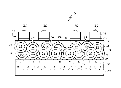
Referring to Fig. 1, one embodiment of the disclosed photodiode, generally
designated 10, may include a substrate layer 12, a quantum nanomaterial layer
14 and a thin-
film oxide layer 16. A first contact layer 18 may be applied over the thin-
film oxide layer 16.
Optionally, a second contact layer 20 may be applied over the substrate layer
12.
The substrate layer 12 may provide the surface upon which the quantum
nanomaterial
layer 14 may be deposited. Those skilled in the art will appreciate that
various materials (or
combination of materials) may be used to form the substrate layer 12 without
departing from
the scope of the present disclosure.
In a first variation, the substrate layer 12 may be formed from a
semiconductor
material. For example, the substrate layer 12 may be founed from germanium,
such as
germanium that starts as p-type germanium or germanium that has been doped p-
type
germanium. However, various semiconductor substrate materials may be used to
form the
substrate layer 12, and the semiconductor substrate materials may optionally
be doped to
achieve the desired electrical properties.
Optionally, the semiconductor substrate material (e.g., germanium) may be
subjected
to sulfur passivation (S-passivation). While various sulfur passivation
techniques may be
used, one suitable example includes aqueous (NH4)25 treatment, as described in
greater detail
¨ 6 ¨
Date Recue/Date Received 2021-08-20
in Thathachary AN. et al., "Fermi Level Depinning at the Germanium Schottky
Interface
Through Sulfur Passivation," App!. Phy. Lett. 96, 152108 (2010). Without being
limited to
any particular theory, it is believed that sulfur passivation of the
semiconductor substrate
material may de-pin the Fermi level at the surface of the semiconductor
substrate material to
make repeatable ohmic contacts to the semiconductor substrate.
In a second variation, the substrate layer 12 may be formed from a non-
semiconductor
material. Various non-semiconductor materials, such conductive materials, non-
conductive
materials, flexible materials and rigid materials, are contemplated. The non-
semiconductor
materials may be coated with various materials, such as conductors and/or
insulators, to
achieve the desired electrical properties.
In one expression of the second variation, the substrate layer 12 may include
a
conductive, flexible foil, such as a metal foil. The conductive, flexible foil
may be coated
with a thin layer (e.g., 25 nanometers or less) of insulator. As one example,
the insulator
may be applied using a solution process, such as solution-processed
aluminophosphate or
solution-processed hafnium oxysulfate. As another example, the insulator may
be applied
using a physical vapor deposition process. Without being limited to any
particular theory,
it is believed that the insulator may allow carriers to tunnel through to the
underlying
conductive, flexible foil, but may preclude direct contact between the quantum
nanomaterial layer 14 and the conductive, flexible foil, which may quench the
desired
properties of the quantum nanomaterials in the quantum nanomaterial layer 14.
In another expression of the second variation, the substrate layer 12 may
include a
non-conductive polymeric film, such as polyetheretherketone. The non-
conductive
polymeric film may be coated with a thin, highly conductive layer. For
example, the thin,
highly conductive layer may be a thin metal (e.g., silver) layer applied using
a physical
vapor deposition process. Then, the thin, highly conductive layer may be
coated with a
thin layer (e.g., 25 nanometers or less) of insulator, such as by using a
solution process or
a physical vapor deposition process, as described above.
The quantum nanomaterial layer 14 may include a plurality of quantum
nanomaterials 22 applied onto a surface 13 of the substrate layer 12 as a thin
film using a
solution deposition technique. Examples of suitable solution deposition
techniques
include spin coating, stamping and printing.
The quantum nanomaterials 22 may be quantum dots, quantum rods, nano-
tetrapods or any other nanocrystalline semiconductor material. As one specific
example,
the quantum nanomaterials 22 may be tin-telluride (SnTe) quantum dots. As
another
¨ 7 ¨
Date Recue/Date Received 2021-08-20
specific example, the quantum nanomaterials 22 may be lead-tin-telluride
(Plz(i-x)SnxTe,
where x is a number between 0.1 and 0.6) quantum dots.
The quantum nanomaterials 22 may be tuned to absorb infrared radiation, such
as infrared
radiation within the bandwidth of mid-wavelength infrared (3-5 micrometers)
and long-
wavelength infrared (5-15 micrometers). Tuning the quantum nanomaterials 22 to
absorb
infrared radiation within the mid-wavelength and long-wavelength infrared
spectrum may
require specific material selection (e.g., forming the quantum nanomaterials
22 to a
particular size, as described in greater detail in U.S. Patent App. No.
13/022,705
("Nanomaterial Having Tunable Infrared Absorption Characteristics and
Associated Method
of Manufacture") filed on February 8, 2011. As one example, the quantum
nanomaterials 22
may be formed from tin-telluride (SnTe) and may have a maximum cross-sectional
dimension
of between about 15 and about 50 nanometers. As another example, the quantum
nanomaterials 22 may be formed from lead-tin-telluride (PbõSn(l,)Te, where x
is a number
between 0.1 and 0.6) and may have a maximum cross-sectional dimension of at
least about
7.5 nanometers.
The quantum nanomaterials 22 may include a ligand coating 24. The ligand
coating
24 may include an inorganic ligand or a combination of inorganic ligands. The
use of organic
ligands is also contemplated. Without being limited to any particular theory,
it is believed
that the ligand coating 24 may bind-up bonds on the surface of the quantum
nanomaterials 22,
and may allow closer spacing between adjacent quantum nanomaterials 22 within
the
quantum nanomaterial layer 14.
In one formulation, the ligand coating 24 may include a metal chakogenide
complex
("MCC"). The metal chalcogenide complex may include a metal and a chalcogen,
such as
sulfur, selenium or tellurium, wherein the metal includes either tin and/or a
transition metal.
Examples of metal chakogenide complexes suitable for use as the ligand coating
24 include
tin-sulfide (SnS), tin-selenide (SnSe) and tin-telluride SnTe.
In another formulation, the ligand coating 24 may include a metal halide
ligand. For
example, the halide may be iodide, bromide and/or chloride. An example of a
metal halide
ligand suitable for use as the ligand coating 24 is titanium chloride (TiO4).
The ligand coating 24 may be applied to the quantum nanomaterials 22 using a
ligand
exchange process. The process of manufacturing quantum nanomaterials 22 may
result in
quantum nanomaterials 22 having a coating (e.g., oleic acid) already on the
surface thereof
The ligand exchange process may substitute the original coating (e.g., oleic
acid) for the
desired ligand coating 24 (e.g., SnS, SnSe or SnTe).
¨ 8 ¨
Date Recue/Date Received 2021-08-20
As one non-limiting example, a dispersion of quantum nanomaterials 22 having a
ligand coating 24 suitable for forming the quantum nanomaterial layer 14 may
be prepared as
follows. First, tin-telluride (SnTe) nanocrystals may be manufactured as
described in U.S.
Patent App. No. 13/022,705. The manufacturing process may be controlled such
that the
resulting tin-telluride nanocrystals are tuned to the desired wavelength
(e.g., long-wavelength
infrared). The tin-telluride nanocrystals may have an oleic acid coating, and
may be
dispersed in hexane. Second, a ligand exchange reaction may be performed to
coat the
tin-telluride nanocrystals with a tin-sulfide (SnS) metal chalcogenide
complex. Finally,
the SnS-coated tin-telluride nanocrystals may be dispersed in hydrazine.
To form the quantum nanomaterial layer 14, the dispersion of SnS-coated tin-
telluride nanocrystals in hydrazine may be solution deposited onto the
substrate layer 14,
such as by spin coating, stamping or printing. The solution deposition process
(e.g., spin
coating) may continue until the desired cross-sectional thickness of the
quantum
nanomaterial layer 14 is achieved. Then, after solution deposition, the
resulting layered
structure may be heat-treated (e.g., 60 minutes at 280 C).
The thin-film oxide layer 16 may be applied over the quantum nanomaterial
layer
14, and may optionally infiltrate the quantum nanomaterial layer 14. The thin-
film oxide
layer 16 may be electrically conductive, and may be generally transparent to
the
electromagnetic radiation intended to be absorbed by the quantum nanomaterial
layer 14.
The thin-film oxide layer 16 may be fonned from an amorphous oxide
semiconductor. Those skilled in the art will appreciate that various amorphous
oxide
semiconductors may be used to form the thin-film oxide layer 16. Two specific
examples
of amorphous oxide semiconductors suitable for forming the thin-film oxide
layer 16 are
zinc-tin-oxide (ZTO) and indium-gallium-zinc-oxide (IGZO).
In one construction, the thin-film oxide layer 16 may be formed using a
solution
deposition process. For example, the thin-film oxide layer 16 may be formed by
synthesizing indium-gallium-zinc-oxide (IGZO) using a solution deposition
process. A
suitable IGZO solution was obtained from Inpria Corporation of Corvallis,
Oregon. The
resulting solution deposited thin-film oxide layer 16 may be heat treated for
60 minutes at
300 C.
In another construction, the thin-film oxide layer 16 may be formed using a
physical vapor deposition process. For example, the thin-film oxide layer 16
may be
formed from zinc-tin-oxide (ZTO) using vacuum deposition.
- 9 ¨
Date Recue/Date Received 2021-08-20
Thus, the quantum nanomaterial layer 14 may be positioned between the
substrate
layer 12 and the thin-film oxide layer 16. Additional layers may be
incorporated into the
photodiode 10 without departing from the scope of the present disclosure.
The first contact layer 18 may be applied over the thin-film oxide layer 16
and
-- may be electrically coupled to the thin-film oxide layer 16. The first
contact layer 18 may
be formed from a conductive metal 28, such as gold, platinum, nickel, aluminum
and/or
tantalum. An optional tie layer 26, such as titanium, may be positioned
between the
conductive metal 28 of the first contact layer 18 and the thin-film oxide
layer 16 to
enhance bonding between the conductive metal 28 and the underlying thin-film
oxide
.. layer 16.
The first contact layer 18 may be applied to the thin-film oxide layer 16 in
various
patterns (e.g., a grid pattern) using various techniques. As one example, the
first contact
layer 18 may be applied using a stamping process. As another example, the
first contact
layer 18 may be applied using a physical vapor deposition process (evaporation
or
-- sputtering), wherein lithography may be used to defme the pattern of the
first contact
layer 18.
Optionally, indium bumps 30 may be applied to (e.g., evaporated onto) the
first
contact layer 18.
The second contact layer 20 may optionally be applied over the substrate layer
12
and may be electrically coupled to the substrate layer 12. The second contact
layer 20
may be formed from a conductive metal, such as gold, platinum, nickel,
aluminum and/or
tantalum_
Also disclosed is a method for manufacturing a photodiode. Referring to Fig.
2,
one embodiment of the disclosed method for manufacturing a photodiode,
generally
designated 100, may begin at Block 102 with the step of providing a substrate.
For
example, the substrate provide at Block 102 may be germanium.
At Block 104, the substrate may be treated. As one treatment, the substrate
may
be doped. For example, the germanium substrate may be doped with p-type
dopants to
achieve a charge carrier density of about 1013. As another treatment, the
substrate may be
subjected to sulfur passivation. For example, the p-doped germanium substrate
may be
passivated in a (N114)2S solution for 30 minutes with a resistivity of 24.5 to
27.5 ohms/sq.
After sulfur passivation, the substrate may be: (1) cleaned in an HCL/HBr
solution for
five minutes; (2) rinsed with de-ionized water for 5 minutes and blown dry
with N2; (3)
-10 ¨
Date Recue/Date Received 2021-08-20
treated with a 40% aqueous ammonium sulfide solution at 50 C for 5 minutes;
then (4)
rinsed with de-ionized water for 5 minutes and blown dry with N2.
At Block 106, the bottom contacts may be applied to the substrate. For
example,
the bottom contacts may be applied as follows: (1) lithography may be
performed on the
germanium substrate; (2) a metal, such as gold, platinum, nickel, aluminum
and/or
tantalum, may be applied (e.g., sputtered) over the lithography; and (3) the
lithography
may be lifted-off to define the bottom contacts. Optionally, AMD may be
performed,
followed by a di-ionized water rinse for 5 minutes, followed by ozone
treatment for 10 to
30 minutes.
At Block 108, a quantum nanomaterial layer may be applied to the substrate
using
a solution deposition technique, such as spin coating, stamping or printing.
For example,
the dispersion of SnS-coated tin-telluride nanocrystals in hydrazine may be
applied to the
germanium substrate by spin coating to achieve the desired thickness. The SnS-
coated
tin-telluride nanocrystal layer (on the germanium substrate) may be heat
treated for 60
minutes at 280 C, as shown at Block 110.
At Block 112, a thin-film oxide layer may be applied over the quantum
nanomaterial layer. For example, an indium-gallium-zinc-oxide (IGZO) solution
available from Inpria Corporation of Corvallis, Oregon, may be applied to the
SnS-coated
tin-telluride nanocrystal layer by spin coating to achieve the desired
thickness (e.g., a
single layer about 20 to 25 nanometers thick). The IGZO thin-film oxide layer
(on the
quantum nanomaterial layer, which is on the germanium substrate) may be heat
treated
for 60 minutes at 300 C, as shown at Block 114. As another example, the thin-
film
oxide layer (e.g., zinc-tin-oxide) may be applied over the quantum
nanomaterial layer
using a traditional physical vapor deposition (PVD) process or poly inorganic
condensation (PIC) process, which may not require an additional, post-
deposition heat
treatment step.
Optionally, an ozone treatment step may be performed following formation of
the
thin-film oxide layer (e.g., after Block 114).
At Block 116, the top contacts may be applied to the thin-film oxide layer.
For
example, the top contacts may be applied as follows: (1) photolithography may
be
performed on the thin-film oxide layer to define the top contacts; (2) a
metal, such as gold
with an optional titanium tie layer, may be applied (e.g., sputtered) over the
photolithography; and (3) the photolithography may be lifted-off to define the
top
contacts.
-11-
Date Recue/Date Received 2021-08-20
Optionally, an indium bumps application step may be performed following
formation of the top contacts (e.g., after Block 116).
Figs 3A and 3B show the current-voltage characteristics of a photodiode
manufactured in accordance with the disclosed method 100 on a sulfur
passivated, p-type
doped germanium substrate having a solution cast SnS-coated SnTe nanocrystal
layer and
a solution cast IGZO thin-film oxide layer. Fig. 3A shows the current-voltage
characteristics of the photodiode prior to being illuminated and Fig. 3B shows
the current-
voltage characteristics of the photodiode during illumination.
Accordingly, the disclosed photodiodes may be manufacture using low-cost
solution deposition processes. The solution deposition processes may
facilitate scalable,
large area (greater than 1 112) fabrication of photodiodes on flat, as well as
on curved,
surfaces. Furthermore, careful selection of nano crystal composition and size
may
facilitate tuning photodiodes to desired wavelength ranges (e.g., long-
wavelength
infrared).
Although various embodiments of the disclosed photodiode and method for
making the same have been shown and described, modifications may occur to
those
skilled in the art upon reading the specification. The present application
includes such
modifications and is limited only by the scope of the claims.
- 12 ¨
Date Recue/Date Received 2021-08-20