Note: Descriptions are shown in the official language in which they were submitted.
CA 03130467 2021-08-16
WO 2020/205191
PCT/US2020/022229
WAVEGUIDE MANAGING HIGH POWER DENSITY
BACKGROUND
[0001] An optical waveguide mixes and directs light emitted by one or more
light
sources, such as one or more light emitting diodes (LEDs). A typical optical
waveguide
includes three main components: one or more coupling elements, one or more
distribution
elements, and one or more extraction elements. The coupling component(s)
direct light into
the distribution element(s), and condition the light to interact with the
subsequent
components. The distribution elements control how light flows through the
waveguide and
are dependent on the waveguide geometry and material. In accordance with well-
known
principles of total internal reflectance, light traveling through a waveguide
is reflected back
into the waveguide from an outer surface thereof, provided that the incident
light does not
exceed a critical angle with respect to the surface. The extraction element(s)
determine how
light is removed by controlling where and in what direction the light exits
the waveguide.
SUMMARY
[0002] In some embodiments, a waveguide comprises a light coupling portion
having
a first surface and a second surface. A plurality of LEDs emits light into the
first surface of
the light coupling portion. A light emitting portion has a third surface and a
fourth surface.
The light emitting portion is disposed adjacent the light coupling portion
such that the third
surface is disposed adjacent the second surface. A light transmission portion
optically couples
the light coupling portion to the light emitting portion.
= [0003] A light extraction feature may be provided for extracting light
through the
fourth surface. The light extraction feature may be on the fourth surface. The
light extraction
feature may comprise at least one of indents, depressions, facets or holes
extending into the
fourth surface. The light extraction feature may comprise at least one of
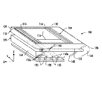
bumps, facets or
steps rising above the fourth surface. The light coupling portion may have
substantially the
same area as the light emitting portion. The light coupling portion may have
substantially the
same footprint as the light emitting portion. The light coupling portion may
be substantially
coextensive with the light emitting portion. The first surface, the second
surface, the third
surface and the fourth surface may be substantially parallel to one another.
The fourth surface
may be a light emitting surface and the first surface may be disposed
substantially parallel to
1
the fourth surface where the plurality of LEDs may be spaced over the first
surface. The light
transmission portion may be substantially annular. Light may be directed
radially inwardly
from the light transmission portion into the light emitting portion. A second
light transmission
portion may optically couple the light coupling portion to the light emitting
portion.
[0004] In some embodiments, a waveguide comprises a light coupling portion
having
a first interior surface and a first exterior surface where the first exterior
surface comprises a
plurality of light coupling features. A plurality of LEDs emits light into the
light coupling
features. A light emitting portion has a second interior surface and a second
exterior surface
where the second exterior surface defines a light emitting surface. The light
emitting portion
is disposed adjacent the light coupling portion such that the first interior
surface is disposed
adjacent the second interior surface. A light transmission portion optically
couples the light
coupling portion to the light emitting portion.
[0005] The light coupling portion and light emitting portion may be separate
components connected at an interface. A light extraction feature may extract
light through the
second exterior surface. The light extraction feature may comprise at least
one of indents,
depressions, facets or holes extending into the fourth surface and bumps,
facets or steps rising
above the fourth surface. A footprint of the light coupling portion may be
substantially the
same or less than a footprint of the light emitting portion. The light
coupling portion may be
made of a first material and the light emitting region may be made of a second
material where
the first material is different than the second material. The light emitting
portion may be
made of glass and the light coupling portion may be made of at least one of
acrylic and
silicone. A second light transmission portion may optically couple the light
coupling portion
to the light emitting portion.
[0005a] In some aspects, there is provided a waveguide comprising: a light
coupling
portion having a first surface and a second surface, wherein the first surface
defines a light
coupling surface and is disposed parallel to the second surface; a first
plurality of light
coupling features arranged in rows and columns, each defming a cavity in the
first surface to
direct light into the light coupling portion; a second plurality of light
coupling features, each
defining a cavity in the second surface to direct light into the light
coupling portion; a light
emitting portion having a third surface and a fourth surface, the light
emitting portion being
disposed adjacent the light coupling portion such that the third surface is
disposed adjacent
the second surface; and a light transmission portion optically coupling the
light coupling
portion to the light emitting portion.
2
Date Recue/Date Received 2023-03-23
[0005b] In some aspects, there is provided a modular waveguide system
comprising: a
light coupling portion having a first interior surface and a first exterior
surface, the first
exterior surface comprising a first plurality of light coupling features and
the first interior
surface comprising a second plurality of light coupling features, wherein each
light coupling
feature defines a cavity and an interior face to direct light into the light
coupling portion; a
first LED board comprising a first plurality of LEDs arranged in rows and
columns, each
LED emitting light into one of the first plurality of light coupling features;
a second LED
board comprising a second plurality of LEDs arranged in rows and columns, each
LED
emitting light into one of the second plurality of light coupling features; a
first type of light
emitting portion and a second type of light emitting portion each having a
second interior
surface and a second exterior surface, the second exterior surface defining a
light emitting
surface, wherein the first type of light emitting portion and the second type
of light emitting
portion each have a different configuration and are physically separate from
the light
coupling portion; a light transmission portion optically coupling the light
coupling portion to
either one of the first type of the light emitting portion and the second type
of light emitting
portion; and an interface formed between and connecting the light coupling
portion and a
selected one of the first type of light emitting portion and the second type
of light emitting
portion, the interface physically and optically coupling the light coupling
portion and the
selected one of the first type of light emitting portion and the second type
of light emitting
portion.
BRIEF DESCRIPTION OF THE DRAWINGS
[0006] Fig. 1 is a bottom perspective view of an embodiment of a lighting
device.
[0007] Figs. 2 and 3 are exploded views of the lighting device of Fig. 1.
[0008] Fig. 4 is a side section view of an embodiment of a waveguide.
[0009] Fig. 5 is a top view of the waveguide of Fig. 4.
[0010] Fig. 6 is a bottom view of the waveguide of Fig. 4.
[0011] Fig. 7 is a first perspective view of the waveguide of Fig. 4.
[0012] Fig. 8 is a second perspective view of the waveguide of Fig. 4.
[0013] Fig. 9 is a perspective view of another embodiment of the waveguide.
[0014] Fig. 10 is a perspective view of another embodiment of the waveguide.
2a
Date Recue/Date Received 2023-03-23
CA 03130467 2021-08-16
WO 2020/205191
PCT/US2020/022229
[0015] Fig. 11 is atop view of the waveguide of Fig. 10.
[0016] Fig. 12 is aside section view of the waveguide of Fig. 10.
[0017] Fig. 13 is a side section view of another embodiment of a waveguide.
[0018] Fig. 14 is a top view of another embodiment of a waveguide.
[0019] Fig. 15 is a section view taken along line 15-15 of Fig. 14.
[0020] Fig. 16 is a top view of another embodiment of a waveguide.
[0021] Fig. 17 is a section view taken along line 17-17 of Fig. 16.
[0022] Fig. 18 is a top view of another embodiment of a waveguide.
[0023] Fig. 19 shows side section views of waveguide components of a modular
waveguide system.
[0024] Fig. 20 is a side section view of another embodiment of a waveguide.
[0025] Fig. 21 is a perspective view of another embodiment of the waveguide of
Fig.
[0026] Fig. 22 is a side section view of another embodiment of a waveguide.
DETAILED DESCRIPTION
[0027] It will be understood that, although the terms first, second, etc. may
be used
herein to describe various elements, these elements should not be limited by
these terms.
These terms are only used to distinguish one element from another. For
example, a first
element could be termed a second element, and, similarly, a second element
could be termed
a first element, without departing from the scope of the present invention. As
used herein,
the term "and/or" includes any and all combinations of one or more of the
associated listed
items.
[0028] The terminology used herein is for the purpose of describing particular
embodiments only and is not intended to be limiting of the invention. As used
herein, the
singular forms "a," "an" and "the" are intended to include the plural forms as
well, unless the
context clearly indicates otherwise. It will be further understood that the
terms "comprises"
"comprising," "includes" and/or "including" when used herein, specify the
presence of stated
features, steps, operations, elements, and/or components, but do not preclude
the presence or
addition of one or more other features, steps, operations, elements,
components, and/or
groups thereof.
[0029] Unless otherwise defined, all terms (including technical and scientific
terms)
used herein have the same meaning as commonly understood by one of ordinary
skill in the
art to which this invention belongs. It will be further understood that terms
used herein
should be interpreted as having a meaning that is consistent with their
meaning in the context
3
CA 03130467 2021-08-16
WO 2020/205191 PCT/US2020/022229
of this specification and the relevant art and will not be interpreted in an
idealized or overly
formal sense unless expressly so defined herein.
[0030] It will be understood that when an element such as a layer, region or
substrate
is referred to as being "on" or extending "onto" another element, it can be
directly on or
extend directly onto the other element or intervening elements may also be
present. In
contrast, when an element is referred to as being "directly on" or extending
"directly onto"
another element, there are no intervening elements present. It will also be
understood that
when an element is referred to as being "connected" or "coupled" to another
element, it can
be directly connected or coupled to the other element or intervening elements
may be present.
In contrast, when an element is referred to as being "directly connected" or
"directly coupled"
to another element, there are no intervening elements present.
[0031] Relative terms such as "below" or "above" or "upper" or "lower" or
"horizontal" or "lateral" or "vertical" may be used herein to describe a
relationship of one
element, layer or region to another element, layer or region as illustrated in
the figures. It
will be understood that these terms are intended to encompass different
orientations of the
device in addition to the orientation depicted in the figures.
[0032] Embodiments of the invention are described herein with reference to
cross-
section illustrations that are schematic illustrations of idealized
embodiments (and
intermediate structures) of the invention. The thickness of layers and regions
in the drawings
may be exaggerated for clarity. Additionally, variations from the shapes of
the illustrations
as a result, for example, of manufacturing techniques and/or tolerances, are
to be expected.
Thus, embodiments of the invention should not be construed as limited to the
particular
shapes of regions illustrated herein but are to include deviations in shapes
that result, for
example, from manufacturing.
[0033] In the drawings and specification, there have been disclosed typical
embodiments of the invention and, although specific terms are employed, they
are used in a
generic and descriptive sense only and not for purposes of limitation, the
scope of the
invention being set forth in the following claims.
[0034] Figs. 1 through 3 show an embodiment of the waveguide of the invention
in an
example embodiment of a lighting device 36. While one embodiment of a lighting
device is
shown and described with reference to Figs. 1 to 3, lighting devices using the
waveguides as
disclosed herein may take many other forms and may be used in lighting
applications other
than as specifically shown and described herein. The lighting device shown and
described
herein is for explanatory purposes and is not intended to limit the
applicability of the
4
CA 03130467 2021-08-16
WO 2020/205191 PCT/US2020/022229
waveguides as disclosed herein. Lighting device 36 is suitable for outdoor
applications such
as in a parking lot or roadway and is capable of being mounted on a stanchion,
pole or other
support structure. Lighting devices that take advantage of the waveguides
disclosed herein
may take many other forms.
[0035] As shown in Figs. 1 through 3, the lighting device 36 comprises a
housing 40
and a head assembly 42. The housing 40 comprises a top housing portion 44 and
a bottom
housing portion 45. The top housing portion 44 comprises a top surface 48, a
front wall 52,
and side walls 56. A communication component 60 such as an RF antenna that
senses RF
energy, a light sensor or the like may be disposed in a receptacle 64 in the
housing 40. The
communication component may be located at any suitable position on the
lighting device and
more than one communication component may be used. An upper convection opening
72 is
disposed in the top housing portion 44. The bottom housing portion 45
comprises a lower
convection opening 78 disposed below the upper convection opening 72.
[0036] The head assembly 42 is at least partially enclosed by the housing 40
and
comprises an optical assembly 80. The optical assembly 80 comprises a
waveguide 100, a
light source 123, a lower frame member 86 partially surrounding the waveguide
100 and
forming a barrier between the waveguide 100 and the housing 40, and an upper
frame
member 87 disposed above the optical waveguide 100. The light source 123
comprises a
plurality of LEDs 125 (Fig. 4) supported on an LED board 128 and disposed
adjacent the
waveguide 100 to direct light into the waveguide 100. The head assembly 42
further
comprises a driver housing 94 that contains the LED driver circuit and other
lamp electronics
122 (Fig. 4) to drive LEDs 125. A reflective bottom surface of the upper frame
member 87
may be disposed adjacent one or more exterior surfaces of the optical
waveguide 100.
[0037] The LED driver circuit and other lamp electronics 122 may be disposed
in the
driver housing 94, which is disposed proximal to the LEDs 125 on LED board
128. The
driver housing 94 may comprise an upper portion 94-1 and a lower portion 94-2.
The upper
portion 94-1 forms a top cover of the driver housing 94. Part of the driver
housing 94 may be
made of a metal capable of efficient heat transfer.
[0038] A heat exchanger 96 is included in the housing 40. The heat exchanger
96 may
comprise a plurality of fins 103. The fins 103 transfer heat at least by
convection through the
upper and lower convection openings 72 and 78. The heat exchanger 96 is in
thermal
communication (via conduction, convection, and/or radiation) with the LEDs
125, LED board
128 and the LED driver circuit and other lamp electronics 122. One or more
thermally
conductive LED boards 128, such as printed circuit boards (PCBs), receive and
mount the
LEDs 125 and conduct heat therefrom_ The LED boards 128 are preferably made of
one or
more materials that efficiently conduct heat and are disposed in thermal
communication
with the heat exchanger 96. Alternative paths may be present for heat transfer
between the
LED driver circuit and other lamp electronics 122, the LEDs 125, the LED board
128 and
the heat exchanger 96, such as a combination of conduction, convection, and/or
radiation. In
the illustrated embodiments, the upper and lower convection openings 72 and 78
are
disposed above and below the heat exchanger 96, respectively, thus providing
for efficient
heat transfer via a direct vertical path of convection flow.
[0039] The bottom housing portion 45 may be opened by exerting a downward
force
on handle 136 to disconnect mating snap-fit connectors on the bottom housing
portion 45 and
the top housing portion 44. Also, as a result of the downward force, the
bottom housing
portion 45 rotates about pins 139 such that a front portion of the bottom
housing portion 45
pivots downward, thus allowing access to the interior of the housing 40. In
one embodiment,
the lighting device 36 may be placed onto a stanchion such that an end of the
stanchion
extends through a mounting aperture 144. Fasteners 140, 143 engage fastener
bores 142 to
secure the stanchion to the housing. Many other mechanisms for supporting a
light fixture
may also be used. Electrical connections may be made from a power source S to
the LED
driver circuit and other lamp electronics 122 to power the LEDs 125 (Fig. 4).
[0040] Each LED 125 may be a single white LED or multiple white LEDs or each
may
comprise multiple LEDs either mounted separately or together on a single
substrate or package
including a phosphor-coated LED either alone or in combination with a color
LED, such as a
green LED, etc. Details of suitable arrangements of the LEDs and lamp
electronics for use in
the light fixture are disclosed in U.S. Patent No. 9,786,639, entitled "Solid
State Light Fixtures
Suitable for High Temperature Operation Having Separate Blue-Shifted-
Yellow/Green and
Blue-Shifted-Red Emitters" issued on October 10,2017. In other embodiments,
all similarly
colored LEDs may be used where for example all warm white LEDs or all cool
white LEDs
may be used where all of the LEDs emit at a similar color point. In such an
embodiment all of
the LEDs are intended to emit at a similar targeted wavelength; however, in
practice there may
be some variation in the emitted color of each of the LEDs such that the LEDs
may be selected
such that light emitted by the LEDs is balanced such that the lighting device
36 emits light at
the desired color point. In the embodiments disclosed herein a various
combinations of LEDs
of similar and different colors may be selected to achieve a desired color
point. Each LED
element or module may be a single white or other color LED chip or other bare
6
Date Recue/Date Received 2023-03-23
component, or each may comprise multiple LEDs either mounted separately or
together on a
single substrate or package to form a module including, for example, at least
one phosphor-
coated LED either alone or in combination with at least one color LED, such as
a green LED,
a yellow LED, a red LED, etc. In those cases where a soft white illumination
is to be
produced, each LED 125 typically may include one or more blue shifted yellow
LEDs and
one or more red LEDs. The LEDs may be disposed in different configurations
and/or layouts
as desired. Different color temperatures and appearances may be produced using
other LED
combinations, as is known in the art. In one embodiment, the light source 123
comprises any
LED, for example, an MT-G LED module incorporating TrueWhite LED technology
or as
disclosed in U.S. Pat. No. 9,818,919, issued to Lowes et al. on November 14,
2017, entitled
"LED Package with Multiple Element Light Source and Encapsulant Having Planar
Surfaces"
by both as developed by Cree, Inc., the assignee of the present application.
In any of the
embodiments disclosed herein the LEDs 125 may have a lambertian light
distribution,
although each may have a directional emission distribution (e.g., a side
emitting distribution),
as necessary or desirable. More generally, any lambertian, symmetric, wide
angle,
preferential-sided, or asymmetric beam pattern LED(s) may be used as the light
source.
Various types of LEDs may be used, including LEDs having primary optics as
well as bare
LED chips. The LEDs 125 may be disposed in different configurations and/or
layouts as
desired. Different color temperatures and appearances could be produced using
other LED
combinations, as is known in the art. For example, a side emitting LED
disclosed in U.S. Pat.
No. 8,541,795 may be utilized. Still further, any of the LED arrangements and
optical
elements disclosed in co-pending U.S. Pat. No. 9,869,432, filed Dec. 9, 2013,
entitled
"Luminaires Using Waveguide Bodies and Optical Elements" by Keller et al., may
be used.
[0041] Referring to Figs. 4 ¨ 7, the LEDs 125 are shown mounted on a substrate
or
LED board 128. The LED board 128 may be any appropriate board, such as a PCB,
flexible
circuit board, metal core circuit board or the like with the LEDs 125 mounted
and electrically
interconnected thereon. The LED board 128 can include the electronics and
interconnections
necessary to deliver power to the LEDs 125. The LED board 128 may provide the
physical
support for the LEDs 125 and may form part of the electrical path to the LEDs
125 for
delivering current to the LEDs 125. If desired, a surface 130 of LED board 128
may be
covered or coated by a reflective material, which may be a white material or a
material that
exhibits specular reflective characteristics. The LED board 128 is secured in
fixed relation to
7
Date Recue/Date Received 2023-07-05
the waveguide 100 in any suitable fashion such that the LEDs 125 are disposed
opposite to
the light coupling portion 124 as will be described.
[0042] The LEDs 125 emit light when energized through the electrical path. The
term
"electrical path" is used to refer to the entire electrical path to the LEDs
125, including an
intervening driver circuit and other lamp electronics 122 in the lighting
device disposed
between the source of electrical power S and the LEDs 125. Electrical
conductors (not
shown) run between the LEDs 125, the driver circuit and other lamp electronics
122 and the
source of electrical power S, such as an electrical grid, to provide critical
current to the LEDs
125. The driver circuit and other lamp electronics 122 may be located remotely
in driver
housing 94, the driver circuit and other lamp electronics 122 may be disposed
on the LED
board 128 or a portion of the driver circuit and other lamp electronics 122
may be disposed
on the LED board 128 and the leinainder of the driver circuit and other lamp
electronics 122
may be remotely located. The driver circuit and other lamp electronics 122 are
electrically
coupled to the LED board 128 and are in the electrical path to the LEDs 125.
LED lighting
systems can work with a variety of different types of power supplies or
drivers. For example,
a buck converter, boost converter, buck-boost converter, or single ended
primary inductor
converter (SEP1C) could all be used as driver or a portion of a driver for an
LED fighting
device or solid-state lamp. The driver circuit may rectify high voltage AC
current to low
voltage DC current, and regulate current flow to the LEDs. The power source S
can be a
battery or, more typically, an AC source such as the utility mains. The driver
circuit is
designed to operate the LEDs 125 with AC or DC power in a desired fashion to
produce light
of a desired intensity and appearance. The driver circuit may comprise a
driver circuit as
disclosed in U.S. Pat. No. 9,791,110 issued on Oct. 17, 2017, entitled "High
Efficiency
Driver Circuit with Fast Response" by Hu et al. or U.S. Pat. No. 9,303,823,
issued on Apr. 5,
2016, entitled "SEPIC Driver Circuit with Low Input Current Ripple" by Hu et
al. The driver
circuit may further be used with light control circuitry that controls color
temperature of any
of the embodiments disclosed herein in accordance with user input such as
disclosed in U.S.
patent application Ser. No. 14/292,286, filed May 30, 2014, entitled "Lighting
Fixture
Providing Variable CCT" by Pope et al. Preferably, the light source 123
develops light
appropriate for general illumination purposes.
[0043] The light emitted by the LEDs 125 is delivered to waveguide 100 for
further
treatment and distribution of the light as will be described in detail. The
waveguide 100 may
8
Date Recue/Date Received 2023-03-23
be used to mix the light emitted by the LEDs 125 and to emit the light in a
directional or
omnidirectional manner to produce a desired luminance pattern.
[0044] Further, any of the embodiments disclosed herein may include one or
more
communication components 60 forming a part of the light control circuitry,
such as an RF
antenna that senses RF energy or a light sensor. The communication components
may be
included, for example, to allow the luminaire to communicate with other
luminaires and/or
with an external controller such as a wireless remote control. More generally,
the control
circuitry includes at least one of a network component, an RF component, a
control
component, and a sensor. The sensor may provide an indication of ambient
lighting levels
thereto and/or occupancy within the illuminated area. The communication
components such as
a sensor, RF components or the like may be mounted as part of the housing or
lens assembly.
Such a sensor may be integrated into the light control circuitry. The
communication
components may be connected to the lighting device via a 7-pin NEMA photocell
receptacle
or other connection. In various embodiments described herein various smart
technologies may
be incorporated in the, lamps as described in the following United States
patent applications
"Solid State Lighting Switches and Fixtures Providing Selectively Linked
Dimming and Color
Control and Methods of Operating," United States Patent No. 8,736,186, issued
May 27,
2014; "Master/Slave Arrangement for Lighting Fixture Modules," U.S. Patent No.
9,572,226,
issued February 14, 2017; "Lighting Fixture for Automated Grouping," U.S.
Patent No.
9,155,165, issued October 6, 2015; "Multi-Agent Intelligent Lighting System,"
U.S. Patent
No. 8,975,827, issued March 1, 2013; "Routing Table Improvements for Wireless
Lighting
Networks," U.S. Patent No. 9,155,166, issued October 6, 2015; "Commissioning
Device for
Multi-Node Sensor and Control Networks," U.S. Patent No. 9,433,061, issued
August 30,
2016; "Wireless Network Initialization for Lighting Systems," U.S. Patent No.
8,829,821,
issued September 9,2014; "Commissioning for a Lighting Network," U.S. Patent
No.
8,912,735, issued December 16, 2014; "Ambient Light Monitoring in a Lighting
Fixture,"
Application Number 13/838,398, filed March 15, 2013; "System, Devices and
Methods for
Controlling One or More Lights," U.S. Patent No. 9,622,321, issued Aptil 11,
2017;
9
Date Recue/Date Received 2023-03-23
and "Enhanced Network Lighting," Application Number 61/932,058, filed January
27, 2014.
Additionally, any of the light fixtures described herein can include the smart
lighting control
technologies disclosed in U.S. Application No. 2017/02310668, titled
"Automatic Mapping
of Devices in a Distributed Lighting Network", filed on June 24, 2016 to
Roberts et al. and
assigned to the same assignee as the present application.
[0045] The lighting device 36 of Figs. 1 - 3 is an embodiment of a solid state
lighting device suitable for use in outdoor applications; however, the system
of the
invention may be used in any solid state lighting device. Moreover, while an
embodiment of
a lighting device is shown and described, the waveguides as disclosed herein
may be used in
any solid state lighting device including lamps, luminaires, troffer-style
lights, outdoor
lighting or the like. The LEDs, waveguide, power circuit and other components
may be
housed in any suitable housing. The lighting devices described herein may be
used for any
suitable application in any environment such as interior lighting or exterior
lighting. The
lighting device may be used as a troffer luminaire, suspended luminaire,
recessed lighting,
street/road way lighting, parking garage lighting or the like. The housing may
be configured
for the particular application and the light emitting portion of the waveguide
may provide
any suitable illumination pattern. Moreover, the number and type of LEDs used,
and the
total lumen output, color and other characteristics of the lighting device may
be adjusted for
the particular application.
[0046] In different lighting applications, the footprint of the waveguide is
limited by
the size constraints of the housing containing the waveguide and other
lighting device
components. For example, some lighting devices are built to fit predetermined
standardized
sizes. In other applications, such as streetlights, the size of the lighting
device is limited by
factors such as IP ratings, wind loading, and fixture weight. In other
applications the size of
the lighting device is limited by custom, aesthetic considerations,
architectural considerations
or the like. In a typical LED based lighting device, the light output of the
lighting device is
dictated by the size and number of the LEDs and the power at which the LEDs
are operated;
however, the greater the number of LEDs and the higher power at which the LEDs
are
operated, the greater the heat generated by the LEDs. In traditional
waveguides, LEDs run at
high power concentrate thermal and photonic energy into a small input coupling
region of the
waveguide, e.g. the edge of an edge lit waveguide. Because heat has a
deleterious effect on
LED output and life and can adversely affect other components, such as the
waveguide, the
Date Recue/Date Received 2023-03-23
CA 03130467 2021-08-16
WO 2020/205191
PCT/US2020/022229
=
lumen power density of the LEDs at the input coupling region is limited,
thereby limiting the
output of the lighting device. While increasing the coupling area may reduce
lumen power
density, the constraints on increasing the footprint of the lighting device,
and therefore the
waveguide, limits the expansion of the footprint of the waveguide to an extent
necessary to
lower the lumen power density. As a result, existing waveguide designs are
limited in lumen
output by the lumen power densities. Existing lighting devices also may
require extensive
heat exchanger mechanisms to prevent overheating of the system components. The
waveguides disclosed herein reduce the lumen power density at the
LED/waveguide coupling
interface to substantially reduce overheating without significantly increasing
the footprint of
the waveguide.
[0047] Referring again to Figs. 4 - 8, the waveguide 100 comprises a waveguide
body
112 that includes a light emitting portion 118, a light coupling portion 124,
and a light
transmission portion 126. The light emitting portion 118 includes a plurality
of light
extraction features 116 that extract light out of the waveguide body 112. The
light coupling
portion 124 is disposed adjacent to, and receives light emitted by, the light
source 123 and
directs light into the waveguide body 112. The light transmission portion 126
optically
couples the light emitting portion 118 to the light coupling portion 124 such
that light
introduced into the light coupling portion 124 is transmitted to the light
emitting portion 118.
[0048] The waveguide 100 may be made of any suitable optical grade material
that
exhibits total internal reflection (TIR) characteristics. The material may
comprise but is not
limited to acrylic, polycarbonate, glass, molded silicone, or the like. The
waveguide 100 has
a footprint that may be'described, generally, in terms of the area of the
waveguide in the
plane of the light emitting surface. For example, in the waveguide 100 shown
in Figs. 4 ¨ 8,
the light emitting surface 130 is a generally rectangular area of the light
emitting portion 118.
The waveguide 100 has a generally rectangular footprint (Fig. 5). The
footprint of the
waveguide 100 may be slightly greater than the area of the light emitting
surface 130 where,
for example, as shown in Fig. 4, the light transmission portion 126 extends
slightly laterally
beyond the light emitting portion 118. For a rectangular waveguide the
footprint of the
waveguide 100 may be described in terms of its length and width. For example,
the area of
the footprint of waveguide 100 may be described in terms of its length L and
width W,
transverse to the length L. While the waveguide 100 shown in Figs. 4 - 8 is
rectangular, the
waveguide may have any suitable shape including round, square, multi-sided,
oval, irregular
shaped or the like. In these and in other embodiments, the footprint of the
waveguide may be
expressed in terms other than length and width.
11
CA 03130467 2021-08-16
W02920/205191 PCT/US2020/022229
[0049] The light emitting portion 118 may be described generally as having an
exterior surface 130, an interior surface 132 and a side surface 134. The
exterior surface 130
is the light emitting surface. In the illustrated embodiment, the surfaces
comprise generally
planar walls; however, where the light emitting portion 118 has other than a
rectangular
shape, the surfaces may be defined in whole or part by curved walls, planar
walls, faceted
walls or combinations of such walls.
[0050] One or more of the surfaces of the light emitting portion 118 may be
formed
with light extraction features 116 to define a light emitting area 114 on
light emitting surface
130 (note, the light extraction features 116 are not shown in Fig. 5 in order
to more clearly
show the light source 123). The light extraction features 116 may be formed on
the light
emitting exterior surface 130, as shown. Alternatively, the light extraction
features may be
formed on the interior surface 132 to reflect light to and out of the exterior
surface 130. In
some embodiments, the light extraction features 116 may be formed on both the
exterior
surface 130 and the interior surface 132. The light extraction features 116
may also be formed
within the waveguide body 112 at positions between the exterior and interior
surfaces 130,
132. It is to be understood that in use, the waveguides described herein may
assume any
spatial orientation and the light emitting surface 130 may be an upper surface
of the
waveguide, a lower surface of the waveguide and/or a side surface of the
waveguide. For
example, in Fig. 4 the light emitting surface 130 faces up while in the
embodiment of Figs. 1
¨3, the light emitting surface 130 faces down to produce downlight. The light
extraction
features 116 may be designed to emit light from the waveguide in any direction
and in any
illumination pattern.
[0051] Referring to Fig. 21, the light extraction features 116 may also be
formed on
the side surfaces 134 of the light emitting portion 118 such that light may
emitted laterally
from the waveguide in a direction substantially perpendicular to the direction
of the light
emitted from surface 134. The side surfaces 134 may form light emitting
surfaces in addition
to light emitting surface 130 or in place of light emitting surface 130.
[0052] The light extraction features 116 can comprise a single light
extraction
element or a plurality of individual light extraction elements. The size,
shape and/or density
of individual light extraction features 116 can be uniform or vary across one
or more surfaces
of the waveguide body 112 in a regular or irregular fashion to produce desired
light emission
pattern. The light extraction features 116 can comprise indents, depressions,
facets or holes
extending into the waveguide, or bumps, facets or steps rising above the
waveguide surface,
or a combination of both bumps and depressions. The light extraction features
116 may be
12
part of the waveguide body 112 or may be coupled to surfaces of the waveguide
body 112.
Individual light extraction features 116 may have a symmetrical or
asymmetrical shape or
geometry. The light extraction features 116 can be arranged in an array, and
may exhibit
regular or irregular spacing. The light extraction features 116 may be applied
to the
waveguide as part of the molding process of the waveguide body 112, by etching
or other
process, by application of a film containing the light extraction features or
in other manners.
One example of light extraction features is described in U.S. Patent No.
9,835,317 issued to
Yuan et al. on December 5, 2017 and entitled "Luminaire Utilizing Waveguide".
Additionally, the extraction features may comprise small indents, protrusions,
and/or
reflective materials and/or surfaces as shown in U.S. Patent No. 9,690,029,
issued to Keller
et al. on June 27, 2017 and entitled "Optical Waveguides and Luminaires
Incorporating
Same". Light extraction features and light coupling features are also shown in
U.S. Patent
No. 9,625,636, issued to Durkee et al. on April 18, 2017 and entitled "Optical
Waveguide
Bodies and Luminaires Utilizing Same". Another example of light extraction
features is
described in U.S. Patent Application No. 15/587,442 filed by Tarsa et al. on
May 5, 2017
and entitled "Waveguide-Based Light Sources with Dynamic Beam Shaping".
[0053] The light coupling portion 124 may be described generally as having an
interior surface 140, an exterior surface 142 and a side surface 144. In the
illustrated
embodiment the surfaces comprise generally planar walls; however, where the
light coupling
portion 124 has other than a rectangular shape the surfaces may be defined in
whole or part by
curved walls, planar walls, faceted walls or combinations of such walls. The
light coupling
portion 124 is arranged such that it is disposed approximately parallel to the
light emitting
portion 118 in a layered or stacked configuration. In the orientation of the
waveguide shown
in Fig_ 4 the light emitting portion 118 may be described as being over the
light coupling
portion 124 while in the orientation of the waveguide shown in Figs. 1 - 3 the
light emitting
portion 118 may be described as being under the light coupling portion 124. In
any
orientation the light emitting portion 118 and the light coupling portion 124
may be described
as being in a stacked or layered configuration. The light coupling portion 124
is spaced from
the light emitting portion 118 by a narrow air gap 129. In some embodiments,
the light
coupling portion 124 is closely spaced from the light emitting portion 118 to
minimize the
height of the waveguide in the z-direction. In this manner, the light coupling
13
Date Recue/Date Received 2023-03-23
CA 03130467 2021-08-16
WO 2020/205191
PCT/US2020/022229
portion 124 is arranged back-to-back with the light emitting portion 118. The
light coupling
portion 124 is disposed adjacent the non-light emitting interior surface 132
of the light
emitting portion 118 such that the light coupling portion 124 does not
interfere with light
emitted from the light emitting portion 118.
[0054] As is evident from Figs. 4 - 8, the light coupling portion 124 has
substantially
the same area as the light emitting portion 118 and is arranged to be
substantially coextensive
with the light emitting portion 118 such that the light coupling portion 124
does not increase
the footprint of the waveguide relative to the light emitting portion 118. In
some
embodiments, the light coupling portion 124 may have a smaller footprint than
the light
emitting portion 118 provided the lumen density at the coupling face does not
create
overheating conditions for the system components. Moreover, in some
embodiments, the
light coupling portion 124 may have a larger footprint than the light emitting
portion
provided that the increase in footprint is not an issue in the lighting
device. However, in
some preferred embodiments, the footprint of the light coupling portion 124 is
equal to or
smaller that the footprint of the light emitting portion 118 such that the
overall footprint of
the waveguide is not increased. Moreover, the light emitting portion 118 and
light coupling
portion 124 may have different shapes. While the arrangement of the light
coupling portion
124 may not increase the footprint of the waveguide, the entire exterior
surface 142 of the
light coupling portion 124 may be used as the coupling surface for the LEDs
125. As shown
in Figs. 4 - 8, an array of LEDs 125 may be positioned to input light into the
light coupling
portion 124 over substantially the entire exterior surface 142 thereof. The
spacing of the
LEDs 125 may be increased over a traditional edge lit waveguide and a greater
number of
LEDs operated at higher power may be used while still maintaining or
decreasing the lumen
power density of the device. Whether the footprint of the light coupling
portion 124 is
smaller than, larger than, or substantially the same as the footprint of the
light emitting
portion 118, the arrangement of the light guide as described herein can be
used to control the
routing of the light through the waveguide to produce any mixture of light
output patterns.
The direction, intensity and lumen density of the light may be managed
simultaneously using
the waveguide arrangements as described herein.
[0055] Each of the LEDs 125 may be optically coupled to the light coupling
portion
124 by light coupling features 150a, 150b. The light coupling features 150a
are arranged in a
one-to-one relationship with the LEDs 125 while the light coupling features
150b optically
couple more than one LED 125 to the waveguide 100. In some embodiments, all of
the light
coupling features may be in a one-to-one relationship with the LEDs, and in
other
14
CA 03130467 2021-08-16
WO 2020/205191 PCT/US2020/022229
embodiments, all of the light coupling features may be coupled to plural LEDs.
The number,
spacing and pattern of the LEDs 125 and of light coupling features 150a, 150b
may be
different than as shown herein. Light may be coupled into the waveguide
through an air gap
and a coupling cavity defined by surfaces located at an edge and/or interior
portions of the
waveguide. Such surfaces comprise an interface between the relatively low
index of
refraction of air and the relatively high index of refraction of the waveguide
material. One
way of controlling the spatial and angular spread of injected light is by
fitting each source
with a dedicated lens. These lenses can be disposed with an air gap between
the lens and the
coupling optic, or may be manufactured from the same piece of material that
defines the
waveguide's distribution element(s). The light coupling features may differ
from those
disclosed herein and may be used provide directional light into the waveguide.
[0056] As shown in Figs. 4 ¨ 8, the LEDs 125 are placed adjacent the exterior
surface
142 of the light coupling portion 124 to allow access to the LEDs 125 and to
simplify
manufacturing; however, the LEDs 125 may be arranged in the air gap 129
between the light
coupling portion 124 and the light emitting portion 118. In such an
arrangement, the LEDs
are arranged opposite the interior face 140 of the light coupling portion 124
to direct light
into the light coupling portion 124. In other embodiments, the LEDs may be
arranged
adjacent both the exterior surface 142 of the light coupling portion 124 and
in the air gap 129
between the light coupling portion 124 and the light emitting portion 118. As
shown in Fig.
20, in such an arrangement, a second light source 123a is arranged in space
129 such that the
LEDs 125a of the second light source 123a are arranged opposite the internal
face 140 of the
light coupling portion 124. The light source 123a may be powered as previously
described
with respect to light source 123. Light coupling features 150a, 150 may be
provided in face
140 to couple LEDs 125a to the waveguide. Using a first light source 123 and a
second light
source 123a increases the light directed into the waveguide and increases the
over-all lumen
output at the light emitting portion 134.
[0057] Regardless of the type of light coupling features used, the entire
surface 142 of
the light coupling portion 124 is available to couple the LEDs 125 to the
waveguide. As
shown in the embodiment of Figs. 4 - 8, the light coupling surface 142 extends
substantially
parallel to the light emitting surface 130 such that the area of the light
coupling surface is
approximately the same as the area of the light emitting surface 130. It is to
be understood
that in some embodiments, the light emitting portion 118 and the light
coupling portion 124
may be tapered or curved such that the light coupling portion 124 and the
light emitting
portion 118 may not be parallel in the strictest sense and may have slightly
different areas
CA 03130467 2021-08-16
WO 2020/205191 PCT/US2020/022229
even where the footprints of the light coupling portion 124 and the light
emitting portion 118
are the same.
[0058] The waveguide 100 is arranged such that the light coupling surface 142
is a
major surface of the waveguide. As explained above, the light coupling portion
124 has
major interior and exterior surfaces connected by much smaller side or edge
surfaces. The
areas of the major interior and exterior surfaces are significantly greater
than the area of the
side edge surfaces such that using one of the major surfaces of the waveguide
as the light
coupling surface 142 greatly reduces the density of the LEDs 125.
[0059] The light transmission portion 126 optically couples the light coupling
portion
124 to the light emitting portion 118. The light transmission portion 126
transmits the light
from the light coupling portion 124 to the light emitting portion 118 and may
be used to
condition the light. For example, the light transmission portion 126 may be
used to color mix
the light and to eliminate hot spots. In the embodiment of Figs. 4 - 8, the
light transmission
portion 126 comprises a curved or angled section of the waveguide body that
bends back over
itself to transmit the light from an edge of the light coupling portion 124 to
an edge of the
light emitting portion 118.
[0060] The light may be transmitted through the light coupling portion 124,
the light
transmission portion 126 and the light emitting portion 118 using total
internal reflection
(TIR) principles. Total internal reflection occurs when a propagating wave
strikes a medium
boundary at an angle larger than a particular critical angle with respect to
the normal to the
surface. If the refractive index is lower on the other side of the boundary
and the incident
angle is greater than the critical angle, the wave cannot pass through and is
entirely reflected.
In the waveguide 100 TIR principles may be used to transmit the light through
the
waveguide. However, in some embodiments reflectors may be used. For example,
reflectors
or a reflective material may be disposed over all a part of the light
transmission portion 126
and over parts of the light coupling portion 124 and the light emitting
portion 118. The
reflective material may comprise a specular layer, a white optic layer or the
like and may
comprise a film, paint, a physical layer or the like.
[0061] In addition to increasing the area of the light coupling surface 142,
the
waveguides as described herein also increase the functional light path of the
light traveling
from the light coupling features 150 to the light extraction features 116. As
is evident from
Figs. 4 - 8, the light path includes some, or all, of the light coupling
portion 124, some, or all,
of the light emitting portion 118 as well as the length of the light
transmission portion 126.
The light path is increased while maintaining a minimum footprint of the
waveguide. While
16
CA 03130467 2021-08-16
WO 2020/205191 PCT/US2020/022229
the z-dimension of the waveguide is increased, the x, y dimensions (as
represented by width
W and length L in Fig. 5) are not increased and typically the x, y dimensions
are the critical
dimensions in lighting device design.
[0062] In some embodiments, one or more of the light coupling portion 124, the
light
transmission portion 126 and the light emitting portion 118 may be provided
with internal
light altering features 133 for diffusing and/or reflecting the light as shown
in Fig. 22. These
internal light altering features 133 may comprise gas voids (such as air
"bubbles"), discrete
elements such as diffusive and/or specular reflective particles suspended in
or dispersed
throughout the waveguide body or other reflective, diffusive or refractive
elements such as
elongated features. The light altering features 133 may be of any suitable
shape and size, and
each of the light altering features may be of the same or different shapes and
sizes as other
ones of the light altering features. The light altering features 133 may be
dispersed uniformly
or non-uniformly in the wave guide body to alter the path of travel of the
light through the
waveguide body and to alter the light pattern of the emitted light. In some
embodiments, one
section of the waveguide body, such as the light emitting portion, may have
the light altering
features while other sections of the waveguide body, such as the light
coupling portion, may
not have the light altering features. Moreover, the density of the light
altering features may
be uniform or non-uniform throughout the waveguide.
[0063] Referring to Fig. 9, another embodiment of a waveguide 200 is
illustrated.
The embodiment of Fig. 9 is similar to that described above with reference to
Figs. 4 - 8
except that the LEDs 225a, 225b and light coupling features 250a, 250b are
arranged in
multiple groups and the light from each group is transmitted through opposing
light
transmission sections 226a, 226b such that the light of the two groups enters
the light
emitting portion 218 from opposite ends and in opposite directions. The light
emitting
portion 218 may be described generally as having an exterior surface 230, an
interior surface
232 and side or edge surfaces 234. In the illustrated embodiment, the surfaces
comprise
generally planar surfaces; however, where the light emitting portion 218 has
other than a
rectangular shape these surfaces may be defined in whole or part by curved
walls, planar
walls, faceted walls or combinations of such walls.
[0064] One or more of the surfaces of the light emitting portion may be formed
with
two groups of light extraction features 216a, 216b to define light extraction
areas 214a, 214b.
In the illustrated embodiment, the light extraction features 216a, 216b are
formed on the
exterior surface 230 to direct light out of the exterior surface 230. Exterior
surface 230 is the
light emitting surface. Alternatively, the light extraction features may be
formed on the
17
CA 03130467 2021-08-16
WO 2020/205191 PCT/US2020/022229
interior surface 232 such that the light extraction features redirect the
light to the exterior
surface 230. The light extraction features may also be formed between the
interior surface
232 and the exterior surface 230. Further, the light extraction features 216a,
216b may be
directional such that the light extraction area 214a directs light in a first
direction, to the right
as viewed in Fig. 9, and the light extraction area 214b directs light in a
second direction, to
the left as viewed in Fig. 9. The light extraction features 216a, 216b may be
configured as
previously described.
[0065] The light coupling portion 224 may be described generally as having an
interior surface 240, an exterior surface 242 and edge or side surfaces 244.
In the illustrated
embodiment, the surfaces comprise generally planar surfaces; however, where
the light
coupling portion 224 has other than a rectangular shape these surfaces may be
defined in
whole or part by curved walls, planar walls, faceted walls or combinations of
such walls. The
light coupling portion 224 is arranged such that it is disposed approximately
parallel to and
spaced closely from the light emitting portion 218 by an air gap 229. In this
manner the light
coupling portion 224 is arranged back-to-back with the light emitting portion
218. The light
coupling portion 224 is disposed adjacent the non-light emitting surface 232
of the light
emitting portion 218 such that the light coupling portion 224 does not
interfere with light
emitted from the light emitting portion 218. As is evident from Fig. 9, the
light coupling
portion 224 has substantially the same area as the light emitting portion 218
and is arranged
to be substantially coextensive with the light emitting portion 218 such that
the light coupling
portion does not increase the footprint of the waveguide relative to the light
emitting portion.
While the light coupling portion does not increase the footprint of the
waveguide, the entire
lower surface 242 of the light coupling portion 214 may be used as the
coupling surface for
the LEDs 225a, 225b.
[0066] As shown in Fig. 9, a first array of LEDs 225a may be positioned to
input light
into the light coupling portion 224 over a first section of the exterior
surface 242 thereof and
a second array of LEDs 225b may be positioned to input light into the light
coupling portion
224 over a second section of the exterior surface 242 thereof. In the
illustrated embodiment,
the number and spacing of the LEDs 225a, 225b is approximately equal; however,
the two
groups of LEDs may differ in size, number of LEDs, spacing of LEDs, types of
LEDs, or the
like. The spacing of the LEDs may be increased over a traditional edge lit
waveguide and a
greater number of LEDs operated at higher power may be used while still
maintaining or
decreasing the lumen power density.
18
CA 03130467 2021-08-16
WO 2020/205191 PCT/US2020/022229
[0067] Each of the LEDs 225a, 225b may be optically coupled to the light
coupling
portion by light coupling features 250a, 250b, respectively. The light
coupling features 250a,
250b may be arranged in a one-to-one relationship with the LEDs or a single
light coupling
feature may be used to optically couple multiple LEDs to the waveguide, as
previously
described. Regardless of the type of light coupling feature used, the entire
surface 242 of the
light coupling portion 218 is available to couple the LEDs 225a, 225b to the
waveguide. The
light coupling features may be configured such that the light emitted from the
first group of
LEDs 225a is directed in a different direction than the light emitted from the
second group of
LEDs 225b. As shown in Fig.9, the light from LEDs 225a is directed to the left
and the light
from LEDs 225b is directed to the right.
[0068] Optically coupling the light coupling portion 214 to the light emitting
portion
218 are two light transmission portions 226a, 226b, one arranged at each end
of the light
emitting portion and the light coupling portion such that light emitted from
LEDs 225a is
transmitted through light coupling portion 226a and light emitted from LEDs
225b is
transmitted through light coupling portion 226b. The light enters the light
emitting portion
218 from opposite ends thereof and travels through the light emitting portion
in opposite
directions as represented by arrows in Fig. 9. The light extraction features
216a, 216b may
be arranged such that light traveling through light emitting portion 218 in
the first direction is
emitted generally in the first direction and light traveling through light
emitting portion 218
in the second direction is emitted generally in the second direction. Because
the light is
emitted in the same general direction as it is traveling through the light
emitting portion 218
optical efficiency of the waveguide is increased as compared to a system where
a portion of
the light must be reversed against its direction of travel. The arrangement
described with
respect to Fig. 9 may be used to generate a bi-directional light pattern with
greater efficiency
than if one of the directional light patterns had to be turned against its
input direction. It is
noted that the light extraction features may be selected to generate any light
pattern including
for example, a narrow beam angle spot light, wide beam angle flood light or
the like. The
illumination pattern may be directionally asymmetrical or it may be
directionally
symmetrical.
[0069] Another embodiment of the waveguide of the invention is shown in Figs.
10 -
12. In this embodiment, the waveguide 300 has a generally circular footprint
where the light
coupling portion 324 and the light emitting portion 318 are generally
cylindrical in shape.
Light is emitted into the generally circular light coupling surface 342 of
light coupling
portion 324 by LEDs 325 mounted on LED board 328. The light may be directed
into light
19
CA 03130467 2021-08-16
WO 2020/205191 PCT/US2020/022229
coupling features 350. The light is directed radially outwardly in the light
coupling portion
324. The light is transmitted to a generally annular light transmission
portion 326. The light
transmission portion 326 transmits the light into the outer periphery of the
circular light
emitting portion 318 and the light is directed radially inwardly by the light
transmission
portion 326. The light emitting portion 318 has a light emitting surface 314
that includes
light emitting features 316. The light may be emitted from the light emitting
portion 318 in
any suitable pattern. In this and in any of the other embodiments described
herein a reflector
330 may be positioned between the light emitting portion 318 and the light
coupling portion
324 to optically isolate these portions from one another. As in the other
embodiments
described above, the light emitting portion 318 is arranged in a layer above
the light coupling
portion 324 and the two layers are separated by a small air gap 329. While the
embodiment
shown in Figs. 10 - 12 is circular, the lighting device may be oval,
rectangular or irregularly
shaped where the light is projected radially inwardly into the light emitting
portion from the
periphery of the light emitting portion 318 by the light transmission portion
324.
[0070] Another embodiment of the waveguide of the invention is shown in Fig.
13.
In this embodiment, the waveguide 400 has a generally rectangular footprint
where the light
coupling portion 424 and the light emitting portion 418 are generally
rectangular in shape.
The light coupling portion 424, light emitting portion 418 and the light
transmission portion
426 are generally arranged as explained with respect to the embodiment of
Figs. 4 through 8;
however, the light coupling portion 424 is arranged to generate collimated
light and the light
emitting portion 418 tapers from the light transmission portion 418 to its
distal end. Light is
emitted into the light coupling surface 442 of light coupling portion 424 by
LEDs 425
mounted on LED board 428. The light may be directed into light coupling
features 450. As
in the other embodiments described above, the light emitting portion 426 is
arranged in a
layer above the light coupling portion 424 and the two layers are separated by
an air gap 429.
A light transmission portion 426 optically connects the light emitting portion
418 and the
' light coupling portion 424 as previously described. In this embodiment, the
light emitting
portion 418 comprises a light emitting surface 430 formed by light emitting
features 416
comprising a plurality of stepped faces 416a connected by intermediate
surfaces 416b that
may be planar, curved, concave, scalloped or the like.
[0071] Another embodiment of the waveguide of the invention is shown in Figs.
14
and 15. In this embodiment, the waveguide 500 may have a generally circular
footprint, as
shown, or it may have a rectangular footprint. Light is emitted into the light
coupling surface
542 of light coupling portion 524 such that the light is directed radially
outwardly from the
CA 03130467 2021-08-16
WO 2020/205191 PCT/US2020/022229
light coupling portion 524. Light is emitted into the generally circular light
coupling surface
542 of light coupling portion 524 by LEDs 525 mounted on LED board 528. The
light may
be directed into light coupling features 550. The light is transmitted to a
generally annular
light transmission portion 526. The light transmission portion 526 transmits
the light into the
edge of a dome shaped light emitting portion 518. The light emitting portion
518 has a light
emitting surface 514 formed by light emitting features 516 as described above.
The light may
be emitted from the light emitting portion 518 in any suitable pattern;
however, with the
dome style light emitting portion the light may be emitted nearly
omnidirectionally. As in the
other embodiments described above, the light emitting portion 518 is arranged
in a layer
above the light coupling portion 524 and the two layers are separated by an
air gap 529. Figs.
16 and 17, show another embodiment of a waveguide 600 that is similar to the
waveguide of
Figs. 14 and 15 (where like reference numbers are used to identify the same
elements) except
that the light emitting portion 618 is formed as a shallower dome and is more
closely spaced
to the light coupling portion 524.
[0072] Another embodiment of the waveguide of the invention is shown in Fig.
18.
The waveguide that is similar to the waveguide of Figs. 14 - 17 (where like
reference
numbers are used to identify the same elements) except that the light coupling
portion, light
emitting portion 618 and the light transmission portion extend linearly to
create an elongated,
linear waveguide. It should be noted that in this and in the other embodiments
described
herein the relative dimensions of the waveguide in the x, y, z directions may
be different than
as shown, such that the waveguides may be relatively longer, wider or narrower
than as
specifically shown herein. For example, the width dimension W, as shown in
Fig. 5, may be
increased relative to the length L to create a linear waveguide.
[0073] In the embodiments described above, the light coupling portion, light
emitting
portion and the light transmission portion are formed as part of an integral,
one-piece
waveguide. In the embodiments described above, the waveguide may be made of a
single
piece of material or the waveguide may be made of separate pieces connected
together to
create the unitary structure. For example the light emitting portion, the
light coupling portion
and the light transmission portion may be molded as a single piece. In other
embodiments,
the light coupling portion and the light transmission portion may be molded as
a single piece
and the light emitting portion may be molded as a separate piece. The pieces
may be
designed specifically to be optically coupled to one another to create a
finished waveguide.
[0074] However, in other embodiments, a standardized light coupling portion
may be
designed to be used with multiple different types of light emitting sections
as shown in Fig.
21
CA 03130467 2021-08-16
WO 2020/205191 PCT/US2020/022229
19. In such embodiments, the light coupling portion 124a may be formed
separately from a
plurality of the light emitting portions 118a, 118b, 118c such that the light
coupling portion
124a may be optically connected to any one of a plurality of light emitting
portions. In the
illustrated embodiment each of the light coupling portion 124a and the light
emitting portions
118a, 118b, 118c include a portion of the light transmission portion 126.
However, the light
transmission portion 126 may be entirely contained within one of the light
coupling portion
or the light emitting portions. Moreover, each of the light transmission
portion, the light
coupling portion and the light emitting portion may be formed separately. An
interface 800 is
created on the light coupling portion 124a that optically couples the light
coupling portion
124a to a mating interface 802 provided on any one of the plurality of
different types of light
emitting portions 118a, 118b, and 118c. The interfaces 801, 802 may comprise
mechanical
connectors to secure the portions to one another and an optical gel or other
medium may be
used between the portions to optically couple the portions to one another. In
this manner a
single light coupling portion may be used with different types of light
emitting portions
and/or light transmission portions. For example, as shown in Fig. 19 the light
emitting
portion 118a may be substantially similar to the light emitting portion
described with respect
to Figs. 4 ¨ 8; the light emitting portion 118c may be substantially similar
to the light
emitting portion described with respect to Fig. 13; and the light emitting
portion 118b may be
similar to the light emitting portion of Figs. 4 ¨ 8 except that the light
emitting portion 118b
may be circular rather than rectangular. While examples of different types of
light emitting
portions are shown, it is to be understood that the light emitting portions
may differ from one
another in ways different than as specifically described. Moreover, different
types of light
coupling portions 124a, 124b may also be provided. For example light coupling
portion 124a
may be substantially similar to the light coupling portion described with
respect to Figs. 4
8; and the light emitting portion 124b may be substantially similar to the
light emitting
portion described with respect to Fig. 13. While examples of different types
of light coupling
portions are shown it is to be understood that the light coupling portions may
differ from one
another in ways different than as specifically described. For example,
referring to Figs. 15
and 17, the domed light emitting portions 518, 618 may be coupled to the same
type of light
coupling portion 542 at interfaces 902. The modular approach as described
herein allows the
number of components to be reduced where, for example, a single light coupling
portion may
be used with a variety of different types of light emitting portions to create
different types of
waveguides.
22
CA 03130467 2021-08-16
WO 2020/205191 PCT/US2020/022229
[0075] In some embodiments, different portions of the waveguide may be made of
different materials to provide different portions of the waveguide with
different optical
properties. For example, the light emitting portions may be formed of glass
while the light
coupling portion may be formed of a different material such acrylic or
silicone. In other
embodiments the light extracting region may be formed of silicone while the
remainder of the
light emitting portion may be glass. Making different portions of the
waveguide of different
materials may be most easily performed where the light guide comprises
separately made
portions; however, even where the waveguide is an integral, one-piece
waveguide, different
materials may be used to create different portions of the waveguide. The
different materials
may comprise acrylic, polycarbonate, glass, molded silicone, other optical
materials or
combinations of such materials. Moreover, the materials may include particles,
additives, or
the like that alter the optical properties such that, for example, one portion
of the waveguide
may be made of acrylic and a second portion of the waveguide may be made of
acrylic
containing reflective or diffusive particles. In such an embodiment, the
acrylic and acrylic
containing particles are considered different materials. Other materials and
in combinations
other than as described herein may be used to create different portions of the
waveguide
having different optical properties.
[0076] The waveguide(s) 100 described herein may comprise additional features
to
assist in developing the target illumination distribution(s). The embodiments
discussed herein
may incorporate reflecting and/or diffusing surface coverings/coatings. The
coverings/coatings may take the form of reflecting/diffusing coatings, paints,
and/or sprays as
applied to metals, plastics, papers, and/or films. Further, the
coverings/coatings contemplated
herein may take the form of reflecting/diffusing films and/or sheets including
paper films,
plastic films, paper sheets, plastics sheets, and/or metal sheets. The
reflecting/diffusing films,
coatings, paints, sheets, and/or sprays may have the same and/or different
reflecting and/or
diffusing properties. Further, the films, coatings, paints, sheets, and/or
sprays may be applied
to provide more or less coverage of the example waveguide(s). Still further,
the films,
coatings, paints, and/or sprays may be applied to particular parts while not
being applied to
other parts. The films, coatings, paints, sheets, and/or sprays may be applied
during or after
manufacture of the waveguide(s) 100, and before, during, and/or after the
manufacture and/or
assembly of the lighting systems. The films, coatings, paints, sheets, and/or
sprays
contemplated by this disclosure are referred to as coatings and films,
although use of these
terms referentially should not limit the materials/substances added to the
waveguide.
23
CA 03130467 2021-08-16
WO 2020/205191
PCT/US2020/022229
[0077] Although specific embodiments have been shown and described herein,
those
of ordinary skill in the art appreciate that any arrangement, which is
calculated to achieve the
same purpose, may be substituted for the specific embodiments shown and that
the invention
has other applications in other environments. This application is intended to
cover any
adaptations or variations of the present invention. The following claims are
in no way
intended to limit the scope of the invention to the specific embodiments
described herein.
24