Note: Descriptions are shown in the official language in which they were submitted.
ELECTRON BEAM LITHOGRAPHY WITH A BILAYER RESIST
BACKGROUND INFORMATION
Field:
The present disclosure relates generally to semiconductors and, in particular,
to a
method for forming semiconductor structures for quantum applications using
electron
beam lithography with a bilayer resist system.
Background:
Multistep processes are employed to fabricate semiconductor and quantum
devices. These processes include a sequence of lithography and chemical
processing
steps during which circuits and quantum devices can be created on a wafer.
Integrated
circuits can be fabricated such that millions of electrical or quantum
components can be
present in an area of about one centimeter. With respect to quantum devices, a
tight
control over pattern geometries and contaminants is desirable.
With shrinking features, issues such as mask alignment, resolution,
contamination,
and defects become a greater concern in fabricating devices. For example, with
feature
widths that are 10 micrometers or less, particles present in the air during
the application
can add to potential contamination and increase defects.
With respect to feature sizes, electron beam lithography can be used. Electron
beam lithography is a process in which a focused beam of electrons is scanned
to draw
shapes on a structure covered with a resist. The electron beam changes the
solubility of
a resist enabling selective removal of either the exposed or nonexposed
regions of the
resist by immersing a structure with a film in a solvent. With electron beam
lithography,
very small patterns such as sub-10 nanometers can be achieved.
Although electron beam lithography is a useful technology that can enable the
patterning of features below 10 nanometer dimensions, other issues are still
present with
a reduction in size of the features. Contamination and electron scattering
within the resist
and from the substrate are examples of other concerns that increase as the
size of the
features decreases. With scattering, a proximity effect occurs in which a
scattering of
1
Date Recue/Date Received 2021-09-14
electrons within the resist and the scattering of electrons from the substrate
are such that
undesired exposures of the resist occurs in regions adjacent to the intended
exposure by
the electron beam. As the size of the features decrease, issues with undesired
exposures
caused by a proximity effect increase.
Therefore, it would be desirable to have a method and apparatus that take into
account at least some of the issues discussed above, as well as other possible
issues.
For example, it would be desirable to have a method and apparatus that
overcome a
technical problem with electron beam lithography used in manufacturing
devices.
SUMMARY
An embodiment of the present disclosure provides a method for processing a
material stack. A hydrogen silsesquioxane layer is deposited on the material
stack. An
aluminum layer is deposited on the hydrogen silsesquioxane layer to form a
bilayer. An
electron beam is directed through a surface of the bilayer to form an exposed
portion of
the bilayer. The bilayer is developed with tetramethylammonium hydroxide,
wherein the
tetramethylammonium hydroxide removes the aluminum layer and an unexposed
portion
of the hydrogen silsesquioxane layer, leaving the exposed portion of the
hydrogen
silsesquioxane layer on the material stack.
Another embodiment of the present disclosure provides a method for processing
a material stack. A hydrogen silsesquioxane layer is deposited on the material
stack. A
diffusion barrier layer is deposited on the hydrogen silsesquioxane layer to
form a bilayer.
The diffusion barrier layer is comprised of a material having a thickness that
increases an
amount of time before the hydrogen silsesquioxane layer ages to change a dose
in an
electron beam needed to expose the hydrogen silsesquioxane layer to obtain a
desired
width for a selected feature geometry. The electron beam is directed through a
surface
of the bilayer to form an exposed portion of the bilayer. The electron beam
applies the
dose in the exposed portion of the bilayer that is selected based on a pattern
density of
features for the material stack to have a desired level of exposure of the
hydrogen
silsesquioxane layer for the selected feature geometry. The hydrogen
silsesquioxane
2
Date Recue/Date Received 2021-09-14
layer is developed. The exposed portion of the hydrogen silsesquioxane layer
exposed
to the electron beam remains on the material stack.
Yet another embodiment of the present disclosure provides a product
management system comprising fabrication equipment and a control system. The
control
system is configured to control the fabrication equipment to deposit a
hydrogen
silsesquioxane layer on a material stack; deposit a diffusion barrier layer on
the hydrogen
silsesquioxane layer to form a bilayer, wherein the diffusion barrier layer is
comprised of
a material having a thickness that increases an amount of time before the
hydrogen
silsesquioxane layer ages to change a dose in an electron beam needed to
expose the
hydrogen silsesquioxane layer for a desired width a selected feature geometry;
direct an
electron beam through a surface of the bilayer to form an exposed portion of
the bilayer,
wherein the electron beam applies the dose in the exposed portion of the
bilayer that is
selected based on a pattern density of features for the material stack to have
a desired
level of exposure of the hydrogen silsesquioxane layer for the selected
feature geometry;
and develop the hydrogen silsesquioxane layer wherein the exposed portion of
the
hydrogen silsesquioxane layer exposed to the electron beam remains on the
material
stack.The features and functions can be achieved independently in various
embodiments
of the present disclosure or may be combined in yet other embodiments in which
further
details can be seen with reference to the following description and drawings.
BRIEF DESCRIPTION OF THE DRAWINGS
The novel features believed characteristic of the illustrative embodiments are
set
forth below. The illustrative embodiments, however, as well as a preferred
mode of use,
further objectives and features thereof, will best be understood by reference
to the
following detailed description of an illustrative embodiment of the present
disclosure when
read in conjunction with the accompanying drawings, wherein:
Figure 1 is illustration of a cross-sectional view of a material
stack in accordance
with an illustrative embodiment;
3
Date Recue/Date Received 2021-09-14
Figure 2 is an illustration of a cross-sectional view of a material
stack with a
hydrogen silsesquioxane layer in accordance with an illustrative
embodiment;
Figure 3 is an illustration of a cross-sectional view of a bilayer
on a material stack
in accordance with an illustrative embodiment;
Figure 4 is an illustration of a cross-sectional view of exposing a
resist in a bilayer
in accordance with an illustrative embodiment;
Figure 5 is an illustration of a cross-sectional view of a material
stack with an
exposed portion of a hydrogen silsesquioxane layer in accordance with
an illustrative embodiment;
Figure 6 is an illustration of a cross-sectional view of an etched
material stack in
accordance with an illustrative embodiment;
Figure 7 is an illustration of a cross-sectional view of a material
stack after
etching and removal of a hydrogen silsesquioxane layer in accordance
with an illustrative embodiment;
Figure 8 is an illustration of a graph of width for a patterned
structure as a
function of predicted widths by a linear model in accordance with an
illustrative embodiment;
Figure 9 is an illustration of a graph of differences between a
width of a pattern
structure and predicted widths in accordance with an illustrative
embodiment;
Figure 10 is an illustration of a graph of exposures of devices as a
function dose
and pattern density without proximity effect corrections in accordance
with an illustrative embodiment;
Figure 11 is an illustration of a graph of exposures of devices as a
function dose
and pattern density with proximity effect corrections in accordance with
an illustrative embodiment;
Figure 12 is an illustration of a flowchart of a process for
processing a material
stack in accordance with an illustrative embodiment;
4
Date Recue/Date Received 2021-09-14
Figure 13 is an illustration of a flowchart of a process for
processing a material
stack in accordance with an illustrative embodiment;
Figure 14 is an illustration of a flowchart of a process for
processing a material
stack in accordance with an illustrative embodiment;
Figure 15 is an illustration of a flowchart of a process for processing a
material
stack in accordance with an illustrative embodiment;
Figure 16 is an illustration of a flowchart of a process for
processing a material
stack in accordance with an illustrative embodiment;
Figure 17 is an illustration of a flowchart of a process for
directing an electron
beam through a surface of a bilayer in accordance with an illustrative
embodiment; and
Figure 18 is an illustration of a block diagram of a product
management system in
accordance with an illustrative embodiment.
DETAILED DESCRIPTION
The illustrative embodiments recognize and take into account one or more
different
considerations. For example, the illustrative embodiments recognize and take
into
account that electron beam lithography can be performed using hydrogen
silsesquioxane
(HSQ) and sodium containing developers to pattern sub-10 nm resolution
features. The
illustrative embodiments recognize and take into account that sodium-based
developers
are a mobile contaminant that is incompatible with many electronic devices and
quantum
devices.
The illustrative embodiments recognize and take into account that hydrogen
silsesquioxane has a chemical instability that causes exposure characteristics
to change
.. over time. The illustrative embodiments recognize and take into account
that hydrogen
silsesquioxane is an intrinsically unstable compound. The illustrative
embodiments
recognize and take into account that the instability stems from highly mobile
and reactive
hydrogen species, which reside on the vertices of the cuboid silsesquioxane
structure.
The illustrative embodiments recognize and take into account that exposure to
energy in
the form of heat, electrons, or ultra-violet photons triggers the release of
hydrogen as
5
Date Recue/Date Received 2021-09-14
radicals. The illustrative embodiments recognize and take into account that
the radicals
diffuse catalyzing redistribution reactions which crosslink neighboring
molecules into
base-insoluble hydrogen-enriched SiOx oligomers.
The illustrative embodiments
recognize and take into account that ambient conditions are insufficiently
inert to
completely impede the reactions, resulting in a limited shelf life and
transient exposure
behaviors-
The illustrative embodiments recognize and take into account that the dose of
an
electron beam needed to expose a film of hydrogen silsesquioxane can change
over time
as hydrogen silsesquioxane ages after being applied to a wafer, a substrate, a
film, or
some other material. The illustrative embodiments recognize and take into
account that
this instability can reduce the control of dimensions for devices being
manufactured.
Further, the illustrative embodiments recognize and take into account that
narrow process
margins can occur in which time for exposure and development of a hydrogen
silsesquioxane film to obtain desired results may be much narrower than
desired. The
illustrative embodiments also recognize and take into account that a proximity
effect can
have varied issues as the pattern density changes. The illustrative
embodiments
recognize and take into account that the pattern density is a density of
features.
In other words, the illustrative embodiments recognize and take into account
that
the dose applied using an electron beam may be sufficient one time to change
the
solubility of hydrogen silsesquioxane but may be insufficient at a later time.
Thus, the illustrative examples provide a method, apparatus, and system for
manufacturing a structure using electron beam lithography with a bilayer
resist system.
In one illustrative example, a hydrogen silsesquioxane layer is deposited on a
material
stack. A diffusion barrier layer is deposited on the hydrogen silsesquioxane
layer to form
a bilayer. The diffusion barrier layer is comprised of a material having a
thickness that
increases an amount of time before the hydrogen silsesquioxane layer ages to
change a
dose in an electron beam needed to expose the hydrogen silsesquioxane layer
for a
selected feature geometry with a desired width. The electron beam is directed
through a
surface of the bilayer to form an exposed portion of the bilayer. The electron
beam applies
the dose in the exposed portion of the bilayer that is selected based on a
pattern density
6
Date Recue/Date Received 2021-09-14
of features for the material stack to have a desired level of exposure of the
hydrogen
silsesquioxane layer for the selected feature geometry. The hydrogen
silsesquioxane
layer is developed. The exposed portion of the hydrogen silsesquioxane layer
exposed
to the electron beam remains on the material stack.
Example embodiments of structures and methods are disclosed herein; however,
it is to be understood that the disclosed embodiments are merely illustrative
of the
structures and methods that may be embodied in various forms. In addition,
each of the
examples given in connection with the various embodiments is intended to be
illustrative,
and not restrictive.
Further, the figures are not necessarily to scale, as some features may be
exaggerated to show details of particular components. Therefore, specific
structural and
functional details disclosed herein are not to be interpreted as limiting, but
merely as a
representative basis for teaching one skilled in the art to variously employ
the methods
and structures of the present disclosure.
For purposes of the description hereinafter, the terms "upper," "lower,"
"right," "left,"
"vertical," "horizontal," "top," "bottom," and derivatives thereof shall
relate to the illustrative
examples in the disclosure, as it is oriented in the drawing figures. The
terms "positioned
on" means that a first element, such as a first structure, is present on a
second element,
such as a second structure, wherein intervening elements, such as an interface
structure,
e.g. interface layer, may be present between the first element and the second
element.
In this disclosure, when an element, such as a layer, a region, or a
substrate, is
referred to as being "on" or "over" another element, the element can be
directly on the
other element or intervening elements can also be present. In contrast, when
an element
is referred to as being "directly on," "directly over," or "on and in direct
contact with"
another element, no intervening elements are present, and the element is in
contact with
the other element.
The processes, steps, and structures described below do not form a complete
process flow for manufacturing integrated circuits. The disclosure can be
practiced in
conjunction with integrated circuit fabrication techniques currently used in
the art, and
only so much of the commonly practiced process steps are included as necessary
for an
7
Date Recue/Date Received 2021-09-14
understanding of the different examples of the present disclosure. The figures
represent
cross-sections of a portion of an integrated circuit during fabrication and
are not drawn to
scale, but instead are drawn so as to illustrate different illustrative
features of the
disclosure.
With reference now to Figures 1-7, illustrations of cross-sections in a
process to
form a semiconductor structure are depicted in accordance with an illustrative
embodiment. These cross-sections are illustrated to show various steps in
processing a
material stack and are not inclusive of all the steps that may be used. Other
steps may
be omitted to avoid obscuring a description of features for electron beam
lithography
using a bilayer resist system.
In Figure 1, an illustration of a cross-sectional view of a material stack is
depicted
in accordance with an illustrative embodiment. In this illustrative example,
material stack
100 can take a number of different forms. For example, material stack 100 can
be at
least one of a wafer or a set of layers. Wafers can take various forms. For
example, a
wafer can be a silicon wafer, a silicon carbide wafer, or some other type of
wafer.
As used herein, the phrase "at least one of," when used with a list of items,
means
different combinations of one or more of the listed items can be used, and
only one of
each item in the list may be needed. In other words, "at least one of' means
any
combination of items and number of items may be used from the list, but not
all of the
items in the list are required. The item can be a particular object, a thing,
or a category.
For example, without limitation, "at least one of item A, item B, or item C"
may
include item A, item A and item B, or item B. This example also may include
item A, item
B, and item C or item B and item C. Of course, any combinations of these items
can be
present. In some illustrative examples, "at least one of' can be, for example,
without
limitation, two of item A; one of item B; and ten of item C; four of item B
and seven of item
C; or other suitable combinations.
As used herein, a "set of," when used with reference to items, means one or
more
items. For example, a "set of layers" is one or more layers.
A wafer can also be referred to as a slice or a substrate. A wafer can be a
thin
slice of semiconductor or some other material that is used to fabricate
integrated circuits,
8
Date Recue/Date Received 2021-09-14
solar cells, quantum bits, quantum memories, or other devices. A layer is a
thickness for
a film comprised of the material that is to be processed in forming a device.
For example,
the layer can be a thin film which is a layer of material ranging from
fractions of a
nanometer to several micrometers in thickness.
In this illustrative example, prior processing and etching is not shown for
material
stack 100. In other illustrative examples, the process can be applied after
other etching
or processing steps for material stack 100.
Turning next to Figure 2, an illustration of a cross-sectional view of a
material stack
with a hydrogen silsesquioxane layer is depicted in accordance with an
illustrative
embodiment. In this illustrative example, hydrogen silsesquioxane layer 200
has been
deposited on material stack 100.
The deposition of hydrogen silsesquioxane to form hydrogen silsesquioxane
layer
200 can be performed through various semiconductor techniques including spin
coating.
Spin coating can be used to apply films on substrates such as material stack
100.
Hydrogen silsesquioxane layer 200 is a thin film layer that can be useful for
fabricating
quantum devices and semiconductors including quantum bits for a quantum
memory.
In this illustrative example, the thickness of hydrogen silsesquioxane layer
200 can
vary depending on the particular implementation. In one illustrative example,
the
thickness of hydrogen silsesquioxane layer 200 can be from about 20 nm to
about 100
nm.
With reference next to Figure 3, an illustration of a cross-sectional view of
a bilayer
on a material stack is depicted in accordance with an illustrative embodiment.
As
depicted, diffusion barrier layer 300 has been deposited on hydrogen
silsesquioxane layer
200 to form bilayer 302. Bilayer 302 can also be referred to as a bilayer
resist.
In this illustrative example, diffusion barrier layer 300 can be comprised of
one or
more materials. The particular material selected can be based on reducing at
least one
of contaminants for aging of hydrogen silsesquioxane layer 200. For example,
at least
one of the material or thickness of diffusion barrier layer 300 can be
selected to reduce
or prevent contaminants from entering hydrogen silsesquioxane layer 200.
9
Date Recue/Date Received 2021-09-14
Additionally, diffusion barrier layer 300 can also be selected such that aging
of
hydrogen silsesquioxane layer 200 is reduced. In other words, the aging can be
slowed
down such that a longer period of time is available before hydrogen
silsesquioxane layer
200 ages to change a dose in an electron beam needed to expose hydrogen
silsesquioxane layer 200 to obtain a desired width for a selected feature
geometry. For
example, the period of time from which hydrogen silsesquioxane layer 200 is
formed until
the time hydrogen silsesquioxane layer 200 ages such that a width can increase
to an
undesired value can be shorter than desired without diffusion barrier layer
300. For
example, the times can be (1) performing exposure within four hours and (2)
completing
the developing process within 20 hours of forming hydrogen silsesquioxane
layer 200
without diffusion barrier layer 300.
With diffusion barrier layer 300, the time to perform electron beam scanning
for
exposure can be increased to 50 hours with a completion time for developing
hydrogen
silsesquioxane layer 200 to 250 hours. In this manner, a window of time during
which
processing should occur can be greater and become less critical with respect
to obtaining
desired results.
For example, diffusion barrier layer 300 in bilayer 302 can be selected from
at least
one of aluminum, aluminum oxide, titanium, or some other suitable material
that can be
used as a diffusion barrier
In the depicted example, the material and a thickness of the material used in
diffusion barrier layer 300 is selected to increase the amount of time before
hydrogen
silsesquioxane layer 200 ages to change a dose in an electron beam needed to
expose
hydrogen silsesquioxane layer 200.
Further, the mass thickness of diffusion barrier layer 300 in bilayer 302 is
selected
to decrease scattering of the electron beam to obtain a desired width of a
selected feature
geometry. The mass thickness of a material is the actual thickness of the
material times
the density of the material. In this illustrative example, the feature can be
selected from
at least one of a gate, a lead, a line, or any other geometric shape or
configuration. In
this illustrative example, the width can be a distance between different
points on the
Date Recue/Date Received 2021-09-14
feature. For example, the width can be from edge-to-edge, corner-to-corner, or
some
other reference points or locations for the selected geometry for the feature.
When a metal, such as aluminum, is used, evaporation of the aluminum can be
performed to deposit the aluminum on hydrogen silsesquioxane layer 200 to form
diffusion barrier layer 300 in the form of an aluminum layer.
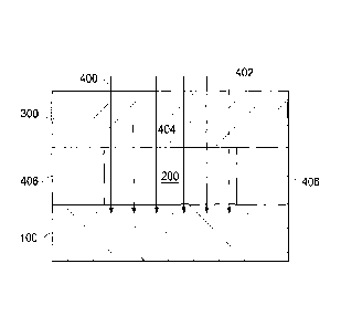
Turning now to Figure 4, an illustration of a cross-sectional view of exposing
a
resist in a bilayer is depicted in accordance with an illustrative embodiment.
In this
illustrative example, electron beam 400 can be directed through surface 402 of
bilayer
302 to expose portions of hydrogen silsesquioxane layer 200. As a result,
hydrogen
silsesquioxane layer 200 has exposed portion 404 and unexposed portion 406.
In this illustrative example, hydrogen silsesquioxane in hydrogen
silsesquioxane
layer 200 is a negative tone resist. With a negative tone resist, portions of
hydrogen
silsesquioxane in hydrogen silsesquioxane layer 200 exposed by electrons from
electron
beam 400 become unremovable when a developer is used to develop hydrogen
silsesquioxane layer 200.
With reference next to Figure 5, an illustration of a cross-sectional view of
a
material stack with an exposed portion of a hydrogen silsesquioxane layer is
depicted in
accordance with an illustrative embodiment. As can be seen in this view,
exposed portion
404 of hydrogen silsesquioxane layer 200 remains on material stack 100 after
developing
the resist, hydrogen silsesquioxane layer 200. Unexposed portion 406 in Figure
4 of
hydrogen silsesquioxane layer 200 has been removed.
In this cross-sectional view, exposed portion 404 of hydrogen silsesquioxane
layer
200 remains for use in etching material stack 100.
In this illustrative example, depending on the type of developer used,
diffusion
barrier layer 300 may be removed prior to exposing hydrogen silsesquioxane
layer 200
to a developer. The developer can be selected such that the developer removes
portions
of bilayer 302 including all of diffusion barrier layer 300 and unexposed
portion 406 of
hydrogen silsesquioxane layer 200.
For example, diffusion barrier layer 300 can be an aluminum layer, an aluminum
oxide layer, or some combination thereof. With this type of material for
diffusion barrier
11
Date Recue/Date Received 2021-09-14
layer 300, a developer such as tetramethylammonium hydroxide can be used. In
this
manner, an additional step of removing diffusion barrier layer 300 prior to
developing
hydrogen silsesquioxane layer 200 becomes unnecessary with the selection of
the
appropriate developer.
With reference to Figure 6, an illustration of a cross-sectional view of an
etched
material stack is depicted in accordance with an illustrative embodiment. As
depicted,
material stack 100 with exposed portion 404 of hydrogen silsesquioxane layer
200 has
been etched. In this example, the etching can be performed using various
techniques.
For example, the type of etching performed can be selected from at least one
of wet
etching, anisotropic etching, dry etching, plasma etching, or other suitable
etching
techniques.
As depicted, portions of material stack 100 not covered by exposed portion 404
of
hydrogen silsesquioxane layer 200 has been removed. In this illustrative
example, when
material stack 100 is a set of layers, the entire set of layers is removed. In
other illustrative
examples, the etching can be such that only a portion of the set of layers is
removed from
material stack 100 as shown by regions 602 within dashed line 600. In another
example,
when material stack 100 is a wafer substrate, a portion of material stack 100
is removed
with the remaining portion indicated by dashed line 600.
Turning now to Figure 7, an illustration of a cross-sectional view of a
material stack
after etching and removal of a hydrogen silsesquioxane layer is depicted in
accordance
with an illustrative embodiment. As depicted in this cross-sectional view,
exposed portion
404 of hydrogen silsesquioxane layer 200 has been removed. In this view, the
resulting
structure or geometry for material stack 100 is shown. Additional lithography
in etching
steps can be performed to create different features to form a set of
structures from
material stack 100.
For example, the set of structures formed from material stack 100 can be
selected
from at least one of a quantum bit, a quantum dot qubit, a waveguide, an
optical
waveguide, an optical resonator, a photon emitting quantum memory, a
transistor, or
some other suitable type of structure. In this depicted example, a quantum dot
qubit is a
quantum bit that uses semiconductor quantum dots.
12
Date Recue/Date Received 2021-09-14
The illustration of the cross-sectional views illustrating steps for
performing
electron beam lithography with a bilayer resist. Bilayer 302 in Figures 1-7 is
not meant
to imply physical or architectural limitations to the manner in which an
illustrative
embodiment may be implemented. Other components in addition to or in place of
the
ones illustrated may be used. Some components may be unnecessary. Also, the
blocks
are presented to illustrate some functional components. One or more of these
blocks
may be combined, divided, or combined and divided into different blocks when
implemented in an illustrative embodiment.
For example, diffusion barrier layer 300 can be comprised of sub layers such
as,
for example, an aluminum layer and an aluminum oxide layer. As another
example,
additional processing steps for creating features for a set of structures from
material stack
100 can be performed although not shown. The steps include other electron beam
lithography steps, other etching, doping, or implantation steps to form
desired features
for structures using material stack 100 as a starting point or intermediate
point.
Additionally, material stack 100 may have been previously etched and may
include
cavities, doped regions, or other features not depicted in material stack 100.
Turning next to Figure 8, an illustration of a graph of width fora patterned
structure
as a function of predicted widths by a linear model is depicted in accordance
with an
illustrative embodiment. In this illustrative example, graphic 800 is a graph
of width wg in
nm on y-axis 802 for patterned structured 804 as a function of predicted
widths wg* in nm
on x-axis 806 for patterned structure 804.
The predicted widths are predicted by linear model based on five independent
experimental variables in this illustrative example. In this example, the five
independent
experimental variables are exposure dose, geometry of the feature, the Al cap
thickness,
developer time (time exposed to the developer TMAH), and exposure delay (time
between coating and exposure to the electron beam). In this example, r2 is
obtained from
the linear regression. A larger value of r2 means the model is better at
describing the
data. In this example, r is a Pearson correlation coefficient. As depicted,
the data points
along line 810 indicates how the width depends on experimental parameters in
this linear
model. In this graph, a geometry can be targeted when the correlation
coefficients for the
13
Date Recue/Date Received 2021-09-14
five independent experimental variables in this example are known. In this
example, the
position of an edge moves at a rate of 0.25nm/hr/edge. As a result, patterning
a 10-nm-
wide gap with +/- 1 nm tolerance means exposures should be performed in under
four
hours and be completed within 20 hours of coating. These time constraints are
undesirable in many situations.
With reference next to Figure 9, an illustration of a graph of differences
between
a width of a pattern structure and predicted widths is depicted in accordance
with an
illustrative embodiment. In this illustrative example, graph 900 illustrates
the difference
Awg between a width of the pattern structure wg in a predicted width including
the effect
of exposure delay on y-axis 902. Section 904 shows Awg based on an exposure
delay of
30 hours and 75 hours for a 0.25 nm/hr/edge without a diffusion barrier layer.
Section
906 shows Awg based on an exposure delay of 15 hours and 70 hours with a
diffusion
barrier layer comprised of aluminum that is 20 nanometers thick. In this
example, 0.25
nm/hr/edge in section 904 and 0.02 nm/hr/edge in section 906 are the rate of
changes in
an edge position.
These exposure delays are a time period from which the hydrogen silsesquioxane
layer is deposited and the time at which the hydrogen silsesquioxane layer is
exposed
using electron beam lithography. As depicted, in section 904, the time between
30 hours
and 75 hours for a 0.002 nm/hr/edge shows a shift in Awg. In section 906, the
time
between 15 hours and 70 hours shows a shift that is markedly reduced as
compared to
section 904. As a result, the addition of the diffusion barrier layer can
produce at least
one of contaminants, aging of the hydrogen silsesquioxane layer, or the
effects aging of
the hydrogen silsesquioxane layer.
With reference to Figure 10, an illustration of a graph of exposures of
devices as
a function of dose and pattern density without proximity effect corrections is
depicted in
accordance with an illustrative embodiment. As depicted, graph 1000 shows
percentage
exposures as a function of dose D on y-axis 1002 and pattern density p on x-
axis 1004.
In graph 1000, onset dose Dt varies with the pattern density. The onset dose
Dt is
the largest dose for each pattern density above which the percentage of under-
exposed
features is greater than 50 percent. In graph 1000, corrections for proximity
effects have
14
Date Recue/Date Received 2021-09-14
not been performed. As can be seen, the onset dose can vary greatly. As a
result,
depending on the amount of change that can be performed from the base dose, a
subset
of features may be misexposed based on potential limitations for modifying or
changing
the base dose to obtain the onset dose.
In this illustrative example, the base dose is an average dose that is
assigned to
the entire pattern for a material stack. This base dose can be modulated
within a pattern
based on the local pattern density at a particular location. In the
illustrative example, the
amount of modulation set by the local pattern density with each location can
be computed
by convoluting the pattern with a point spread function that describes how the
electron
beam loses its energy as a function of radius of the electron beam. For
example, a first
matrix comprises numbers that have a value of 1 where a pattern is located and
a value
of 0 where a pattern is not present. A second matrix is defined as the
convolution kernel
based on the point spread function. The first matrix is overlaid on the second
matrix with
an offset (Ax, Ay). The matrices are multiplied and integrated over the
overlapping region.
.. Then the offset of Ax, Ay is used to offset the entire first matrix for the
pattern. The result
is a matrix as a function of Ax, Ay that provides a dose for each location.
Even with optimized exposure and development procedures in the different
examples, performing electron beam lithography can vary depending on pattern
density
of features. For example, regions with sparse features can require higher
exposure doses
than areas where the features are denser.
In the illustrative example, an energy point spread function (PSF) can be
examined
in which the energy point spread functions describes energy from electrons
that can
extend many beam widths away from the exposure location where the electron
beam is
directed.
One manner in which this proximity effect can be addressed includes relying on
measuring linewidths of dedicated structures. In the illustrative example, a
machine
learning model (MLM) can be trained to identify onset exposure doses as a
function of
local pattern densities occurring with different patterns of interest. For
example, a
machine learning model can be trained for a particular pattern that is to be
used in
manufacturing various devices such as quantum information processors.
Date Recue/Date Received 2021-09-14
In the illustrative example, the evolution of onset exposure dose DI with
local
pattern density p is described by:
DI(p, n) =A11 (1)
where n is the energy ratio of backscattered and forward scattered electrons,
p is
pattern density, and A sets the baseline dose at half filling, i.e. DI(p =
50%).
Graph 1000 shows the percentage of underexposed devices as a function of dose
D and local pattern density p. Experimental onset doses Di, defined as the
highest value
for which fu <50%, decay rapidly with p from 1.30 mC/cm2 at p = 0.19 to 0.60
mC/cm2 for
p = 0.55. n, which controls the rate of decay and can be determined from
experimental
data and using from nonlinear regression analyses (R2 0.99) to be n -= 5.
For comparison, Monte Carlo simulations of electron-sample interactions yield
n
0.1 ;23 for 500-nm-thick Zeon Electron Beam Positive-tone resist such as
ZEP520A series
(ZEP) and polymethyl methacrylate, n ranges between 0.6 and 1.1, depending on
the
substrate material. ZEP is a common resist available from Zeon Specialty
Materials, Inc.
.. and is used in electron beam lithography. In this depicted example, the
larger value of n
observed in graph 1000 reflects the complex nature of proximity effects in
hydrogen
silsesquioxane, which involves not only the diffusion and scattering of
electrons, but also
hydrogen radicals, which modulate cross-linking energy thresholds.
Turning next to Figure 11, an illustration of a graph of exposures of devices
as a
function dose and pattern density with proximity effect corrections is
depicted in
accordance with an illustrative embodiment. In this illustrative example,
graph 1100
shows percentage exposures as a function of dose Don y-axis 1102 and pattern
density
p on x-axis 1104.
In this graph, the results obtained by locally modulating base doses within
patterns
with a spatially varying dose multiplier that depends on the output of
convolutions
between computer-aided designs and an fl-corrected energy point spread
function (PS F).
The result in graph 1100 is in contrast to the results obtained for
uncorrected exposures
as shown in graph 1000 in Figure 10.
By adjusting onset doses Di that are constant at Di 0.7 mC/cm2 and independent
of pattern density p, a span of dissimilar geometries can be patterned
concurrently. Thus,
16
Date Recue/Date Received 2021-09-14
proximity effect corrections can be made resulting in the onset dose becoming
substantially constant at about 0.7 mC/cm2 in the example shown in graph 1100
in Figure
11. With these corrections, variability in the onset does may be reduced to
increase the
ability to accurately pattern features regardless of the local pattern density
for the
features.
Turning next to Figure 12, an illustration of a flowchart of a process for
processing
a material stack is depicted in accordance with an illustrative embodiment.
The process
in Figure 12 can be implemented in hardware, software, or both. One or more of
the
different operations can also be performed by human operators operating
fabrication
equipment, such as semiconductor fabrication equipment. When implemented in
software, the process can take the form of program code that is run by one or
more
processor units located in one or more hardware devices in one or more
computer
systems. The process can operate to control fabrication equipment to perform
one or
more of the different operations depicted in this figure.
The process begins by depositing a hydrogen silsesquioxane layer on a material
stack (operation 1200). The process deposits a diffusion barrier layer on the
hydrogen
silsesquioxane layer to form a bilayer (operation 1202). The diffusion barrier
layer is
comprised of a material having a thickness that increases an amount of time
before the
hydrogen silsesquioxane layer ages to change a dose in an electron beam needed
to
expose the hydrogen silsesquioxane layer to obtain a desired width for a
selected feature
geometry.
The process directs an electron beam through a surface of the bilayer to form
an
exposed portion of the bilayer (operation 1204). In operation 1204, the
electron beam
applies the dose in the exposed portion of the bilayer that is selected based
on a pattern
density of features for the material stack to have a desired level of exposure
of the
hydrogen silsesquioxane layer for the selected feature geometry. Other
portions of the
bilayer not exposed to the electron beam form an unexposed portion. Each of
exposed
portion and unexposed portion of the bilayer may or may not be contiguous. For
example,
the unexposed portion may have two or more sections that are not contiguous.
17
Date Recue/Date Received 2021-09-14
The process develops the hydrogen silsesquioxane layer (operation 1206). In
operation 1206, the exposed portion of the hydrogen silsesquioxane layer
exposed to the
electron beam remains on the material stack.
Turning now to Figure 13, an illustration of a flowchart of a process for
processing
.. a material stack is depicted in accordance with an illustrative embodiment.
The operation
illustrated in this flowchart is an operation that can be performed as part of
a process
depicted in the flowchart in Figure 12. This operation can be performed after
operation
1206 in Figure 12.
The process etches a material stack with an exposed portion of a hydrogen
silsesquioxane layer on the material stack (operation 1300). The process
terminates
thereafter.
In Figure 14, an illustration of a flowchart of a process for processing a
material
stack is depicted in accordance with an illustrative embodiment. The operation
illustrated
in this flowchart is an operation that can be performed as part of a process
depicted in
the flowchart in Figure 12. This operation can be performed after operation
1300 in
Figure 13.
The process removes an exposed portion of a hydrogen silsesquioxane layer on a
material stack after etching the material stack with the exposed portion of
the hydrogen
silsesquioxane layer on the material stack (operation 1400). The process
terminates
thereafter.
Turning to Figure 15, an illustration of a flowchart of a process for
processing a
material stack is depicted in accordance with an illustrative embodiment. The
operation
illustrated in this flowchart is an operation that can be performed as part of
a process
depicted in the flowchart in Figure 12. This operation can be performed prior
to operation
1206 in Figure 12 when a developer used does not remove a diffusion barrier
layer.
The process removes a diffusion barrier layer prior to developing a hydrogen
silsesquioxane layer (operation 1500). In operation 1500, the hydrogen
silsesquioxane
layer remains on a material stack. The process terminates thereafter.
With reference next to Figure 16, an illustration of a flowchart of a process
for
processing a material stack is depicted in accordance with an illustrative
embodiment.
18
Date Recue/Date Received 2021-09-14
The process in Figure 16 can be implemented in hardware, software, or both.
One or
more of the different operations can also be performed by human operators
operating
fabrication equipment, such as semiconductor fabrication equipment.
When
implemented in software, the process can take the form of program code that is
run by
one or more processor units located in one or more hardware devices in one or
more
computer systems. The process can operate to control fabrication equipment to
perform
one or more of the different operations depicted in this figure.
The process begins by depositing a hydrogen silsesquioxane layer on a material
stack (operation 1600). The process deposits an aluminum layer on the hydrogen
silsesquioxane layer to form a bilayer (operation 1602).
The process directs an electron beam through a surface of a bilayer to form an
exposed portion of the bilayer (operation 1604). The process develops the
bilayer with
tetramethylammonium hydroxide. (operation 1606). The process terminates
thereafter.
In operation 1606, the tetramethylammonium hydroxide removes the aluminum
layer and
an unexposed portion of the hydrogen silsesquioxane layer, leaving the exposed
portion
of the hydrogen silsesquioxane layer on the material stack.
The material stack with the exposed portion of the hydrogen silsesquioxane
layer
can be processed using at least one of etching, doping, implantation, or some
other
operation to form features for a structure using the material stack.
Turning now to Figure 17, an illustration of a flowchart of a process for
directing
an electron beam through a surface of a bilayer is depicted in accordance with
an
illustrative embodiment. The process illustrated in Figure 17 is an example of
operations
that can performed in operation 1204 in Figure 12 and operation 1604 in Figure
16.
The process begins by identifying a base dose to use for an electron beam
(operation 1700). In operation 1700, a base dose is an average dose that can
be applied
to a region such as the region encompassed by a material stack. In this
illustrative
example, the base dose can be the described using a unit of electric charge
areal density
such as coulomb per centimeter squared (C/cm2). The base dose can be a dose
applied
to regions with a 50 percent density that results in the features being
properly exposed.
19
Date Recue/Date Received 2021-09-14
The process identifies a set of locations in a material stack (operation
1702). In
this illustrative example, each location can be a region on the material
stack. A region
can have a shape such as a circle, a square, a hexagon, or some other suitable
shape.
For example, the size of the location can be, for example, three times the
backscattering
distance. The process selects a location from the set of locations that has
not yet been
exposed (operation 1704).
The process then identifies a pattern density at a selected location
(operation
1706). The process then selectively makes an adjustment to a base dose based
on a
pattern density (operation 1708). In this illustrative example, the base dose
may be
adjusted by a multiplier or factor to increase or decrease the base dose based
on the
density of features in the location. For example, a dose can increase as the
density of
features decreases. The dose can decrease as the density of the features
increases.
Additionally, the adjustment in operation 1708 can also include adjusting
characteristics of the electron beam. These adjustments can be made to a point
spread
function that describes how the energy of the electron beam spread that is a
function of
radius. This adjustment can be made such that based on the density.
For example, as the density increases, the energy point spread function may be
adjusted to control the energy spread of the electron beam. This energy spread
can be,
for example, how many beam widths away from the exposure site the energy will
extend
from the electron beam.
Alternatively, a point spread function can be defined that matches that of the
electron beam and convolute the point spread function with the pattern density
to
calculate the dose multiplier and adjust the exposure dose without needing to
modify the
electron beam.
The process then applies an adjusted dose to the selected location (operation
1710). A determination is made as to whether additional locations are present
in which
a dose has not been applied using the electron beam (operation 1712). If an
additional
location is present, the process returns to operation 1704. Otherwise, the
process
terminates.
Date Recue/Date Received 2021-09-14
As a result, the dose selection in this process can be used to direct an
electron
beam with a dose that that varies based on a pattern density of features at
different
locations on the material stack. With the process, the dose can be varied to
cause a
desired level of exposure of the hydrogen silsesquioxane layer at the
different locations.
The flowcharts and block diagrams in the different depicted embodiments
illustrate
the architecture, functionality, and operation of some possible
implementations of
apparatuses and methods in an illustrative embodiment. In this regard, each
block in the
flowcharts or block diagrams can represent at least one of a module, a
segment, a
function, or a portion of an operation or step. For example, one or more of
the blocks can
be implemented as program code, hardware, or a combination of the program code
and
hardware. When implemented in hardware, the hardware can, for example, take
the form
of integrated circuits that are manufactured or configured to perform one or
more
operations in the flowcharts or block diagrams. When implemented as a
combination of
program code and hardware, the implementation may take the form of firmware.
Each
block in the flowcharts or the block diagrams can be implemented using special
purpose
hardware systems that perform the different operations or combinations of
special
purpose hardware and program code run by the special purpose hardware.
In some alternative implementations of an illustrative embodiment, the
function or
functions noted in the blocks may occur out of the order noted in the figures.
For example,
in some cases, two blocks shown in succession may be performed substantially
concurrently, or the blocks may sometimes be performed in the reverse order,
depending
upon the functionality involved. Also, other blocks may be added in addition
to the
illustrated blocks in a flowchart or block diagram.
Turning now to Figure 18, an illustration of a block diagram of a product
management system is depicted in accordance with an illustrative embodiment.
Product
management system 1800 is a physical hardware system. In this illustrative
example,
product management system 1800 includes at least one of manufacturing system
1802
or maintenance system 1804.
Manufacturing system 1802 is configured to manufacture products such as, for
example, such as an aircraft, a spacecraft, a communications system, a micro-
21
Date Recue/Date Received 2021-09-14
electromechanical system, a computer, a chip, quantum devices, integrated
circuits, a
processor, a quantum bit device, a quantum memory, a photonic device, a
superconducting single photon detector, or other suitable products. As
depicted,
manufacturing system 1802 includes manufacturing equipment 1806. Manufacturing
equipment 1806 includes at least one of fabrication equipment 1808 or assembly
equipment 1810.
Fabrication equipment 1808 is equipment that used to fabricate components for
parts or components for a product. For example, fabrication equipment 1808 can
include
machines and tools. These machines and tools can be at least one of a drill, a
hydraulic
press, a furnace, a mold, a composite tape laying machine, a vacuum system, a
lathe, or
other suitable types of equipment. Fabrication equipment 1808 can be used to
fabricate
at least one of metal parts, composite parts, semiconductors, circuits,
quantum devices,
fasteners, ribs, skin panels, spars, antennas, or other suitable types of
parts.
For example, fabrication equipment 1808 can include machines and tools. These
machines and tools can be at least one of a drill, a hydraulic press, a
furnace, a mold, a
composite tape laying machine, a vacuum system, a lathe, or other suitable
types of
equipment.
With respect to fabricating semiconductor components or quantum devices,
fabrication equipment 1808 can comprise at least one of an epitaxial reactor,
an oxidation
system, a diffusion system, an etching machine, a cleaning machine, a bonding
machine,
a dicing machine, a wafer saw, an ion implantation machine, a physical vapor
deposition
system, a chemical vapor deposition system, a photolithography system, an
electron
beam lithography system, a plasma etcher, a die attachment machine, a wire
bonder, a
die overcoat system, molding equipment, a hermetic sealer, an electrical
tester, a burn-
in oven, a retention bake oven, a UV erase machine, or other suitable types of
equipment
that can be used to manufacture quantum devices, semiconductor structures, or
other
components. The quantum devices, semiconductor structures may be the products
or
may be components used in the products.
Assembly equipment 1810 is equipment used to assemble parts to form the
product. Assembly equipment 1810 also can include machines and tools. These
22
Date Recue/Date Received 2021-09-14
machines and tools may be at least one of a robotic arm, a crawler, a fastener
installation
system, a rail-based drilling system, or a robot.
In this illustrative example, maintenance system 1804 includes maintenance
equipment 1812. Maintenance equipment 1812 can include any equipment needed to
perform maintenance on a product. Maintenance equipment 1812 may include tools
for
performing different operations on parts on a product. These operations can
include at
least one of disassembling parts, refurbishing parts, inspecting parts,
reworking parts,
manufacturing replacement parts, or other operations for performing
maintenance on the
product. These operations can be for routine maintenance, inspections,
upgrades,
refurbishment, or other types of maintenance operations.
In the illustrative example, maintenance equipment 1812 may include ultrasonic
inspection devices, x-ray imaging systems, vision systems, drills, crawlers,
and other
suitable devices. In some cases, maintenance equipment 1812 can include
fabrication
equipment 1808, assembly equipment 1810, or both to produce and assemble parts
that
needed for maintenance.
Product management system 1800 also includes control system 1814. Control
system 1814 is a hardware system and may also include software or other types
of
components. Control system 1814 is configured to control the operation of at
least one
of manufacturing system 1802 or maintenance system 1804. In particular,
control system
1814 can control the operation of at least one of fabrication equipment 1808,
assembly
equipment 1810, or maintenance equipment 1812. In illustrative, control system
1814
can include instructions are program code to perform different operations as
depicted in
the flowcharts in Figures 12-17.
The hardware in control system 1814 can be implemented using hardware that
may include computers, circuits, networks, and other types of equipment. The
control
may take the form of direct control of manufacturing equipment 1806. For
example,
robots, computer-controlled machines, and other equipment can be controlled by
control
system 1814. In other illustrative examples, control system 1814 can manage
operations
performed by human operators 1816 in manufacturing or performing maintenance a
product. For example, control system 1814 can assign tasks, provide
instructions, display
23
Date Recue/Date Received 2021-09-14
models, or perform other operations to manage operations performed by human
operators 1816. In these illustrative examples, the different steps for
performing electron-
beam photolithography using a bilayer system as well as other steps in
fabricating devices
can be implemented in control system 1814 to manage at operations performed by
at
least one of human operators 1816, fabrication equipment 1808, or assembly
equipment
1810 in least one of the manufacturing or maintenance of products.
In the different illustrative examples, human operators 1816 can operate or
interact
with at least one of manufacturing equipment 1806, maintenance equipment 1812,
or
control system 1814. This interaction can occur to manufacture semiconductor
structures, quantum devices, integrated circuits, printed circuit boards,
assemblies,
subassemblies, housings, and other components for products.
Thus, the illustrative examples provide a method, apparatus, and system for
manufacturing a structure using electron beam lithography with a bilayer
resist system.
In one illustrative example, a hydrogen silsesquioxane layer is deposited on a
material
stack. A diffusion barrier layer is deposited on the hydrogen silsesquioxane
layer to form
a bilayer. The diffusion barrier layer is comprised of a material having a
thickness that
increases an amount of time before the hydrogen silsesquioxane layer ages to
change a
dose, applied by an electron beam, needed to expose the hydrogen
silsesquioxane layer
for a selected feature geometry with a desired width. The electron beam is
directed
through a surface of the bilayer to form an exposed portion of the bilayer.
The electron
beam applies the dose in the exposed portion of the bilayer that is selected
based on a
pattern density of features for the material stack to have a desired level of
exposure of
the hydrogen silsesquioxane layer for the selected feature geometry. The
hydrogen
silsesquioxane layer is developed. The exposed portion of the hydrogen
silsesquioxane
layer exposed to the electron beam remains on the material stack.
In the illustrative examples, a negative tone electron beam lithography
process has
been described to fabricate structures from serial stacks. The structures
include, for
example, nanoscale electronic and quantum devices. In the illustrative
examples, a
diffusion barrier layer is used in combination with a hydrogen silsesquioxane
layer in a
manner that reduces issues from aging of the hydrogen silsesquioxane layer. In
other
24
Date Recue/Date Received 2021-09-14
words, the amount of time available for performing electron beam lithography
increases
as compared to current techniques.
In one illustrative example, a metal-capped hydrogen silsesquioxane (HSQ)
bilayer
resist system is used with an optimized proximity-corrected exposure and a
tetramethyl
.. ammonium hydroxide (TMAH) development process. The metal can be, for
example, an
aluminum deposited on a hydrogen silsesquioxane layer to form the bilayer.
This process
can enable meeting geometric tolerances at levels such as at 10 nm. Further,
with this
bilayer, the increased time for processing windows can be larger.
Additionally, in the illustrative example, the dose from the electron beam can
be
controlled in a manner that reduces issues from proximity effects. In one
illustrative
example, the point spread function is controlled to reduce these effects to
enable a
decrease variability in an onset dose as compared to the base for correcting
the electron
beam to pattern features in a hydrogen silsesquioxane layer. As a result,
quantum
devices including quantum dot qubits can be fabricated with greater yields and
efficiency.
Additionally, in the illustrative examples using tetramethyl ammonium
hydroxide (TMAH)
as a developer, issues associated with mobile contaminants associated with
sodium-
based developers can be reduced or avoided. Further, when tetramethyl ammonium
hydroxide (TMAH) is used with aluminum as a diffusion barrier layer, this
developer can
also remove the diffusion barrier layer as part of the developing process for
the hydrogen
silsesquioxane layer.
The description of the different illustrative embodiments has been presented
for
purposes of illustration and description and is not intended to be exhaustive
or limited to
the embodiments in the form disclosed. The different illustrative examples
describe
components that perform actions or operations. In an illustrative embodiment,
a
component can be configured to perform the action or operation described. For
example,
the component can have a configuration or design for a structure that provides
the
component an ability to perform the action or operation that is described in
the illustrative
examples as being performed by the component. Further, to the extent that
terms
"includes", "including", "has", "contains", and variants thereof are used
herein, such terms
Date Recue/Date Received 2021-09-14
are intended to be inclusive in a manner similar to the term "comprises" as an
open
transition word without precluding any additional or other elements.
Many modifications and variations will be apparent to those of ordinary skill
in the
art. Further, different illustrative embodiments may provide different
features as
compared to other desirable embodiments. The embodiment or embodiments
selected
are chosen and described in order to best explain the principles of the
embodiments, the
practical application, and to enable others of ordinary skill in the art to
understand the
disclosure for various embodiments with various modifications as are suited to
the
particular use contemplated.
26
Date Recue/Date Received 2021-09-14