Note: Descriptions are shown in the official language in which they were submitted.
CA 03132764 2021-09-07
WO 2020/182731 PCT/EP2020/056220
1
APPARATUS FOR AEROSOL GENERATING DEVICE
Technical Field
The present invention relates to apparatus for an aerosol generating device.
Background
Smoking articles such as cigarettes, cigars and the like burn tobacco during
use
to create tobacco smoke. Attempts have been made to provide alternatives to
these
articles that burn tobacco by creating products that release compounds without
burning.
Examples of such products are heating devices which release compounds by
heating,
but not burning, the material. The material may be for example tobacco or
other non-
tobacco products, which may or may not contain nicotine.
Summary
According to a first aspect of the present disclosure, there is provided
apparatus
for an aerosol generating device, the apparatus comprising: an induction
heating circuit,
the circuit comprising: an inductive element for inductively heating a
susceptor
arrangement to heat an aerosol generating material to thereby generate an
aerosol; a
capacitive element; and a switching arrangement that in use alternates between
a first
state and a second state to enable a varying current to be generated from a DC
voltage
supply and flow through the inductive element to cause inductive heating of
the
susceptor arrangement; and a control arrangement, wherein the control
arrangement is
configured to switch the switching arrangement from the first state to the
second state
in response to a first voltage condition being detected in the circuit, and
the control
arrangement is configured to switch the switching arrangement from the second
state
to the first state in response to a second voltage condition being detected in
the circuit.
The first voltage condition may be indicative of an amount of magnetic energy
which is stored in the inductive element due to the DC current flowing through
the
inductive element.
CA 03132764 2021-09-07
WO 2020/182731 PCT/EP2020/056220
2
The switching arrangement in the first state may allow a DC current to flow
through the inductive element and thereby magnetic energy to be stored in the
inductive
element, and the switching arrangement in the second state may prevent a DC
current
flowing through the inductive element such that when the switching arrangement
is in
the second state current may oscillate between the inductive element and the
capacitive
element.
The control arrangement may comprise a voltage comparator and the voltage
comparator may be configured to detect the first voltage condition by
comparing a
voltage indicative of the amount of DC current flowing through the inductive
element
to a control voltage.
The circuit may further comprise a resistor and the voltage indicative of the
amount of DC current flowing through the inductive element is dependent on a
voltage
across the resistor.
The control voltage may be modifiable to control a power supplied to the
circuit.
The apparatus may comprise a controller configured to determine a power
supplied to the circuit and compare the power supplied to the circuit to a
target power,
and to control the control voltage based on the comparison between the power
supplied
to the circuit and the target power.
The second voltage condition may be indicative that a given proportion of a
cycle of current oscillation between the inductive element and the capacitive
element
has been completed since the switching arrangement was configured from the
first state
to the second state.
The control arrangement may comprise a zero-voltage detector and the zero-
voltage detector may be configured to detect the second voltage condition, and
the
second voltage condition may be a zero-voltage condition or a near zero-
voltage
condition across the switching arrangement which when detected by the zero-
voltage
CA 03132764 2021-09-07
WO 2020/182731 PCT/EP2020/056220
3
detector is indicative that a half-cycle of current oscillation between the
inductive
element and the capacitive element has been completed since the switching
arrangement was configured from the first state to the second state.
The control arrangement may comprise a flip-flop configurable between two
states, and the state of the switching arrangement may be dependent on the
state of the
flip-flop, and the control arrangement may be configured to detect the first
voltage
condition and the second voltage condition and change the state of the flip-
flop to
change the state of the switching arrangement.
The control arrangement may comprise a comparator configured to detect the
first voltage condition, and the flip-flop may be configured to receive a
first input from
the comparator if the comparator detects the first voltage condition and a
second input
from the zero-voltage detector if the zero-voltage detector detects the second
voltage
condition.
The switching arrangement may comprise a FET.
The control arrangement may be configured to switch the state of the FET by
selectively causing a voltage to be provided to a gate terminal of the FET.
The inductive element and the capacitive element may be arranged in parallel
with one another in the induction heating circuit.
The inductive element, capacitive element and switching arrangement may be
arranged in a first resonator section and the apparatus may further comprise a
second
resonator section comprising a second inductive element, a second capacitive
element
and a second switching arrangement, wherein: the second inductive element is
configured for inductively heating the susceptor arrangement to heat an
aerosol
generating material to thereby generate an aerosol; the second switching
arrangement
in use alternates between a first state and a second state to enable a varying
current to
be generated from the DC voltage supply and flow through the second inductive
CA 03132764 2021-09-07
WO 2020/182731 PCT/EP2020/056220
4
element to cause inductive heating of the susceptor arrangement; and the
control
arrangement may be configured when the first resonator section is active to:
switch the
first switching arrangement from the first state to the second state in
response to the
first voltage condition being detected in the first resonator section circuit;
and switch
the first switching arrangement from the second state to the first state in
response to the
second voltage condition being detected in the first resonator section; and
the control
arrangement may be configured when the second resonator section is active to:
switch
the second switching arrangement from the first state to the second state in
response to
the first voltage condition being detected in the second resonator section
circuit; and
switch the second switching arrangement from the second state to the first
state in
response to the second voltage condition being detected in the second
resonator section.
The apparatus may comprise a controller configured to selectively activate the
first resonator section and the second resonator section such that only one of
the first
resonator section and the second resonator section is active at any one time.
According to a second aspect of the present disclosure there is provided an
aerosol generating device comprising apparatus according to the first aspect
of the
present disclosure.
The device may be a tobacco heating device, also known as a heat-not-burn
device.
According to a third aspect of the present disclosure there is provided a
control
arrangement for controlling an induction heating circuit of an aerosol
generating device,
wherein: the control arrangement is configured to control a switching
arrangement in
the induction heating circuit to in use cause the switching arrangement to
switch
between a first state and a second state to enable a varying current to be
generated from
a DC voltage supply and flow through an inductive element in the inductive
heating
circuit to cause inductive heating of a susceptor arrangement; and wherein the
control
arrangement is configured to switch the switching arrangement from the first
state to
the second state in response to a first voltage condition being detected in
the circuit, and
CA 03132764 2021-09-07
WO 2020/182731 PCT/EP2020/056220
the control arrangement is configured to switch the switching arrangement from
the
second state to the first state in response to a second voltage condition
being detected
in the circuit.
5 The
control arrangement may be configured to: detect the first voltage condition
and the second voltage condition in the induction heating circuit; and in
response to
detecting the first voltage condition, switch the switching arrangement from
the first
state to the second state; and in response to detecting the second voltage
condition,
switch the switching arrangement from the second state to the first state.
According to a fourth aspect of the present disclosure there is provided an
aerosol generating system comprising an aerosol generating device according to
the
third aspect and an article comprising an aerosol generating material for
being heated
by the device in use to thereby generate an aerosol.
The aerosolisable material may comprise a tobacco material.
According to a fifth aspect of the present disclosure, there is provided
apparatus
for an aerosol generating device, comprising: an induction heating circuit
comprising:
an inductive element for inductively heating a susceptor arrangement to heat
an aerosol
generating material to thereby generate an aerosol; a capacitive element; and
a
switching arrangement that, in use alternates between a first state and a
second state to
enable a varying current to be generated from a DC voltage supply and flow
through
the inductive element to cause inductive heating of the susceptor arrangement;
and a
controller configured to: measure a DC voltage and a DC current supplied to
the
induction heating circuit by the DC voltage supply and determine from the
measured
DC voltage and DC current a power supplied to the circuit; and control
switching of the
switching arrangement based on a comparison of the determined power supplied
to the
circuit to a target power.
The controller may be configured to control the power supplied to the circuit
by
controlling switching of the switching arrangement.
CA 03132764 2021-09-07
WO 2020/182731 PCT/EP2020/056220
6
The switching arrangement may in the first state allow a DC current to flow
through the inductive element and thereby for magnetic energy to be stored in
the
inductive element, and the switching arrangement in the second state may
prevent a DC
current flowing through the inductive element such that when the switching
arrangement is in the second state current may oscillate between the inductive
element
and the capacitive element.
The controller may be configured to control the power supplied to the circuit
by
controlling an amount of DC current allowed to build up in the inductive
element before
the controller switches the state of the switching arrangement from the first
state to the
second state.
The apparatus may comprise a control arrangement configured to detect that the
given amount of DC current has been allowed to build up in the inductive
element by
detecting a first voltage condition in the circuit.
The control arrangement may comprise a comparator configured to detect the
first voltage condition by comparing a voltage in the circuit to a control
voltage and the
controller may be configured to adjust the control voltage to control the
power supplied
to the circuit.
The control voltage may be resultant of a time varying voltage output by the
controller, the time varying voltage having a duty cycle, and the controller
being
configured to adjust the control voltage by adjusting the duty cycle of the
time varying
voltage.
The controller may be configured to control the power supplied to the circuit
by
determining a power supplied to the circuit during a first time interval and
adjusting the
power supplied to the circuit for a subsequent time interval based on a
comparison of
the determined power supplied to the circuit during the first pre-determined
time
interval and the target power.
CA 03132764 2021-09-07
WO 2020/182731 PCT/EP2020/056220
7
The controller may be configured to control the power supplied to the circuit
throughout a usage session comprising a plurality of pre-determined intervals
by
comparing once per pre-determined interval the determined power supplied to
the
circuit to the target power.
The first pre-determined time interval and/or the subsequent pre-determined
time interval may be of a length of 1/80s to 1/20s or of a length of around
1/64s.
The controller may be configured to increase the power supplied to the circuit
for the subsequent time interval if the power supplied during the first pre-
determined
time interval is less than the target power.
The controller may be configured to determine the power supplied to the
circuit
based on a measured voltage indicative of a current drawn from the DC voltage
supply
over the first pre-determined interval.
The voltage indicative of the current drawn from the DC voltage supply may be
substantially constant over the duration of the first pre-determined interval.
The controller may be configured to control the power supplied during the
subsequent time interval by adjusting a control voltage by a pre-determined
amount.
The controller may be configured to set the control voltage at a first value
for
the first pre-determined interval, wherein the first value is less than a
value for the
control voltage found to correspond to the target power.
The target power may be a target power range, for example a range of 10 to
30W or a range of 15W to 25W, and the controller may be configured to not
adjust
control of the switching arrangement if the determined power supplied is
within the
target power range.
CA 03132764 2021-09-07
WO 2020/182731 PCT/EP2020/056220
8
The controller may be configured to adjust the target power throughout a usage
session of the device.
The controller may be configured to monitor a temperature of the susceptor
arrangement and reduce the target power at a point during the usage session
when the
temperature of the susceptor arrangement has reached a pre-determined target
temperature.
The target power may remain constant such that the controller is configured,
if
.. the voltage supplied by the DC voltage supply changes, to control the
switching
arrangement to maintain a substantially constant power supplied to the
circuit.
The inductive element, capacitive element and switching arrangement may be
arranged in a first resonator section and the apparatus may further comprise a
second
resonator section comprising a second inductive element, a second capacitive
element
and a second switching arrangement, wherein: the second inductive element is
configured for inductively heating the susceptor arrangement to heat an
aerosol
generating material to thereby generate an aerosol; the second switching
arrangement
in use alternates between a first state and a second state to enable a varying
current to
be generated from the DC voltage supply and flow through the second inductive
element to cause inductive heating of the susceptor arrangement; and the
controller may
be configured to selectively activate the first resonator section and the
second resonator
section such that only one of the first resonator section and the second
resonator section
is active at any one time and the controller may be configured to: measure a
DC voltage
and a DC current supplied to one of the first resonator section and the second
resonator
section and determine from the measured DC voltage and DC current a power
supplied
to the circuit; and control switching of the switching arrangement of the
active resonator
section based on a comparison of the determined power supplied to the circuit
to a target
power.
CA 03132764 2021-09-07
WO 2020/182731 PCT/EP2020/056220
9
The controller may be configured throughout a usage session to determine the
power supplied to the circuit by determining the power supplied to one of the
first
resonator section and the second resonator section.
The controller may be configured at a first part of a usage session to
determine
the power supplied to the circuit by determining a power supplied to the first
resonator
section and at a second part of the usage session to determine the power
supplied to the
circuit by determining a power supplied to the second resonator section.
According to a sixth aspect of the present disclosure there is provided an
aerosol
generating device comprising apparatus according to the first aspect of the
present
disclosure.
The device may be a tobacco heating device, also known as a heat-not-burn
device.
According to a seventh aspect of the present disclosure there is provided a
method for a controller of apparatus for an aerosol generating device, the
apparatus
comprising: an induction heating circuit comprising: an inductive element for
inductively heating a susceptor arrangement to heat an aerosol generating
material to
thereby generate an aerosol; a capacitive element; and a switching arrangement
that, in
use alternates between a first state and a second state to enable a varying
current to be
generated from a DC voltage supply and flow through the inductive element to
cause
inductive heating of the susceptor arrangement; and the controller; wherein
the method
comprises: measuring a DC voltage and a DC current supplied to the induction
heating
circuit by the DC voltage supply and determining from the measured DC voltage
and
DC current a power supplied to the circuit; and controlling switching of the
switching
arrangement based on a comparison of the determined power supplied to the
circuit to
a target power.
According to a eighth aspect of the present disclosure there is provided a set
of
machine-readable instructions which when executed cause the method according
to the
third aspect to be performed.
CA 03132764 2021-09-07
WO 2020/182731 PCT/EP2020/056220
According to a ninth aspect of the present disclosure there is provided a
machine-readable medium comprising a set of instructions according to the
fourth
aspect.
5
According to a tenth aspect of the present disclosure there is provided an
aerosol
generating system comprising an aerosol generating device according to the
second
aspect and an article comprising an aerosol generating material for being
heated by the
device in use to thereby generate an aerosol.
In the aerosol generating system, the aerosol generating material comprises a
tobacco material.
According to other examples of the present disclosure there is provided
apparatus for an aerosol generating device comprising: a heating circuit
comprising: a
heating arrangement arranged in use to heat an aerosol generating material to
thereby
generate an aerosol; and a power supply for supplying a power to the heating
circuit to
heat the aerosol generating material; and a controller configured to:
determine a power
supplied to the heating circuit to heat the aerosol generating material;
control the power
supplied to the heating circuit based on a comparison of the determined power
supplied
to a target power, and wherein the controller is configured to adjust the
target power
throughout a usage session of the device.
The controller may be configured to reduce the target power during a usage
session. The controller may be configured to reduce the target power from a
first value
during a first part of a usage session to a second value during a second part
of a usage
session. The heating arrangement may comprise one or more heating zones and
the first
part of the usage session may comprise the device supplying power to
substantially
increase a temperature of one or more of the heating zones. The second part of
the usage
session may comprise the device supplying power to substantially maintain a
temperature of the heating zones. The first value for the target power may be
from 15W
to 23W. The second value for the target power may be from 9W to 13W. The
target
CA 03132764 2021-09-07
WO 2020/182731 PCT/EP2020/056220
11
power may be a range. The first value for the target power may be around 20W,
or may
be a range of 20W to 21W. The second value for the target power may around 12W
or
may be a range of 12W to 13W.
The controller may be configured to reduce the supplied power if the supplied
power exceeds the target power and decrease the supplied power if the supplied
power
is less than the target power. Where the target power is a range, the
controller may be
configured not to adjust the supplied power when the supplied power is
determined to
be in the target range. The heating arrangement may comprise one or more
resistive
heating elements or one or more inductive heating elements. The one or more
heating
elements may be arranged to heat the one or more heating zones. The determined
power
may be a power supplied to either or both of the heating elements.
According to an eleventh aspect of the present disclosure, there is provided
apparatus for an aerosol generating device, comprising: an induction heating
circuit
comprising a first inductive element and a second inductive element, the first
inductive
element and the second inductive element for inductively heating a susceptor
arrangement to heat an aerosol generating material to thereby generate an
aerosol; and
a controller for controlling activation of the first inductive element and the
second
inductive element, wherein: the controller is configured to selectively
activate the first
inductive element and the second inductive element such that only one of the
first
inductive element and the second inductive element is active at any one time;
and the
controller is configured to determine at pre-determined intervals which of the
first
inductive element and the second inductive element to activate.
The controller may be configured to determine at pre-determined intervals
which of the first inductive element and the second inductive element to
activate by
determining once for each of a plurality of pre-determined intervals which of
the first
inductive element and the second inductive element to activate for a first pre-
determined interval of the plurality of pre-determined intervals.
CA 03132764 2021-09-07
WO 2020/182731 PCT/EP2020/056220
12
The susceptor may comprise a first susceptor zone and a second susceptor zone
and the first inductive element may be arranged to heat the first susceptor
zone and the
second inductive element arranged to heat the second susceptor zone, and the
controller
may be configured to determine which of the first inductive element and the
second
inductive element to activate based on a determination of which of the first
susceptor
zone and the second susceptor zone is to be heated for the first pre-
determined interval.
The controller may be configured to make the determination of which of the
first susceptor zone and the second susceptor zone is to be heated for the
first pre-
determined interval based on a comparison of a measured temperature of the
first
susceptor zone to a first target temperature and a comparison of a measured
temperature
of the second susceptor zone to a second target temperature.
The controller may be configured to: determine if the temperature of the first
susceptor zone is below the first target temperature; determine if the
temperature of the
second susceptor zone is below the second target temperature; activate the
first
inductive element for the first pre-determined interval if the controller
determines that
the temperature of the first susceptor zone is below the first target
temperature and the
temperature of the second susceptor zone is not below the second target
temperature;
.. activate the second inductive element for the first pre-determined interval
if the
controller determines that the temperature of the second susceptor zone is
below the
second target temperature and the temperature of the first susceptor zone is
not below
the first target temperature; and activate one of the first inductive element
and the
second inductive element for the first pre-determined interval if the
controller
determines that the temperature of the first susceptor zone is below the first
target
temperature and the temperature of the second susceptor zone is below the
second target
temperature.
The controller may be configured, if both the measured temperature of the
first
susceptor zone remains below the first target temperature and the measured
temperature
of the second susceptor zone remains below the second target temperature for
one or
more pre-determined intervals following the first pre-determined interval, to
activate
CA 03132764 2021-09-07
WO 2020/182731 PCT/EP2020/056220
13
one of the first inductive element and the second inductive element for each
pre-
determined interval of the one or more intervals following the first pre-
determined
interval such that the first inductive element and the second inductive
element are
alternately active for each pre-determined interval.
The pre-determined intervals may be of length 1/80s to 1/20s or around 1/64s.
The circuit may comprise: a first resonator section comprising the first
inductive
element, a first capacitive element, and a first switching arrangement that in
use
alternates between a first state and a second state to enable a varying
current to be
generated from a DC voltage supply and flow through the first inductive
element to
cause inductive heating of the susceptor arrangement and; a second resonator
section
comprising the second inductive element, a second capacitive element, and a
second
switching arrangement that in use alternates between a first state and a
second state to
enable a varying current to be generated from the DC voltage supply and flow
through
the second inductive element to cause inductive heating of the susceptor
arrangement;
and the controller may be configured, in order to selectively activate the
first inductive
element and the second inductive element, to selectively activate the first
resonator
section and the second resonator section such that only one of the first
resonator section
and the second resonator section is active at any one time.
The circuit may comprise control means configured to control the first
switching
arrangement and the second switching arrangement.
The control means may comprise a first driver for operating the first
switching
arrangement and a second driver for operating the second switching arrangement
and
the controller is configured to activate the first resonator section by
selectively
providing a signal to the first driver and to activate the second resonator
section by
selectively providing a signal to the second driver.
CA 03132764 2021-09-07
WO 2020/182731 PCT/EP2020/056220
14
The control means may be configured to switch the switching means of the
active resonator section from the first state to the second state in response
to the control
means detecting a first voltage condition in the active resonator section.
The control means may be configured to switch the switching means of the
active resonator section from the second state to the first state in response
to the control
means detecting a second voltage condition in the active resonator section.
The first voltage condition may be indicative of an amount of magnetic energy
which is stored in the active inductive element due to the DC current flowing
through
the active inductive element.
The second voltage condition may be indicative that a given proportion of a
cycle of current oscillation between the inductive element and the capacitive
element
of the active resonator section has been completed since the switching
arrangement of
the active resonator section was configured from the first state to the second
state.
According to a twelfth aspect of the present disclosure there is provided an
aerosol provision device comprising apparatus according to the first aspect of
the
present disclosure.
The device may be a tobacco heating device, also known as a heat-not-burn
device.
According to a thirteenth aspect of the present disclosure there is provided a
method for a controller of apparatus for an aerosol generating device, the
apparatus
comprising: an induction heating circuit comprising a first inductive element
and a
second inductive element, the first inductive element and the second inductive
element
for inductively heating a susceptor arrangement to heat an aerosol generating
material
to thereby generate an aerosol; and the controller, wherein the controller is
configured
to control activation of the first inductive element and the second inductive
element to
heat the susceptor arrangement; wherein the method comprises: selectively
activating
CA 03132764 2021-09-07
WO 2020/182731 PCT/EP2020/056220
the first inductive element and the second inductive element such that only
one of the
first inductive element and the second inductive element is active at any one
time; and
determining at pre-determined intervals which of the first inductive element
and the
second inductive element to activate.
5
According to a fourteenth aspect of the present disclosure there is provided a
set
of machine-readable instructions which when executed cause the method
according to
the third aspect to be performed.
10 According to a fifteenth aspect of the present disclosure there is
provided a
machine-readable medium comprising a set of instructions according to the
fourth
aspect.
According to a sixteenth aspect of the present disclosure there is provided an
15 aerosol generating system comprising an aerosol generating device
according to the
second aspect and an article comprising an aerosol generating material for
being heated
by the device in use to thereby generate an aerosol.
Optionally, the aerosol generating material comprises a tobacco material.
Further features and advantages of the invention will become apparent from the
following description of preferred embodiments of the invention, given by way
of
example only, which is made with reference to the accompanying drawings.
Brief Description of the Drawings
Figure 1 shows a front view of an example of an aerosol generating device;
Figure 2 shows a front view of the aerosol generating device of Figure 1 with
an outer cover removed;
Figure 3 shows a cross-sectional view of the aerosol generating device of
Figure
1;
Figure 4 shows an exploded view of the aerosol generating device of Figure 2;
CA 03132764 2021-09-07
WO 2020/182731 PCT/EP2020/056220
16
Figure 5A shows a cross-sectional view of a heating assembly within an aerosol
generating device;
Figure 5B shows a close-up view of a portion of the heating assembly of Figure
5A;
Figure 6 shows a schematic representation of an example induction heating
circuit for the aerosol generating device of Figures 1 to 5B;
Figure 7A shows a schematic representation of a current through an inductor of
the example induction heating circuit of Figure 6;
Figure 7B shows a schematic representation of a voltage across a current sense
resistor of the example induction heating circuit of Figure 6;
Figure 8 shows a schematic representation of a voltage across a switching
arrangement of the circuit of Figure 6;
Figure 9 shows another schematic representation of the example induction
heating circuit for the device of Figures 1 to 5B;
Figures 10 to 13 show various parts of an example control arrangement for the
example induction heating circuit represented by previous figures;
Figure 14 shows a flow chart representation of an example method of
controlling aspects of an example induction heating circuit;
Figure 15 shows a flow chart representation of another example method of
controlling aspects of an example induction heating circuit; and
Figure 16 shows a schematic representation of a temperature of a susceptor and
a target power to be supplied to heat the susceptor throughout an example
usage session
of an aerosol generating device.
Detailed Description
As used herein, the term "aerosol generating material" includes materials that
provide volatilised components upon heating, typically in the form of an
aerosol.
Aerosol generating material includes any tobacco-containing material and may,
for
example, include one or more of tobacco, tobacco derivatives, expanded
tobacco,
reconstituted tobacco or tobacco substitutes. Aerosol generating material also
may
include other, non-tobacco, products, which, depending on the product, may or
may not
contain nicotine. Aerosol generating material may for example be in the form
of a solid,
CA 03132764 2021-09-07
WO 2020/182731 PCT/EP2020/056220
17
a liquid, a gel, a wax or the like. Aerosol generating material may for
example also be
a combination or a blend of materials. Aerosol generating material may also be
known
as "smokable material".
Apparatus is known that heats aerosol generating material to volatilise at
least
one component of the aerosol generating material, typically to form an aerosol
which
can be inhaled, without burning or combusting the aerosol generating material.
Such
apparatus is sometimes described as an "aerosol generating device", an
"aerosol
provision device", a "heat-not-burn device", a "tobacco heating product
device" or a
"tobacco heating device" or similar. Similarly, there are also so-called e-
cigarette
devices, which typically vaporise an aerosol generating material in the form
of a liquid,
which may or may not contain nicotine. The aerosol generating material may be
in the
form of or be provided as part of a rod, cartridge or cassette or the like
which can be
inserted into the apparatus. A heater for heating and volatilising the aerosol
generating
material may be provided as a "permanent" part of the apparatus.
An aerosol provision device can receive an article comprising aerosol
generating material for heating. An "article" in this context is a component
that includes
or contains in use the aerosol generating material, which is heated to
volatilise the
aerosol generating material, and optionally other components in use. A user
may insert
the article into the aerosol provision device before it is heated to produce
an aerosol,
which the user subsequently inhales. The article may be, for example, of a
predetermined or specific size that is configured to be placed within a
heating chamber
of the device which is sized to receive the article.
Herein, examples of apparatus for an aerosol generating system which is
configured to produce an aerosol by inductively heating of an aerosol
generating
material is described. In examples, the apparatus comprises an inductive
element, which
may be an inductor coil, for heating a susceptor arrangement. The susceptor
arrangement is arranged to heat the aerosol generating material to generate an
aerosol.
In examples, the apparatus allows a varying current to be generated through
the
inductive element from a DC voltage supply, such as a battery. In order to
provide the
CA 03132764 2021-09-07
WO 2020/182731 PCT/EP2020/056220
18
varying current from the DC voltage supply, a switching arrangement is
provided which
is switchable between a first state and a second state. To provide the
switching of the
switching arrangement between the first state and the second state, a control
arrangement is provided which is configured to switch the switching
arrangement from
the first state to the second state in response to a first voltage condition
being detected
in the circuit. The control arrangement is also configured to switch the
switching
arrangement from the second state to the first state in response to a second
voltage
condition being detected in the circuit.
Accordingly, an induction heating apparatus for an aerosol generating system
which generates an aerosol for inhalation by a user is provided which allows a
varying
current to produce the inductive heating from the DC voltage supply. The
control
arrangement operating the switching arrangement in response to detected
voltage
conditions in the circuit allows the circuit to "self-oscillate" to produce
the varying
current, as will be described in detail below. Examples herein may provide for
a varying
current to be produced without the use of a dedicated component such as an
inverter for
producing a varying current. In some examples, at least one of the first and
second
voltage conditions is at least partly dependent on a resonant frequency of the
circuit,
and as such, the self-oscillating operation of the circuit takes into account
the resonant
frequency of the circuit, without it being necessary for the resonant
frequency to be
determined by a controller or the like.
In some examples, the control arrangement detects the voltage conditions in
the
circuit and controls the switching arrangement accordingly. In some examples,
the
apparatus also comprises a controller which controls switching of the
switching
arrangement by the control arrangement. The controller may, for example,
determine a
power supplied to the circuit and control the switching arrangement based on
such
determinations of the power supplied to the circuit. Further features and of
example
apparatus for an aerosol generating device will become apparent from the
following
description. An example of an aerosol generating device will now be described
in detail.
CA 03132764 2021-09-07
WO 2020/182731 PCT/EP2020/056220
19
Figure 1 shows an example of an aerosol provision device 100 for generating
aerosol from an aerosol generating medium/material. In broad outline, the
device 100
may be used to heat a replaceable article 110 comprising the aerosol
generating
medium, to generate an aerosol or other inhalable medium which is inhaled by a
user
of the device 100.
The device 100 comprises a housing 102 (in the form of an outer cover) which
surrounds and houses various components of the device 100. The device 100 has
an
opening 104 in one end, through which the article 110 may be inserted for
heating by a
heating assembly. In use, the article 110 may be fully or partially inserted
into the
heating assembly where it may be heated by one or more components of the
heater
assembly.
The device 100 of this example comprises a first end member 106 which
comprises a lid 108 which is moveable relative to the first end member 106 to
close the
opening 104 when no article 110 is in place. In Figure 1, the lid 108 is shown
in an open
configuration, however the cap 108 may move into a closed configuration. For
example,
a user may cause the lid 108 to slide in the direction of arrow "A".
The device 100 may also include a user-operable control element 112, such as
a button or switch, which operates the device 100 when pressed. For example, a
user
may turn on the device 100 by operating the switch 112.
The device 100 may also comprise an electrical component, such as a
socket/port 114, which can receive a cable to charge a battery of the device
100. For
example, the socket 114 may be a charging port, such as a USB charging port.
In some
examples the socket 114 may be used additionally or alternatively to transfer
data
between the device 100 and another device, such as a computing device.
Figure 2 depicts the device 100 of Figure 1 with the outer cover 102 removed.
The device 100 defines a longitudinal axis 134.
CA 03132764 2021-09-07
WO 2020/182731 PCT/EP2020/056220
As shown in Figure 2, the first end member 106 is arranged at one end of the
device 100 and a second end member 116 is arranged at an opposite end of the
device
100. The first and second end members 106, 116 together at least partially
define end
surfaces of the device 100. For example, the bottom surface of the second end
member
5 116 at least partially defines a bottom surface of the device 100. Edges
of the outer
cover 102 may also define a portion of the end surfaces. In this example, the
lid 108
also defines a portion of a top surface of the device 100. Figure 2 also shows
a second
printed circuit board 138 associated within the control element 112.
10 The end of the device closest to the opening 104 may be known as the
proximal
end (or mouth end) of the device 100 because, in use, it is closest to the
mouth of the
user. In use, a user inserts an article 110 into the opening 104, operates the
user control
112 to begin heating the aerosol generating material and draws on the aerosol
generated
in the device. This causes the aerosol to flow through the device 100 along a
flow path
15 towards the proximal end of the device 100.
The other end of the device furthest away from the opening 104 may be known
as the distal end of the device 100 because, in use, it is the end furthest
away from the
mouth of the user. As a user draws on the aerosol generated in the device, the
aerosol
20 flows away from the distal end of the device 100.
The device 100 further comprises a power source 118. The power source 118
may be, for example, a battery, such as a rechargeable battery or a non-
rechargeable
battery. Examples of suitable batteries include, for example, a lithium
battery (such as
a lithium-ion battery), a nickel battery (such as a nickel¨cadmium battery),
and an
alkaline battery. The battery is electrically coupled to the heating assembly
to supply
electrical power when required and under control of a controller (not shown)
to heat the
aerosol generating material. In this example, the battery is connected to a
central
support 120 which holds the battery 118 in place.
The device further comprises at least one electronics module 122. The
electronics module 122 may comprise, for example, a printed circuit board
(PCB). The
CA 03132764 2021-09-07
WO 2020/182731 PCT/EP2020/056220
21
PCB 122 may support at least one controller, such as a processor, and memory.
The
PCB 122 may also comprise one or more electrical tracks to electrically
connect
together various electronic components of the device 100. For example, the
battery
terminals may be electrically connected to the PCB 122 so that power can be
distributed
throughout the device 100. The socket 114 may also be electrically coupled to
the
battery via the electrical tracks.
In the example device 100, the heating assembly is an inductive heating
assembly and comprises various components to heat the aerosol generating
material of
the article 110 via an inductive heating process. Induction heating is a
process of heating
an electrically conducting object (such as a susceptor) by electromagnetic
induction.
An induction heating assembly may comprise an inductive element, for example,
one
or more inductor coils, and a device for passing a varying electric current,
such as an
alternating electric current, through the inductive element. The varying
electric current
in the inductive element produces a varying magnetic field. The varying
magnetic field
penetrates a susceptor suitably positioned with respect to the inductive
element, and
generates eddy currents inside the susceptor. The susceptor has electrical
resistance to
the eddy currents, and hence the flow of the eddy currents against this
resistance causes
the susceptor to be heated by Joule heating. In cases where the susceptor
comprises
ferromagnetic material such as iron, nickel or cobalt, heat may also be
generated by
magnetic hysteresis losses in the susceptor, i.e. by the varying orientation
of magnetic
dipoles in the magnetic material as a result of their alignment with the
varying magnetic
field. In inductive heating, as compared to heating by conduction for example,
heat is
generated inside the susceptor, allowing for rapid heating. Further, there
need not be
any physical contact between the inductive heater and the susceptor, allowing
for
enhanced freedom in construction and application.
The induction heating assembly of the example device 100 comprises a
susceptor arrangement 132 (herein referred to as "a susceptor"), a first
inductor coil 124
and a second inductor coil 126. The first and second inductor coils 124, 126
are made
from an electrically conducting material. In this example, the first and
second inductor
coils 124, 126 are made from Litz wire/cable which is wound in a helical
fashion to
CA 03132764 2021-09-07
WO 2020/182731 PCT/EP2020/056220
22
provide helical inductor coils 124, 126. Litz wire comprises a plurality of
individual
wires which are individually insulated and are twisted together to form a
single wire.
Litz wires are designed to reduce the skin effect losses in a conductor. In
the example
device 100, the first and second inductor coils 124, 126 are made from copper
Litz wire
which has a substantially circular cross section. In other examples the Litz
wire can
have other shape cross sections, such as rectangular.
The first inductor coil 124 is configured to generate a first varying magnetic
field for heating a first section of the susceptor 132 and the second inductor
coil 126 is
configured to generate a second varying magnetic field for heating a second
section of
the susceptor 132. Herein, the first section of the susceptor 132 is referred
to as the first
susceptor zone 132a and the second section of the susceptor 132 is referred to
as the
second susceptor zone 132b. In this example, the first inductor coil 124 is
adjacent to
the second inductor coil 126 in a direction along the longitudinal axis 134 of
the device
100 (that is, the first and second inductor coils 124, 126 to not overlap). In
this example
the susceptor arrangement 132 comprises a single susceptor comprising two
zones,
however in other examples the susceptor arrangement 132 may comprise two or
more
separate susceptors. In some examples, there may be more than two heating
zones. Each
zone may be formed by respective parts of a single susceptor of the susceptor
arrangement or by separate susceptors of the susceptor arrangement. Ends 130
of the
first and second inductor coils 124, 126 are connected to the PCB 122.
It will be appreciated that the first and second inductor coils 124, 126, in
some
examples, may have at least one characteristic different from each other. For
example,
the first inductor coil 124 may have at least one characteristic different
from the second
inductor coil 126. More specifically, in one example, the first inductor coil
124 may
have a different value of inductance than the second inductor coil 126. In
Figure 2, the
first and second inductor coils 124, 126 are of different lengths such that
the first
inductor coil 124 is wound over a smaller section of the susceptor 132 than
the second
inductor coil 126. Thus, the first inductor coil 124 may comprise a different
number of
turns than the second inductor coil 126 (assuming that the spacing between
individual
turns is substantially the same). In yet another example, the first inductor
coil 124 may
CA 03132764 2021-09-07
WO 2020/182731 PCT/EP2020/056220
23
be made from a different material to the second inductor coil 126. In some
examples,
the first and second inductor coils 124, 126 may be substantially identical.
In this example, the inductor coils 124 126 are wound in the same direction as
one another. That is, both the first inductor coil 124, and the second
inductor coil 126
are left-hand helices. In another example, both inductor coils 124, 126 may be
right-
hand helices. In yet another example (not shown), the first inductor coil 124
and the
second inductor coil 126 are wound in opposite directions. This can be useful
when the
inductor coils are active at different times. For example, initially, the
first inductor coil
124 may be operating to heat a first section of the article 110, and at a
later time, the
second inductor coil 126 may be operating to heat a second section of the
article 110.
Winding the coils in opposite directions helps reduce the current induced in
the inactive
coil when used in conjunction with a particular type of control circuit. In
one example
where the coils 124, 126 are wound in different directions (not shown) the
first inductor
coil 124 may be a right-hand helix and the second inductor coil 126 may be a
left-hand
helix. In another such embodiment, the first inductor coil 124 may be a left-
hand helix
and the second inductor coil 126 may be a right-hand helix.
The susceptor 132 of this example is hollow and therefore defines a receptacle
within which aerosol generating material is received. For example, the article
110 can
be inserted into the susceptor 132. In this example the susceptor 132 is
tubular, with a
circular cross section.
The device 100 of Figure 2 further comprises an insulating member 128 which
may be generally tubular and at least partially surround the susceptor 132.
The
insulating member 128 may be constructed from any insulating material, such as
a
plastics material for example. In this particular example, the insulating
member is
constructed from polyether ether ketone (PEEK). The insulating member 128 may
help
insulate the various components of the device 100 from the heat generated in
the
susceptor 132.
CA 03132764 2021-09-07
WO 2020/182731 PCT/EP2020/056220
24
The insulating member 128 can also fully or partially support the first and
second inductor coils 124, 126. For example, as shown in Figure 2, the first
and second
inductor coils 124, 126 are positioned around the insulating member 128 and
are in
contact with a radially outward surface of the insulating member 128. In some
examples
the insulating member 128 does not abut the first and second inductor coils
124, 126.
For example, a small gap may be present between the outer surface of the
insulating
member 128 and the inner surface of the first and second inductor coils 124,
126.
In a specific example, the susceptor 132, the insulating member 128, and the
first and second inductor coils 124, 126 are coaxial around a central
longitudinal axis
of the susceptor 132.
Figure 3 shows a side view of device 100 in partial cross-section. The outer
cover 102 is again not present in this example. The circular cross-sectional
shape of the
first and second inductor coils 124, 126 is more clearly visible in Figure 3.
The device 100 further comprises a support 136 which engages one end of the
susceptor 132 to hold the susceptor 132 in place. The support 136 is connected
to the
second end member 116.
The device 100 further comprises a second lid/cap 140 and a spring 142,
arranged towards the distal end of the device 100. The spring 142 allows the
second lid
140 to be opened, to provide access to the susceptor 132. A user may, for
example, open
the second lid 140 to clean the susceptor 132 and/or the support 136.
The device 100 further comprises an expansion chamber 144 which extends
away from a proximal end of the susceptor 132 towards the opening 104 of the
device.
Located at least partially within the expansion chamber 144 is a retention
clip 146 to
abut and hold the article 110 when received within the device 100. The
expansion
chamber 144 is connected to the end member 106.
CA 03132764 2021-09-07
WO 2020/182731 PCT/EP2020/056220
Figure 4 is an exploded view of the device 100 of Figure 1, with the outer
cover
102 again omitted.
Figure 5A depicts a cross section of a portion of the device 100 of Figure 1.
5 Figure 5B depicts a close-up of a region of Figure 5A. Figures 5A and 5B
show the
article 110 received within the susceptor 132, where the article 110 is
dimensioned so
that the outer surface of the article 110 abuts the inner surface of the
susceptor 132.
This ensures that the heating is most efficient. The article 110 of this
example comprises
aerosol generating material 110a. The aerosol generating material 110a is
positioned
10 within the susceptor 132. The article 110 may also comprise other
components such as
a filter, wrapping materials and/or a cooling structure.
Figure 5B shows that the outer surface of the susceptor 132 is spaced apart
from
the inner surface of the inductor coils 124, 126 by a distance 150, measured
in a
15 direction perpendicular to a longitudinal axis 158 of the susceptor 132.
In one particular
example, the distance 150 is about 3mm to 4mm, about 3mm to 3.5mm, or about
3.25mm.
Figure 5B further shows that the outer surface of the insulating member 128 is
20 spaced apart from the inner surface of the inductor coils 124, 126 by a
distance 152,
measured in a direction perpendicular to a longitudinal axis 158 of the
susceptor 132.
In one particular example, the distance 152 is about 0.05mm. In another
example, the
distance 152 is substantially Omm, such that the inductor coils 124, 126 abut
and touch
the insulating member 128.
In one example, the susceptor 132 has a wall thickness 154 of about 0.025mm
to lmm, or about 0.05mm.
In one example, the susceptor 132 has a length of about 40mm to 60mm, about
40mm to 45mm, or about 44.5mm.
CA 03132764 2021-09-07
WO 2020/182731 PCT/EP2020/056220
26
In one example, the insulating member 128 has a wall thickness 156 of about
0.25mm to 2mm, 0.25mm to lmm, or about 0.5mm.
As has been described above, the heating assembly of the example device 100
is an inductive heating assembly comprising various components to heat the
aerosol
generating material of article 110 via an induction heating process. In
particular, the
first inductor coil 124 and the second inductor coil 126 are used to heat
respective first
132a and second 132b zones of the susceptor 132 in order to heat the aerosol
generating
material and generate an aerosol. Below, with reference to Figures 6 to 12,
the operation
of the device 100 in using the first and second inductor coils 124, 126 to
inductively
heat the susceptor arrangement 132 will be described in detail.
The inductive heating assembly of the device 100 comprises an LC circuit. An
LC circuit, has an inductance L provided by an induction element, and a
capacitance C
provided by a capacitor. In the device 100, the inductance L is provided by
the first and
second inductor coils 124, 126 and the capacitance C is provided by a
plurality of
capacitors as will be discussed below. An induction heater circuit comprising
an
inductance L and a capacitance C may in some cases be represented as an RLC
circuit,
comprising a resistance R provided by a resistor. In some cases, resistance is
provided
by the ohmic resistance of parts of the circuit connecting the inductor and
the capacitor,
and hence the circuit need not necessarily include a resistor as such. Such
circuits may
exhibit electrical resonance, which occurs at a particular resonant frequency
when the
imaginary parts of impedances or admittances of circuit elements cancel each
other.
One example of an LC circuit is a series circuit where the inductor and
capacitor
are connected in series. Another example of an LC circuit is a parallel LC
circuit where
the inductor and capacitor are connected in parallel. Resonance occurs in an
LC circuit
because the collapsing magnetic field of the inductor generates an electric
current in its
windings that charges the capacitor, while the discharging capacitor provides
an electric
current that builds the magnetic field in the inductor. When a parallel LC
circuit is
driven at the resonant frequency, the dynamic impedance of the circuit is at
maximum
(as the reactance of the inductor equals the reactance of the capacitor), and
circuit
current is at a minimum. However, for a parallel LC circuit, the parallel
inductor and
CA 03132764 2021-09-07
WO 2020/182731 PCT/EP2020/056220
27
capacitor loop acts as a current multiplier (effectively multiplying the
current within the
loop and thus the current passing through the inductor). Allowing the RLC or
LC circuit
to operate at the resonant frequency for at least some of the time while the
circuit is in
operation to heat the susceptor may therefore provide for effective and/or
efficient
inductive heating by providing for the greatest value of the magnetic field
penetrating
the susceptor.
The LC circuit used by the device 100 to heat the susceptor 132 may make use
of one or more transistors acting as a switching arrangement as will be
described below.
A transistor is a semiconductor device for switching electronic signals. A
transistor
typically comprises at least three terminals for connection to an electronic
circuit. A
field effect transistor (FET) is a transistor in which the effect of an
applied electric field
may be used to vary the effective conductance of the transistor. The field
effect
transistor may comprise a body, a source terminal S, a drain terminal D, and a
gate
terminal G. The field effect transistor comprises an active channel comprising
a
semiconductor through which charge carriers, electrons or holes, may flow
between the
source S and the drain D. The conductivity of the channel, i.e. the
conductivity between
the drain D and the source S terminals, is a function of the potential
difference between
the gate G and source S terminals, for example generated by a potential
applied to the
gate terminal G. In enhancement mode FETs, the FET may be OFF (i.e.
substantially
prevent current from passing therethrough) when there is substantially zero
gate G to
source S voltage, and may be turned ON (i.e. substantially allow current to
pass
therethrough) when there is a substantially non-zero gate G ¨ source S
voltage.
One type of transistor which may be used in circuitry of the device 100 is an
n-
channel (or n-type) field effect transistor (n-FET). An n-FET is a field
effect transistor
whose channel comprises an n-type semiconductor, where electrons are the
majority
carriers and holes are the minority carriers. For example, n-type
semiconductors may
comprise an intrinsic semiconductor (such as silicon for example) doped with
donor
impurities (such as phosphorus for example). In n-channel FETs, the drain
terminal D
is placed at a higher potential than the source terminal S (i.e. there is a
positive drain-
source voltage, or in other words a negative source-drain voltage). In order
to turn an
CA 03132764 2021-09-07
WO 2020/182731 PCT/EP2020/056220
28
n-channel FET "on" (i.e. to allow current to pass therethrough), a switching
potential is
applied to the gate terminal G that is higher than the potential at the source
terminal S.
Another type of transistor which may be used in the device 100 is a p-channel
(or p-type) field effect transistor (p-FET). A p-FET is a field effect
transistor whose
channel comprises a p-type semiconductor, where holes are the majority
carriers and
electrons are the minority carriers. For example, p-type semiconductors may
comprise
an intrinsic semiconductor (such as silicon for example) doped with acceptor
impurities
(such as boron for example). In p-channel FETs, the source terminal S is
placed at a
higher potential than the drain terminal D (i.e. there is a negative drain-
source voltage,
or in other words a positive source-drain voltage). In order to turn a p-
channel FET "on"
(i.e. to allow current to pass therethrough), a switching potential is applied
to the gate
terminal G that is lower than the potential at the source terminal S (and
which may for
example be higher than the potential at the drain terminal D).
In examples, one or more of the FETs used in the device 100 may be a metal-
oxide-semiconductor field effect transistor (MOSFET). A MOSFET is a field
effect
transistor whose gate terminal G is electrically insulated from the
semiconductor
channel by an insulating layer. In some examples, the gate terminal G may be
metal,
and the insulating layer may be an oxide (such as silicon dioxide for
example), hence
"metal-oxide-semiconductor". However, in other examples, the gate may be made
from
other materials than metal, such as polysilicon, and/or the insulating layer
may be made
from other materials than oxide, such as other dielectric materials. Such
devices are
nonetheless typically referred to as metal-oxide-semiconductor field effect
transistors
(MOSFETs), and it is to be understood that as used herein the term metal-oxide-
semiconductor field effect transistors or MOSFETs is to be interpreted as
including
such devices.
A MOSFET may be an n-channel (or n-type) MOSFET where the
semiconductor is n-type. The n-channel MOSFET (n-MOSFET) may be operated in
the
same way as described above for the n-channel FET. As another example, a
MOSFET
may be a p-channel (or p-type) MOSFET, where the semiconductor is p-type. The
p-
CA 03132764 2021-09-07
WO 2020/182731 PCT/EP2020/056220
29
channel MOSFET (p-MOSFET) may be operated in the same way as described above
for the p-channel FET. An n-MOSFET typically has a lower source-drain
resistance
than that of a p-MOSFET. Hence in an "on" state (i.e. where current is passing
therethrough), n-MOSFETs generate less heat as compared to p-MOSFETs, and
hence
may waste less energy in operation than p-MOSFETs. Further, n-MOSFETs
typically
have shorter switching times (i.e. a characteristic response time from
changing the
switching potential provided to the gate terminal G to the MOSFET changing
whether
or not current passes therethrough) as compared to p-MOSFETs. This can allow
for
higher switching rates and improved switching control.
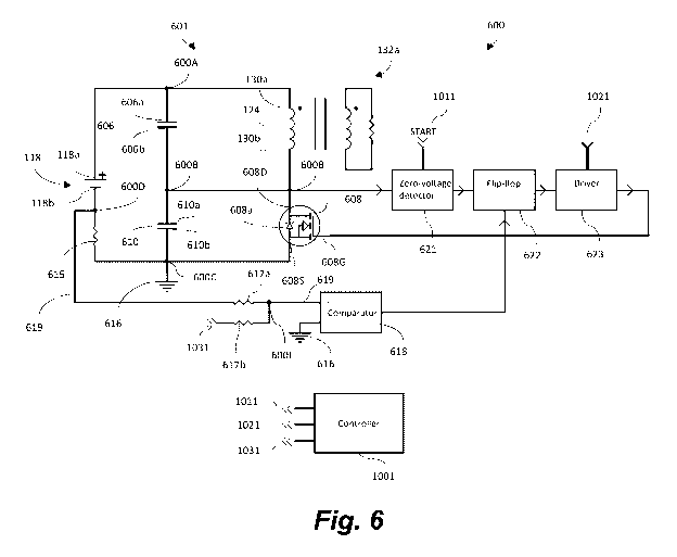
Now with reference to Figure 6, circuitry for induction heating by the device
100 will be described. Figure 6 shows a simplified schematic representation of
a part of
an induction heating circuit 600 of the aerosol generating device 100. Figure
6 shows a
part of the induction heating circuit 600 which comprises the first inductor
coil 124 for
heating the first susceptor zone 132a when a varying current flows through the
first
inductor coil 124. The first susceptor zone 132a is represented in Figure 6 as
having an
inductive element and a resistive element to represent how the susceptor 132
couples
inductively with the first inductor 124 and is heated through the generation
of eddy
currents. It will be noted that the device 100 additionally comprises the
second inductor
coil 126, which is not shown in Figure 6. The second inductor coil 126 is also
part of
the induction heating circuit 600 and is controlled to heat the second
susceptor zone
132b as will be described below. However, for the sake of clarity, the circuit
600 will
first be described with reference to those features shown in Figure 6.
The circuit 600 comprises a first resonator section 601, the DC voltage supply
118 for supplying a DC voltage to the first resonator section 601, as well as
a control
arrangement for controlling the circuit 600. The first resonator section 601
comprises
the first inductor 124 and a switching arrangement comprising a first FET 608,
and the
control arrangement is configured to switch the FET 608 between a first state
and a
second state in response to voltage conditions detected in the circuit 600, as
will be
described in more detail below, to operate the first inductor 124. The circuit
600, with
the exception of the susceptor 132, is arranged on the PCB 122 of the device
100, with
CA 03132764 2021-09-07
WO 2020/182731 PCT/EP2020/056220
the inductor coil 124 being connected to the PCB 122 at a first end 130a and a
second
end 130b.
The first resonator section 601 comprises a first capacitor 606, and a second
5 capacitor 610, both arranged in parallel with the first inductor 124 such
that when the
first resonator section 601 is allowed to resonate an alternating current
flows between
the first capacitor 606 and the second capacitor 610 and through the inductor
124. As
mentioned above, the first FET 608, in this example an n-channel MOSFET, is
arranged
to operate as a switching arrangement in the first resonator section 601.
It should be noted that in other examples, the resonator section 601 may
comprise only one capacitor, for example in the position of the first
capacitor 606, or at
the position of the second capacitor 610. In other examples, the resonator
section 601
may comprise any other number of capacitors, such as three or more capacitors.
For
example, either or both of the first capacitor 606 and the second capacitor
610 may be
replaced by two or more capacitors arranged in parallel with one another. As
will be
well understood, the resonator section 601 has a resonant frequency which is
dependent
on the inductance L and the capacitance C of the resonator section 601. The
number,
type and arrangement of capacitors in the resonating section 601 may be
selected based
on considerations of the power levels to be used in the circuit 600 and the
desired
frequency of operation of the circuit 600. For example, it will be understood
that
individual capacitors and an arrangement of said capacitors can be considered
to have
an equivalent series resistance (ESR) as well as a limit on the ability of
said capacitors
to handle current. Such features may be taken into account when determining an
arrangement of capacitors to provide the capacitance in the resonator section
601. For
example, depending on desired power levels and frequency of operation, there
may be
an advantage to providing a plurality of capacitors in parallel, to provide
higher
capacitance or lower ESR. In this example, the first and second capacitors
606, 610 are
both ceramic COG capacitors each having a capacitance of around 100nF. In
other
examples, other types of capacitor and/or capacitors with other capacitance
values, e.g.
capacitors with unequal capacitance values, may be used, according to the
considerations outlined in this paragraph.
CA 03132764 2021-09-07
WO 2020/182731 PCT/EP2020/056220
31
The first resonator section 601 is supplied a DC voltage by the DC voltage
supply 118, which is, for example, as described above, a voltage supplied by a
battery.
As shown in Figure 6, the DC voltage supply 118 comprises a positive terminal
118a
and a negative terminal 118b. In one example, the DC voltage supply 118
supplies a
DC voltage of around 4.2V to the first resonator section 601. In other
examples, the DC
voltage supply 118 may supply a voltage of 2 to 10V, or around 3 to 5V, for
example.
A controller 1001 is configured to control operation of the circuit 600. The
-- controller 1001 may comprise a micro-controller, e.g. a micro-processing
unit (VIPU),
comprising a plurality of inputs and outputs. In one example, the controller
1001 is an
STM32L051C8T6 model MPU. In some examples, the DC voltage supply 118
provided to the circuit 600 is provided by an output from the controller 1001
which
itself receives power from a battery or other power source.
The positive terminal 118a of the DC voltage source 118 is electrically
connected to a first node 600A. In an example, the DC voltage source 118 is
connected
to the node 600A via the controller 1001 which receives power from the DC
voltage
source 118 and supplies the voltage supplied by the DC voltage source to
components
of the device, including the circuit 600. The first node 600A is electrically
connected to
a first end 606a of the first capacitor 606 and to the first end 130a of the
first inductor
124. The second end 130b of the first inductor 124 is electrically connected
to a second
node 600B, which in Figure 6 is represented at two electrically equivalent
points in the
circuit diagram. The second node 600B is electrically connected to a drain
terminal
608D of the FET 608. In this example, the second node 600B is also
electrically
connected to a first end 610a of the second capacitor 610. Continuing around
the circuit,
the source terminal 608S of the first FET 608 is electrically connected to a
third node
600C. The third node 600C is electrically connected to ground 616, and in this
example
to a second end 610b of the second capacitor 610. The third node 600C is
electrically
connected via a current sense resistor 615 to a fourth node 600D, and the
fourth node
600D is electrically connected to the negative terminal 118b of the DC voltage
source
CA 03132764 2021-09-07
WO 2020/182731 PCT/EP2020/056220
32
118, which, as with the positive terminal, in an example is supplied via the
controller
1001.
It should be noted that in examples where the second capacitor 610 is not
present, the third node 600C may have only three electrical connections: to
the first FET
source terminal 608S, to ground 616 and to the current sense resistor 615.
As mentioned above, the first FET 608 acts a switching arrangement in the
first
resonator section 601. The first FET 608 is configurable between a first
state, i.e. an
.. 'ON' state and a second state, i.e. an 'OFF' state. As will be well
understood by those
skilled in the art when an n¨channel FET is in an OFF state (i.e. when the
appropriate
control voltage is not applied to its gate) it effectively acts as a diode. In
Figure 6, the
diode functionality that the first FET 608 exhibits when in its OFF state is
represented
by a first diode 608a. That is, when the FET 608 is in the OFF state the first
diode 608a
acts to largely prevent current flowing from the drain terminal 608D to the
source
terminal 608S but allows current to flow from the source terminal 608S to the
drain
terminal 608D if the diode 608a is appropriately forward biased. An n¨channel
FET is
in an ON state when an appropriate control voltage is applied to its gate so
that a
conductive path exists between its drain D and source S. As such, when the
first FET
608 is in the ON state, it acts like a closed switch in the first resonator
section 601.
As mentioned above, the circuit 600 may be considered to comprise a first
resonator section 601 and an additional control arrangement. The control
arrangement
comprises a comparator 618, a zero-voltage detector 621, and a flip-flop 622,
and is
configured to detect voltage conditions within the first resonator section 601
and to
control the first FET 608 in response to the detected voltage conditions. This
control of
the first FET 608 by the control arrangement will now be described in more
detail.
At the second node 600B there is electrically connected the zero-voltage
detector 621, which is configured to detect a voltage condition, i.e. a
voltage of at or
near OV with respect to a ground voltage, at a point in the circuit 600 to
which the zero-
voltage detector 621 is connected. The zero-voltage detector 621 is configured
to output
CA 03132764 2021-09-07
WO 2020/182731 PCT/EP2020/056220
33
a signal to control switching of the state of the FET 608. That is, the zero-
voltage
detector 621 is configured to output a signal to the flip-flop 622. The flip-
flop 622 is an
electrical circuit which is configurable between two stable states. The flip-
flop 622 is
electrically connected to a first gate driver 623 which is configured to
provide a voltage
to the first FET gate terminal 608G dependent on the state of the flip-flop.
That is, the
first gate driver 623 is configured to provide an appropriate voltage to the
first FET gate
terminal 608G to switch the FET 608 to the ON state when the flip-flop is in
one state,
but is configured not to provide a voltage appropriate for maintaining the FET
608 in
the ON state when the flip-flop 622 is in the other state. For example, the
first gate
.. driver 623 may be configured to provide an appropriate gate-source voltage
to the first
FET gate 608G to switch the FET 608 ON when the flip-flop 622 is in a state
'1', and
the first gate driver 623 may be configured not to provide the gate-source
voltage when
the flip-flop 622 is in state '0'. The state of the flip-flop means 622
therefore controls
whether the first FET 608 is on or off.
In this example, the zero-voltage detector 621 and the first gate driver 623
of
the control arrangement are configured to receive respective signals 1011,
1021 from
the controller 1001, by which signals the controller 1001 can initiate and
control
operation of the circuit 600, as will be discussed in more detail below.
At the fourth node 600D, there is electrically connected a control voltage
line
619. The control voltage line 619 is electrically connected to a fifth node
600E via a
resistor 617a and the fifth node 600E is electrically connected to the voltage
comparator
618 ¨ hereinafter comparator 618. The fifth node 600E is electrically
connected to a
positive terminal of the comparator 618. A negative terminal of the comparator
618 is
connected to ground 616. In this example, the comparator 618 is configured to
output a
signal based on a comparison of the voltage at the fifth node 600E to ground
voltage.
The output signal of the comparator 618 is sent to the flip-flop 622. A
control voltage
1031 is supplied, in this example from the controller 1001, to the control
voltage line
.. 619 via a second resistor 617b.
CA 03132764 2021-09-07
WO 2020/182731 PCT/EP2020/056220
34
As mentioned above, the comparator 618 is electrically connected to provide an
output to the flip-flop 622. The flip-flop 622 is configured such that an
output signal
from the comparator 618 can change the state of the flip-flop 622, and thereby
cause
the first driver 623 to change the state of the first FET 608.
The functioning of the example circuit 600 will now be described in more
detail
in the context of the first resonator section 601 being activated by the
controller 1001
such that the first inductor coil 124 is operated to heat the first susceptor
zone 132a.
To begin, the first FET 608 is configured in the OFF state, and is thus acting
as
a diode 608a, preventing current flowing through the inductor 124. The
controller 1001
initiates the operation of the circuit 600 to heat the first susceptor zone
132a by causing
the FET 608 to switch from the OFF state to the ON state. In this example the
controller
initiates operation of the circuit 600 by providing a START signal 1011 to the
zero-
voltage detector 621. The flip-flop 622 is thereby caused to change states and
cause the
first gate driver 623 to provide a signal to the FET gate terminal 608G to
thereby switch
the FET to the ON state.
Once the FET 608 is switched to the ON state, what may be referred to as a
self-
oscillating heating cycle of the circuit 600 begins. The FET 608, now being in
the ON
state, acts as a closed switch allowing a DC current to begin flowing from the
DC
voltage source positive terminal 118a through the first inductor 124 and
returning to the
DC voltage source negative terminal 118b via the current sense resistor 615.
The first
inductor 124 opposes this initial increase in current, as is well-known,
generating a back
emf via Faraday's and Lenz' s laws. In the ON state, the voltage between the
drain
terminal 608D and the source terminal 608S is substantially zero.
Figure 7A shows a schematic graphical representation of the current flowing
through the first inductor 124 against time t starting from when the FET 608
is switched
on, at time to. From time to, a DC current begins to build up in the inductor
124 from
zero at a rate which is dependent on an inductance Li of the inductor 124, a
DC
resistance of the circuit 600 and the DC supply voltage. In one example the
current
CA 03132764 2021-09-07
WO 2020/182731 PCT/EP2020/056220
sense resistor 615 has a resistance of around 2m0, while the inductor 124 has
a DC
resistance of, 2 to 15m0, or 4 to 10m12 or in this example around 5.2m0. This
build-
up of current in the inductor corresponds to the inductor 124 storing magnetic
energy,
and the amount of magnetic energy which can be stored by the inductor 124 is
5 dependent on its inductance Li, as will be well understood.
Figure 7B shows a simplified representation of the voltage across the current
sense resistor 615 against time t, again from the time to when the FET 608 is
turned on.
10 Shortly after the FET 608 is turned on, a voltage develops across the
inductor 124, this
being the back emf generated by the inductor 124 as the inductor opposes the
increase
in current. At this time, therefore, the voltage across the current sense
resistor 615 as
shown in Figure 7B is small, since almost all of the voltage difference
provided by the
DC supply 118 drops across the inductor 124. Then, as the current through the
inductor
15 124 increases and the back emf of the inductor 124 decays, the voltage
across the
current sense resistor 615 increases. This is seen as the development of a
negative
voltage across the current sense resistor 615, as shown in Figure 7B. That is,
the voltage
across the current sense resistor 615 becomes increasingly negative with the
length of
time that the FET 608 is on.
Since the increasingly negative voltage across the current sense resistor 615
corresponds with the increasing current through the inductor 124, the
magnitude of the
voltage across the current sense resistor 615 is indicative of the current
flowing through
the inductor 124. While the FET 608 remains on, the current through the
inductor 124
and the voltage across the current sense resistor 615 increase substantially
linearly
towards respective maximum values Lim, Vmax (which are dependent on the DC
voltage
supplied by DC supply 118 and the DC resistance of the circuit 600) with a
time
constant dependent on the inductance Li and on the DC resistance of the
circuit 600. It
should be noted that as the current through the inductor 124 is varying after
time to some
inductive heating of the susceptor 132 may occur while the DC current through
the first
inductor 124 builds up.
CA 03132764 2021-09-07
WO 2020/182731 PCT/EP2020/056220
36
The circuit 600 is configured such that the amount of energy which is stored
in
the first inductor 124 in the time during which the FET 608 is switched on, is
determined
by the control arrangement and can be controlled by the controller 1001. That
is, the
controller 1001 controls an amount of DC current (and thus an amount of
magnetic
energy) allowed to build up in the inductor 124, as will now be described.
As described above, the control voltage 1031 is applied to the control voltage
line 619. In this example, the control voltage 1031 is a positive voltage and
the voltage
input to the positive terminal of the comparator 618 (i.e. the voltage at the
fifth node
600E) at any one time is dependent on the value of control voltage 1031 and
the voltage
at the fourth node 600D. When the negative voltage across the current sense
resistor
615 reaches a particular value, it cancels, at the fifth node 600E, the
positive control
voltage 1031 and gives a voltage of OV (i.e. ground voltage) at the fifth node
600E. In
this example, the resistor 617a has a resistance of 21ca The resistor 617b
represents an
effective resistance to the controller 1001 of 70ka The voltage at the fifth
node 600E
reaches OV when the negative voltage across the current sense resistor 615 has
the same
magnitude as the control voltage 1031.
The comparator 618 is configured to compare the voltage at its positive
terminal
to the voltage of ground 616, connected to its negative terminal, and output a
signal as
a result. In one example the comparator is a standard component FAN156, as may
be
obtained from On-Semiconductor. Accordingly, when the voltage at fifth node
600E
reaches OV, the comparator 618 receives a OV signal at its positive terminal,
and the
result of the comparison by the comparator 618 is that the voltage at the
positive
terminal is equal to the voltage at the negative terminal. The comparator 618
consequently outputs a signal to the flip-flop 622 and causes the FET 608 to
be switched
off. As such, switching off of the FET 608 is dependent on a voltage condition
detected
in the circuit 600. Namely, in this example, when the comparator 618 detects
by
comparison of the voltage across its terminals that a negative voltage across
the current
sense resistor 615 has reached the same magnitude as the control voltage 1031,
which
CA 03132764 2021-09-07
WO 2020/182731 PCT/EP2020/056220
37
occurs at time ti, the FET 608 is switched off In Figure 7A, the DC current
flowing
through the inductor 124 at time ti when the FET 608 is switched off is
labelled
When the FET 608 is turned off, at time ti, the FET 608 switches from acting
like a closed switch to acting like a diode 608a in the resonator section 601,
and for the
purposes of supply from the DC supply 118 effectively acting like an open
switch. At
time ti the path of the DC current through the inductor 124 to ground 616 is
interrupted
by the FET 608. This triggers the current flowing in the first inductor 124 to
drop off
(this is not shown in Figure 7A), and the inductor 124 opposes this change in
current
by generating an induced voltage. Accordingly, current begins oscillating back
and
forth between the inductor 124 and the capacitors 606, 608 at the resonant
frequency of
the first resonator section 601.
Similarly, the voltage across the inductor 124 and thereby between the first
FET
drain 608D and source 608S terminals begins to oscillate at the resonant
frequency of
the first resonator section 601. As the current through and voltage across the
inductor
124 begin to oscillate, the susceptor 132 is inductively heated. Switching the
FET 608
to the OFF state, therefore acts to release the magnetic energy stored in the
inductor
124 at time ti to heat the susceptor 132.
Figure 8 shows a trace 800 of the voltage across the first FET 608, starting
from
the FET 608 being in the ON state from time to to ti. Over the time
illustrated in Figure
8 the first FET 608 is turned off and on twice.
The voltage trace 800 comprises a first section 800a between times to and ti
when the first FET 608 is ON, and a second section 800b to 800d when the first
FET
608 is switched off. At 800e the FET 608 is switched on again, and a third
section 800f
which is equivalent to the first section 800a begins while the first FET 608
remains on
and the above-described process of building up of DC current through the
inductor 124
repeats. Figure 8 also shows a fourth section 800g when the first FET 608 is
switched
off again to allow oscillation of the voltage across the FET 608, and a fifth
section 800h
when the first FET 608 is subsequently switched on again.
CA 03132764 2021-09-07
WO 2020/182731 PCT/EP2020/056220
38
The voltage across the first FET 608 is zero when the first FET 608 is on in
sections 800a, 800f and 800h. When the first FET 608 is turned off as
indicated by
section 800b to 800d and also by section 800g, the first inductor 124 uses the
energy
stored in its magnetic field (which magnetic field was the result of the DC
current built
up when the first FET 608 was on) to induce a voltage that opposes a drop in
the current
flowing through the first inductor 124 as a result of the first FET 608 being
off The
voltage induced in the first inductor 124 causes a corresponding variation in
voltage
across the first FET 608. During this variation in voltage, the first inductor
124 and the
capacitors 606, 610 begin to resonate with each other with a sinusoidal
waveform. The
voltage shown by voltage trace 800 initially increases (see for example 800b)
as the
induced voltage in the first inductor 124 increases to oppose a drop in
current due to
the first FET 608 being off, reaches a peak (see for example 800c) and then,
as the
energy stored in the magnetic field of the first inductor 124 diminishes,
decreases back
to zero (see for example 800d).
The varying voltage 800b to 800d and 800g produces a corresponding varying
current (not shown) and, since during the off time of the first FET 608, the
capacitors
606, 610 and the first inductor 124 act as a resonant LC circuit, the total
impedance of
the combination of the first inductor 124 and capacitors 606, 610 is at a
minimum during
this time. It will therefore be understood that the maximum magnitude of the
varying
current flowing through the first inductor 124 will be relatively large. This
relatively
large varying current accordingly causes a relatively large varying magnetic
field in the
first inductor 124 which causes the susceptor 132 to generate heat. The time
period over
which the voltage across the first FET 608 varies as indicated by section 800b
to 800d
and by section 800g in this example depends on the resonant frequency of the
first
resonator section 601.
Referring now to Figures 6 and Figure 8, the circuit 600 is configured such
that
when the first FET 608 is off and the voltage across the first FET 608
decreases back
towards OV, the zero-voltage detector 621 detects this voltage condition and
outputs a
signal to the flip-flop 622 which causes the first FET 608 to be switched back
to the
ON state. That is, in response to this voltage condition detected within the
first resonator
CA 03132764 2021-09-07
WO 2020/182731 PCT/EP2020/056220
39
section 601, the FET 608 is switched from the OFF state to the ON state. The
zero-
voltage detector 621 may be considered to detect a voltage condition
indicative that a
given proportion of a cycle of current oscillation between the inductive
element and the
capacitive element has been completed since the FET 608 was switched off That
is, the
zero-voltage detector 621 detects that a half-cycle of current (and voltage)
oscillation
at the resonant frequency of the first resonator section 601 has been
completed by the
zero-voltage detector 621 detecting that the voltage across the FET 608 has
returned to
OV or nearly OV.
In some examples, the zero-voltage detector 621 may detect when the voltage
across the first FET 608 has returned to at or below a voltage level 801 and
as such may
output a signal to cause switching of the state of the FET 608 before the
voltage across
the FET 608 reaches exactly OV. As is illustrated by Figure 8, the operation
of the zero-
voltage detector 621 curtails oscillations of the voltage in the resonator
section 601 after
one half-cycle and thus results in a substantially half-sine wave voltage
profile across
the first FET 608. Further details of the operation of the zero-voltage
detector 621 will
be described below with reference to Figure 9.
When the first FET 608 is switched back on, at point 800e, a DC current driven
by the DC source 118 again builds up through the first inductor 124. The first
inductor
124 may then again store energy in the form of a magnetic field to be released
when the
first FET 608 is next switched off to initiate resonance within the first
resonator section
601. As the first FET 608 is repeatedly switched on and off in this way, the
above
described process is continuously repeated to heat the susceptor 132.
It should be noted that the above described building up of current through the
inductor 124 described with reference to Figures 7A and 7B occurs both when
the FET
608 is turned on initially in response to a START signal 1011 from the
controller 1001
and when the FET 608 is switched on subsequently by a zero-voltage condition
detected
by the zero-voltage detector 621. In the first instance, in response to the
START signal
1011, the current in the inductor 124 builds up substantially linearly from 0.
In the
second instance, when the FET 608 is turned back on in response to a detected
zero
CA 03132764 2021-09-07
WO 2020/182731 PCT/EP2020/056220
voltage condition at point 800e, some excess current is circulating in the
circuit 600
(e.g. from previous cycles of switching on and off of the FET 608). As the FET
608 is
turned back on following the detection of a zero-voltage condition, the
recirculating
current produces an initial negative current through the FET 608. Then, while
the FET
5 608 remains on, the current through the FET 608 and inductor 124 builds
up,
substantially linearly, from the initial negative current value produced by
the
recirculating current. As the current through the inductor 124 builds up, the
voltage
across the current sense resistor 615 correspondingly becomes increasingly
negative, in
the manner described above.
In examples, switching on and off of the FET 608 may occur at a frequency of
around 100kHz to 2MHz, or around 500kHz to 1MHz, or around 300kHz. The
frequency at which the switching on and off of the FET 608 occurs is dependent
upon
the inductance L, the capacitance C, the DC supply voltage supplied by the
supply 618
and further upon a degree to which current continues recirculating through the
resonator
section 601 and the loading effect of the susceptor 132. For example, where
the DC
supply voltage equals 3.6V, the inductance of the inductor 124 is 140nH, and
the
capacitance of the resonator section 601 is 100nF, the time for which the FET
608
remains on may be around 2700ns and the time for a half-cycle of oscillation
to
complete when the FET 608 is off may be around 675ns. These values correspond
to a
power of around 20W being supplied from the DC voltage supply 118 to the
resonator
section 601. The above value of the time for which the FET 608 remains on is
affected
by the amount of current which recirculates in the circuit, since as described
above, this
recirculating current causes an initial negative current through the inductor
upon
switching on of the FET 608. It should also be noted that the time for the
current to
build up to the value which causes switching off of the FET 608 is also at
least in part
dependent on the resistance of the inductor 124, however, this has a
relatively minor
effect on the time when compared to the effect of the inductance of the
resonator section
601. The time for a half-cycle of oscillation to complete (of in this example
675n5) is
dependent on the resonant frequency of the resonator section 601 which is
affected not
only by the values of inductance and capacitance of the inductor 124 and
capacitors
CA 03132764 2021-09-07
WO 2020/182731 PCT/EP2020/056220
41
606, 610 respectively, but also by the effective resistance provided by
loading the
inductor 124 with the susceptor 132.
Thus far, the circuit 600 has been described in terms of its operation to heat
the
susceptor 132 by one inductor, the first inductor 124, and thus only a part of
the circuit
600 used by the device 100 has been described. However, as described above,
the device
100 also comprises a second inductor 126 for heating the second zone 132b of
the
susceptor 132. Figure 9 shows a simplified schematic of the circuit 600
comprising the
second inductor 126 in addition to the first inductor 124.
As shown in Figure 9, in addition to the features described with reference to
Figures 6 to 8, the circuit 600 comprises a second resonator section 701
comprising the
second inductor coil 126, a third capacitor 706, a fourth capacitor 710 and a
second
FET 708, having a drain terminal 708D, a source terminal 708S, and a gate
terminal
708G. Additionally, the circuit 600 comprises a second gate driver 723
configured to
provide a gate-source voltage to the second FET gate terminal 708G. The
controller
1001 is not shown in Figure 9 but the controller 1001 controls the circuit 600
in the
manner described with reference to Figures 6 to 8 and additionally is
configured to
provide a control signal 1012 to the second gate driver 723. Some reference
numerals
of features of the circuit 600 already described with reference to Figure 6
have been
omitted from Figure 9 for the sake of clarity.
As described above, the first inductor 124 is arranged to heat the first zone
132a
of the susceptor 132 and the second inductor 126 is arranged to heat the
second zone
132b of the susceptor 132. The second inductor 126, third and fourth
capacitors 706,
710, and second FET 708 are arranged to form the second resonator section 701,
in the
same manner as the first inductor 124, first and second capacitors 606, 610,
and first
FET 608 are arranged to form the first resonator section 601. In one example,
the third
and fourth capacitors 706, 710 are also COG capacitors and may have a
capacitance of
around 100nF. The second inductor 126 in one example has a DC resistance of
around
8maWhen active, the second resonator section 701 operates to heat the
susceptor 132
CA 03132764 2021-09-07
WO 2020/182731 PCT/EP2020/056220
42
in an equivalent manner as described above for the first resonator section 601
and
description of this will not be repeated here.
It will be appreciated that the value of the DC resistance of the inductors
124,
126 will have an effect on the efficiency of the circuit 600, since a higher
DC resistance
will result in higher resistive losses in the inductor 124, 126 and as such it
may be
desirable to minimise inductor DC resistance, for example by changing the
number of
windings, or the cross-section of the inductors 124, 126. Furthermore, it will
be
appreciated that an AC resistance of the inductor 124 is increased compared to
the DC
resistance due to the skin effect. As such, the use of Litz wire in examples
provides for
reducing the skin effect, and thereby reducing AC resistance and associated
resistive
losses from the inductors 124, 126. To give an example, where the first
inductor 124
has a DC resistance of around 5mS2 and the second inductor 126 has a DC
resistance of
around 8m, and the circuit operates at around 300kHz, the particular
arrangement of
Litz wire forming the coils results in effective resistances for the inductors
124, 126 of
around 1.14 times their DC resistance values.
A node 700A in the second resonator section 701 is equivalent to the first
node
600A of the first resonator section 601 and is electrically connected to the
first node
600A and thereby to the positive terminal 118a of the DC supply 118. A node
700C is
at the equivalent position in the second resonator section 701 as is the third
node 600C
of the first resonator section 601 and the node 700C is similarly connected to
ground
616.
It is important to note that the circuit 600 is configured to be operated by
the
controller 1001 such that only one of the resonator sections 601, 701 is
active at any
one time. Examples of this operation will be described in more detail below.
During the activation of one of the resonator sections 601, 701, the zero-
voltage
detector 621 is configured to detect a zero-voltage condition in the active
resonator
section 601, 701 and thus control switching of the respective FET 608, 708 of
the active
resonator section 601, 701. The zero-voltage detector 621 controls when the
respective
CA 03132764 2021-09-07
WO 2020/182731 PCT/EP2020/056220
43
FET 608, 708 of the active resonator section 601, 701, is switched back on
(such as at
point 800e), and example of this will now be described in more detail, with
reference
to Figures 8 to 10.
In the circuit 600, the zero-voltage detector 621 is configured to detect a
zero-
voltage condition at the second node 600B of the first resonator section 601
or at the
equivalent node 700B of the second resonator section 701. When one of the
first
resonator section 601 and second resonator section 701 is active, the zero-
voltage
detector 621 detects each time the respective FET 608, 708 has been switched
off, that
the voltage across that FET 608, 708 has returned to zero (e.g. point 800e in
Figure 8)
or, is close to zero e.g. below a level 801. In response to the zero-voltage
detector 621
making this detection, a signal is output to change the state of the flip-flop
622. The
respective gate driver 623 which is in operation then outputs a gate-source
voltage to
switch the respective FET back to the ON state.
A first small signal diode 725 connects the zero-voltage detector 621 to the
first
resonator section second node 600B and a second small signal diode 726
connects the
zero-voltage detector 621 to the equivalent node 700B of the second resonator
section
701. Specifically, anodes of the first small signal diode 725 and second small
signal
diodes are connected to the zero-voltage detector 621 input via a common node
701B
while cathodes of the diodes 725, 726 are connected respectively to the nodes
600B,
700B.
The operation of the zero-voltage detector 621, in a particular example, will
now
be described with reference to Figure 10, which shows the zero-voltage
detector 621
and the flip-flop 622. In Figure 10, the components which make up the zero-
voltage
detector 621 are enclosed by a dotted line box. The node 701B connected to the
anodes
of the first and second small signal diodes 725, 726 is shown. The start
signal 1011
from the controller 1001 to the zero-voltage detector 621 can also be seen in
Figure 13.
The zero-voltage detector 621 in this example comprises an inverter gate U103
having an input 2 from the node 701B and an output 4 connected to an input of
the flip-
CA 03132764 2021-09-07
WO 2020/182731 PCT/EP2020/056220
44
flop 622. The inverter gate U103 is powered by connections 5 and 3 and a
capacitor
C108 isolates the connection 5 from ground. A logic power supply 621a of, in
this
example, 2.5V is applied to the input 5 and via a pull-up resistor R111 to the
input 2 of
the inverter gate U103. The logic power supply 621a is in this example
supplied from
the controller 1001. The inverter gate U103 is configured to act as an OR gate
for the
START signal 1011 and a zero-voltage detection signal from the node 701B. That
is,
the inverter gate U103 is configured to receive a logic low signal in the form
of the
START signal 1011 from the controller 1001 to initiate operation of the
circuit 600a.
The START signal 1011 may be provided by on "open drain" signal pin of the
controller
1001. The inverter gate U103 is also configured to receive a logic low signal
from the
node 701B when one of the first and second signal diodes 725, 726 is forward
biased
due to one of the nodes 600B, 700B being at or near zero volts, as will be
explained
below. When either or both of these logic low signals is received by the
inverter gate
input 2 the inverter gate U103 inverts the received signal and outputs a logic-
high signal
to the flip-flop 622.
When the first inductor 124 is being operated to heat the susceptor 132, the
second FET 708 remains off. When the second FET 708 remains off, the second
small
signal diode 726 has either no bias or is reverse biased depending on the
voltages at the
logic power source and the DC supply 118, that is, the voltage at a cathode
end (nearest
the node 700B) of the second small signal diode 726 is either substantially
the same as
or higher than the voltage at an anode end (nearest the zero-voltage detector
621) of the
second small signal diode 726.
During operation of the first resonator section 601, when the first FET 608 is
off and the voltage across it varies as indicated by 800b-d of Figure 8, the
first small
signal diode 725 is reverse biased. At the end of this variation in voltage,
when the
voltage reaches OV as indicated by 800e, or is close to OV (e.g. at or below
level 801),
the first small signal diode 725 becomes forward biased. Accordingly, when the
first
small signal diode 725 is forward biased at 800e, the signal provided to the
input 2 of
the inverter gate U103 becomes a logic low signal since a voltage drop is
produced from
the logic signal 621a across the resistor R111.As such, once this logic low
signal is
CA 03132764 2021-09-07
WO 2020/182731 PCT/EP2020/056220
inverted by the inverter gate U103, a logic high signal is provided at the
output 4 of the
inverter gate U103.
Although in the above description the functioning of the zero-voltage detector
5 621 is
described in relation to controlling switching of the first FET 608, it will
be
understood that the zero-voltage detector 621 functions in the same way, using
the
second small signal diode 726 instead of the first small signal diode 725, to
control the
second FET 708.
10 Still
with reference to Figure 10, the flip-flop 622 comprises a clock input CLK,
a reset input /RST, and an output Q. The flip-flop 622 also comprises further
inputs D
and VCC for supplying power, in this example the flip-flop receives the same
2.5V
logic power supply 621a from the controller 1001 as the inverter gate U103
receives.
The clock input CLK is connected to the output 4 of the inverter gate U103 and
is
15
configured to receive a signal therefrom. When the output 4 of the inverter
gate U103
switches from logic-low to logic-high (due to the input 2 of inverter gate
U103 receiving
a detected zero-voltage condition or a START signal 1011 as described above)
the clock
input CLK of the flip-flop 622 receives a logic-high rising edge signal which
"clocks"
the flip-flop 622 and makes the state of the flip-flop output Q high. The flip-
flop 622
20
comprises a further input /RST configured to receive a signal from the output
of the
comparator 618, by which the comparator 618 can change the state of the flip-
flop 621
to cause the flip-flop output Q to be low. The flip-flop output Q is connected
to the first
and second gate drivers 623, 723 and on receiving a high output from the flip-
flop
output Q, whichever one of the gate drivers 623, 723 is active (due to
receiving a signal
25 1021,
1022 as described above) provides a gate driver signal to its respective FET
608,
708.
In one particular example, the flip-flop 622 may switch at half of the voltage
of
the logic power source 621a, that is, at 1.25V in this example. This means
that the
30 forward
bias voltage of the first small signal diode 725 and the voltage at the first
FET
drain 608D must sum to 1.25V in order that the first FET 608 is switched on.
In this
example therefore, the first FET 608 is switched on when its drain 608D is at
0.55V
CA 03132764 2021-09-07
WO 2020/182731 PCT/EP2020/056220
46
rather than at exactly OV. It should be noted that ideally, switching may
occur at OV
across the FET 608 for maximum efficiency.
This zero-voltage switching
advantageously prevents the first FET 608 from discharging the capacitors 606,
610
and thereby wasting energy stored in said capacitors 606, 610.
Figure 11 shows in more detail the first and second gate drivers 623, 723 and
their connection to the gates 608G, 708G of their respective FETs 608, 708.
Each of
the gate drivers 623, 723 has an input IN which is configured to receive a
signal
dependent on the heater activation signals 1021, 1022 supplied from the
controller
1001. Additionally, the signals received by the inputs IN of the gate drivers
623, 723
are dependent on whether the signal output by the flip-flop output Q is high.
The inputs
IN are connected to the output Q of the flip-flop 622 via respective resistors
R125,
R128, which in this example each have a value of 21ca
The gate drivers 623, 723 each have two further inputs VDD and XREF wherein
each input VDD receives a 6V power supply from the controller 1001 and XREF
receives a 2.5V logic voltage, which in this example is the same logic voltage
supplied
by the controller 1001 to the flip-flop 622 and inverter gate U103. The inputs
VDD of
each of the first and second gate drivers 623, 723 are connected to a 6V
supply voltage
and the inputs VDD are connected to ground via two buffering capacitors C120,
C121.
The gate drivers 623, 723 also each have a terminal GND connected to ground
wherein
the terminals VDD and GND act to supply power to the gate drivers 623, 723. In
this
example, the capacitors C120, C121 each have a value of 1 .F. The gate drivers
623,
723 are configured to output gate drive voltages from respective outputs OUT.
The
outputs OUT of the gate drivers 623, 723 are connected respectively to FET
gates 608G,
708G via resistors R114, R115, which in this example each have a resistance of
4.99Q.
Each gate driver 623, 723 is configured to receive a signal at its input IN to
cause the gate driver to be activated only while a logic-high signal is
provided from the
flip-flop output Q and a heater activation signal 1021, 1022 is received from
the
controller 1001. An "open-drain" signal pin may be provided on the controller
1001
which is configured to provide the signals 1021, 1022.
CA 03132764 2021-09-07
WO 2020/182731 PCT/EP2020/056220
47
In examples, initiation of the circuit 600 for heating by one of the resonator
sections 601, 701 proceeds by the controller 1001 first initiating the desired
one of the
gate drivers 623, 723 by a respective one of the heater initiation signals
1021, 1022.
The controller 1001 then supplies the START signal 1011 to the zero-voltage
detector
621. The duration of the START signal 1011 should be shorter than the period
of half
a cycle of oscillation by the active resonator section 601, 701 (this period
may be
referred to as the "resonant fly-back period"). This allows the circuit to
properly begin
self-oscillating in response to a detected zero-voltage condition. In another
example,
the order the START signal 1011 and respective heater enable signal 1021, 1022
may
be reversed such that the START signal 1011 is first applied to set the flip-
flop Q output
to high, and one of the heater initiation signal 1021, 1022 then applied to
begin the self-
oscillating of the resonator section 601, 701 corresponding to heater to which
the signal
1021, 1022 is supplied.
To continue with describing in more detail the control arrangement for
controlling the circuit 600, Figure 12 shows a portion of the control
arrangement
comprising the comparator 618 and associated components. In Figure 12, the
positive
terminal 118a of the DC power supply 118 is shown connecting to a node 1500A
which
is connected to nodes 600A, 700A of the first and second resonator sections
601, 701
respectively. The negative terminal 118b of the DC power supply is connected
to a node
1500B which is equivalent to the node 600D shown in Figure 6. The node 1500B
connects to ground 616 via the current sense resistor 615. Between the nodes
1500A
and 1500B an arrangement of capacitors C111, C112, C115 and C116, each in this
example having a capacitance of 100 F, are connected in parallel, providing
buffering
between nodes 1500A and 1500B.
Figure 12 shows in more detail components associated with the functioning of
the comparator 618 for detecting that the current through the active inductor
124 or 126
has reached a given level. As described with reference to earlier figures, the
comparator
618 acts to compare a voltage indicative of an amount of DC current flowing in
the
active inductor (124 or 126) to a control voltage 1031 originating from the
controller
CA 03132764 2021-09-07
WO 2020/182731 PCT/EP2020/056220
48
1001. The comparator 618 receives power via an input 6 which is connected via
a 100S2
resistor R116 to a 2.5V logic power signal, in this example supplied by the
controller
1001 and the same logic signal as the signal 621a received by the flip-flop
622. The
comparator power input 6 is connected to ground via a lOnF capacitor C119. A
further
terminal 2 of the comparator 618 is connected directly to ground.
In some examples, the controller 1001 is a micro-processing unit comprising a
timer (not shown) for generating a signal which produces the control voltage
1031. In
this example, the control voltage 1031 is produced by a pulse-width modulated
signal
PWM DAC generated by the controller 1001. The timer of the controller 1001
generates a pulse-width modulated square waveform, with, for example, a
magnitude
of around 2.5V and a frequency of around 20kHz and having a particular duty
cycle.
The pulse-width modulated signal PWM DAC is filtered by lOnF capacitors C127
and
C128, and by two 49.9kS2 resistors R121, R123 and a 10kS2 resistor R124 to
provide a
substantially constant control voltage 1031 at the frequency at which the
controller 1001
controls the control voltage 1031 (of, e.g., around 64Hz in examples). To
adjust the
control voltage 1031, the controller 1001 in examples is configured to adjust
the duty
cycle of the pulse-width modulated signal PWM DAC applied to the circuit 600.
As
such, the components positioned between the input PWM DAC and the positive
terminal of the comparator 618 effectively provide for the control voltage
1031 to be
produced by a pulse-wave modulated signal and for the control voltage 1031
magnitude
to be adjusted by adjusting the duty cycle of this pulse wave modulated
signal. The
control voltage line 619 shown in Figures 6 and 9 may thus be replaced by
these
components. However, in other examples, the control voltage 1031 may produced
by a
substantially constant voltage supplied, for example, by the controller 1001.
In such
examples, some or all of the components for shown in Figure 12 for filtering
the signal
PWM DAC may not be present.
The node 1500B which is input to the comparator 618 positive input is, as
mentioned above, equivalent to the node 600D of the circuit 600. It can be
seen from
Figure 12 that, as described with reference to the simplified schematic shown
in Figure
6, the node 1500B is connected via the resistor 617a to the positive input of
the
CA 03132764 2021-09-07
WO 2020/182731 PCT/EP2020/056220
49
comparator 618. As such, the operation of the comparator 618 is as described
above: to
receive an input at its positive terminal which is dependent on the control
voltage 1031
and the voltage across the current sense resistor 615. When the voltage at the
positive
terminal of the comparator 618 reaches ground voltage, a signal /FF RST is
output, via
a resistor R118, to the flip-flop 622 input /RST to change the state of the
flip-flop 622
and thereby switch the active FET 608/708 off.
Figure 13 shows further components for a particular example of the control
arrangement for the circuit 600. The components shown in Figure 13 define
current
sense apparatus 1300 for providing a signal I SENSE indicative of an amount of
current
drawn from the DC voltage supply 118 during operation of the circuit 600. From
this
signal, the controller 1001 may determine a current drawn from the voltage
supply 118,
and may use this along with a value of the voltage supplied by the DC voltage
supply
118 to determine a value for a power supplied to the circuit 600. In some
examples, as
will be described below, a determined value of power may be used by the
controller
1001 for controlling the circuit 600.
An input 1301 to the current sense apparatus 1300 is provided via the resistor
R120 shown in Figure 12. The input is therefore connected to the node 1500B
via the
resistor R120 and receives a voltage indicative of the voltage across the
current sense
resistor 615. The current sense apparatus 1300 operates as a low-side current
sensing
apparatus for the circuit 600. In that regard, the current sense apparatus
1300 comprises
an op-amp U110 running on a voltage of 3.8V supplied to an input 5 of the op-
amp
U110 (component type TS507) set up for low-side current sensing using the
current
sense resistor 615, as will be well understood. A transistor U109 with built-
in bias
resistor (component type RN4986) acts to switch a 2.5V supplied by the
controller 1001
up to the 3.8V supply for the op-amp U110. The power supply line from the
transistor
component U109 is connected to ground via a lOnF capacitor C132. Further, a
11cS2
resistor R130 is connected between the positive input of the op-amp U110 and
ground
and a 4121cS2 resistor R129 is connected between the 2.5V input from the
controller
1001 and the positive input of the comparator U110. The negative terminal of
the op-
amp U110 receives a voltage dependent on the voltage across the current sense
resistor
CA 03132764 2021-09-07
WO 2020/182731 PCT/EP2020/056220
615. A resistor R131 and capacitor C133 in series provide filtering of the
voltage signal
received via the input 1301. A further resistor R133 (in this example having
resistance
of 97.6kS2) and a 1 OnF capacitor C134 are connected in parallel between the
input to
the negative terminal of the op-amp U110 and the output of the op-amp U110
such that
5 op-amp operates in a closed-loop mode.
The position of the current sense resistor 615, which, as mentioned above, in
one example is a 2mS2 resistor, in the circuit allows for a plurality of
parameters to be
measured with one current sense resistor, which may allow for good efficiency.
That is,
10 the position of the current sense resistor 615 in the circuit allows
measurement of: the
FET peak current, which may be used, for example, in control of the induction
heating
power of the circuit; the average current out of the battery, which may be
used in
monitoring discharge of the battery and setting the induction power; and the
average
current into the battery, which may be used, for example, in monitoring
charging of the
15 battery.
The op-amp U110 operates to output a voltage signal I SENSE to the controller
1001 which is indicative of the current through the current sense resistor 615
and thus
allows the controller 1001 to determine the current drawn from the DC voltage
supply
20 118 through the circuit 600.
It should be noted that having regard to the first and second FETs 608 and
708,
and the topology of the circuit 600, the phasing of the first and second
inductor coils
124 and 126 with respect to each other may be chosen such that when the first
inductor
25 coil 124 is being operated, current sufficient to cause significant
heating of the susceptor
132 is prevented from flowing in the second inductor coil 126, and when the
second
inductor coil 126 is being operated, current sufficient to cause significant
heating of the
susceptor 132 is prevented from flowing in the first inductor coil 124.
30 As described above, the first 608 and second 708 FETs effectively act
as diodes
608a, 708a when switched off and so may conduct a current if they are forward
biased
(i.e. the FETs are not perfect switches). Accordingly, in examples the circuit
600 may
CA 03132764 2021-09-07
WO 2020/182731 PCT/EP2020/056220
51
be configured so that when one of the first 124 and 126 inductor coils is
active to heat
the susceptor 132, the voltage induced across the other inactive inductor coil
does not
forward bias the intrinsic diode of the FET associated with that inactive
inductor coil
but instead reverse biases it.
The effect of the above described control arrangement being configured to
control the switching arrangements 608, 708 of the circuit 600 in response to
detected
voltage conditions is that when one of the first resonator section 601 and the
second
resonator section 701 is active (i.e. its gate driver 623, 723 is activated by
the controller
1001) that resonator section "self-oscillates", while the other section
remains inactive.
That is, switching of the respective FET 608, 708 in the resonator section
601, 701
repeats at a high frequency as a first voltage condition (detected by the
comparator 618)
causes the FET to be switched from on to off, and a second voltage condition
(detected
by the zero-voltage detector 621) causes the FET to be switched from off to
on.
The controller 1001 is configured to control the induction heating circuit 600
of
the device 100 such that only one of the first inductor 124 and the second
inductor 126
is active at any one time. The controller 1001 is configured to determine at a
pre-
determined frequency which of the first inductor 124 and the second inductor
126 to
activate.
In examples, during usage of the device 100 the controller 1001 determines at
the pre-determined frequency, i.e. one time for each of a plurality of pre-
determined
time intervals, which of the first resonator section 601 and the second
resonator section
701 to activate. In one example, each time the controller 1001 determines
which of the
first resonator section 601 and the second resonator section 701 to activate,
the
controller 1001 may determine to activate that resonator section to heat the
susceptor
132 for the duration of the next pre-determined interval. That is, where the
pre-
determined frequency (which may be referred to as an "interrupt rate") is
64Hz, for
example, the controller 1001 may determine at pre-determined intervals of
1/64s, which
resonator section 601, 701 to activate for a following duration of 1/64s until
the
controller makes the next determination of which resonator section 601, 701,
at the end
CA 03132764 2021-09-07
WO 2020/182731 PCT/EP2020/056220
52
of the following 1/64s interval. In other examples, the interrupt rate may be,
for
example, from 20Hz to 80Hz, or correspondingly the pre-determined intervals
may be
of length 1/80s to 1/20s. In order to determine which inductor 124, 126 is to
be activated
for a pre-determined interval, the controller 1001 determines which susceptor
zone
132a, 132b should be heated for that pre-determined interval. In examples, the
controller 1001 determines which susceptor zone 132a, 132b should be heated
with
reference to a measured temperature of the susceptor zones 132a, 132b, as will
be
described below.
Figure 14 shows a flowchart representation of an example method of
determining which of the two resonator sections 601, 701, should be activated
for a
particular pre-determined interval. In this example, the controller 1001,
determines
which of the first 601 and second 701 resonator sections to activate for the
pre-
determined interval based on a present temperature Ti of the first susceptor
zone 132a
heated by the first inductor 124 and a present temperature T2 of a second
susceptor
zone 132b heated by the second inductor 126. In an example, the present
temperatures
Ti and T2 of the first 132a and second 132b susceptor zones may be measured by
respective thermocouples (not shown) attached to each zone of the susceptor
132. The
thermocouples provide an input to the controller 1001 allowing the controller
1001 to
determine the temperatures Ti, T2. In other examples, other suitable means may
be
used to determine the respective temperatures of the susceptor zones 132a,
132b.
At block 1051, the controller 1001 determines a present value of the
temperature
Ti and compares this to a target temperature targetl for the first zone 132a
arranged to
be heated by the first inductor 124. The target temperature targetl of the
first zone 132a
has a value which may vary throughout a usage session of the device employing
the
circuit 600. For example, a temperature profile may be defined for the first
zone
defining values for targetl throughout a usage session of the device 100.
At block 1052 the controller 1001 performs the same operation as was
performed for the first inductor 124 at block 1051 and determines whether the
present
temperature T2 of the second zone 132b is below the target temperature target2
for the
CA 03132764 2021-09-07
WO 2020/182731 PCT/EP2020/056220
53
second zone 132b at this time. Again, the target temperature of the second
zone 132b
may be defined by a temperature profile defining values of target2 throughout
a usage
session. The temperature of the second zone 132b may, similarly to the first
zone 132a,
be measured by any suitable means such as by a thermocouple.
If the answers at block 1051 and block 1052 are both "no", i.e. both susceptor
zones 132a, 132b are presently at or above their respective target
temperatures targetl,
target2, then the controller 1001 determines neither of the first and second
resonator
sections 601, 701 should be activated for the next pre-determined interval.
If the answer at block 1051 is "no" and the answer at block 1052 is "yes",
i.e.
the first zone 132a is at or above its target temperature targetl but the
second zone 132b
is below its target temperature target2, then the controller 1001 determines
that the
second resonator section 701 should be activated to heat the second zone 132b
for the
next pre-determined interval.
If the answer at block 1051 is "yes" and the answer at block 1052 is "no",
i.e.
the first zone 132a is below its target temperature targetl and the second
zone 132b is
at or above its target temperature target2, then the controller 1001
determines that the
first resonator section 601 should be activated to heat the first zone 132a
for the next
pre-determined interval.
If the answer at block 1051 is "yes" and the answer at block 1052 is "yes",
i.e.
both the first 132a and second 132b zones are below their respective target
temperatures
targetl, target2, then the controller 1001 continues to block 1053. At block
1053 the
controller 1001 effectively acts to alternate activation of the first
resonator section 601
and second resonator section 701 for each pre-determined interval that both
zones 132a,
132b remain below their respective target temperatures.
In one example, in order to alternately activate the first 601 and second 701
resonator sections, at block 1053 the controller 1001, in some examples,
determines if
an even number of predetermined intervals has elapsed since the start of the
session. If
CA 03132764 2021-09-07
WO 2020/182731 PCT/EP2020/056220
54
an even number of predetermined intervals has elapsed since the start of the
session
then the controller 1001 determines that the first resonator section 601
should be
activated for the next interval. If an odd number of predetermined intervals
has elapsed
since the start of the session then the controller 1001 determines that the
second
resonator section 701 should be activated for the next interval. In other
examples, it
should be understood, that the controller 1001 may instead activate the second
resonator
section 701 when an even number of intervals has elapsed and the first
resonator section
601 when an odd number of intervals has elapsed.
In certain examples, the circuit 600 is configured such that once one of the
resonator sections 601, 701 is activated by receipt of a signal 1021 or 1022
at one of
the gate drivers 623, 624, the that resonator section 601/701 continues to
operate, i.e.
self-oscillate, until deactivated by the controller 1001, for example by
providing a
different signal to the gate driver of that resonator section 601/701. As
such, upon
determining which of the resonator sections 601, 701 to activate during a
given interval,
the controller 1001, in order to initiate this activation may deactivate one
of the
resonator sections 601, 701 which was active during a previous interval.
To illustrate an example of block 1053 where method 1050 shown in Figure 14
is performed with intervals of 1/64s, if the controller 1001 determines that
both zones
132a, 132b are below their respective target temperatures targetl, target2 and
an even
number of 1/64s intervals has elapsed since the start of the usage session of
the device
100, then the controller 1001 activates the first resonator section 601 for
the next 1/64s
interval while the second resonator section 701 is rendered inactive, which in
examples
requires the controller 1001 deactivating the second resonator section 701. If
after this
next interval of 1/64s both zones 132a, 132b remain below their respective
target
temperatures targetl, taget2, then for the following 1/64s interval the
controller 1001
activates the second resonator section 701 while the first resonator section
601 is
rendered inactive, which in examples requires the controller 1001 deactivating
the
second resonator section 701. For each interval in which both zones 132a, 132b
remain
below their respective target temperatures this alternating between activating
the first
601 and second 701 resonator sections continues.
CA 03132764 2021-09-07
WO 2020/182731 PCT/EP2020/056220
Altogether, the method 1050 has the effect that the two inductors 124, 126 are
never activated at the same time. Where it is determined that both inductors
124, 126
require activation to bring their respective zones 132a, 132b to target
temperature the
5 controller 1001 alternates the supply of power to the inductors 124, 126
at the pre-
determined frequency to bring both zones 132a, 132b up to their respective
target
temperature. Therefore, during a usage session, both susceptor zones 132a,
132b may
be at a temperature to produce an aerosol at a particular point in the usage
session, but
at such a point in the usage session, activation of the inductor coils 124,
126 to heat
10 their respective susceptor zone 132a, 132b may be alternating at a
particular frequency,
such as 64Hz. It can be seen that, for example, during a period of a usage
session
comprising a plurality of intervals where the first zone 132a, is
substantially below its
target temperature and the second zone 132b is at or above its target
temperature, the
method 1050 has the effect that power may be supplied to the first resonator
section
15 601 for close to 100% of this period. However, for a period of a usage
session
comprising a plurality of intervals in which both zones 132a, 132b are below
their target
temperatures, each inductor may receive power for roughly 50% of this period.
In examples, the controller 1001 is also configured at pre-determined
intervals,
20 which in examples coincide with the pre-determined intervals at which
the method 1050
is performed, to determine a power being supplied to one of the resonator
sections 601,
701 from the DC supply 118.
As described above, with reference to Figures 9 to 11 in particular, in order
to
25 control which of the first resonator section 601 and second resonator
section 701 is
active at any one time, the controller 1001 as well as transmitting a START
signal 1001
to initiate operation of the circuit 600 is configured to selectively transmit
a first heater
operation signal 1011 to the first gate driver 623 to activate the first
resonator section
601 or a second heater operation signal 1012 to the second gate driver 723 to
activate
30 the second resonator section 701.
CA 03132764 2021-09-07
WO 2020/182731 PCT/EP2020/056220
56
For example, when the controller 1001 initiates operation of the circuit 600
and
the controller 1001 transmits the first heater operation signal 1011, the
circuit 600
operates as described above to activate the first inductor 124 to heat the
first susceptor
zone 132a. When the controller 1001 transmits the second heater operation
signal 1012
the circuit 600 operates to activate the second inductor 126 to heat the
second susceptor
zone 132b. If the controller 1001 transmits neither of the first heater signal
1011 and
the second heater signal 1012 then neither inductor 124, 126 is activated and
the
susceptor 132 is not heated.
The controller 1001 is configured to control the power supplied from the DC
voltage supply 118 to the circuit 600 for inductive heating of the susceptor
132 based
on a comparison of a measurement of power supplied to the circuit 600 and a
target
power. The controller 1001 is configured to control the power supplied to the
circuit
600 by controlling the switching arrangement of the circuit 600, i.e. by
controlling
switching of the FETs 608, 708. The controller 1001 may control switching of
the FETs
608, 708 by setting the control voltage 1031 which determines the DC current
which is
allowed to build up in the inductor 124, 126 corresponding to that FET 608,
708 before
the FET 608, 708 is switched off.
Figure 15 shows an example method 1100 performed by the controller 1001 to
control the power supplied to the circuit 600. At block 1101 the controller
1001
determines the power P supplied from the DC supply 118 to the circuit 600. For
example the controller 1001 may determine an average of the power supplied to
the
circuit 600 during the previous pre-determined interval. In examples, the
power P being
supplied to the circuit 600 during an interval may be determined by
measurement of the
voltage across and DC current being driven through a given one of the
resonator
sections 601, 701. The controller 1001 may then determine the product of the
voltage
across and DC current through the given one of the resonator sections 601, 701
to
determine the power P supplied to that resonator section 601, 701.
In examples, the determined power P is an average power supplied from the DC
supply 118 over the pre-determined interval which may be determined by
determining
CA 03132764 2021-09-07
WO 2020/182731 PCT/EP2020/056220
57
a product of the average DC voltage across the DC supply 118 and the average
DC
current drawn from the DC supply 118 over the previous interval.
In the example device 100, the DC supply 118 is a battery which is connected
to the controller 1001, and the controller 1001 then outputs the voltage of
the DC supply
118 to the circuit 600. The controller 1001 is configured to determine the DC
voltage
supplied by the battery 118. The current drawn from the battery 118 is
determined by
the operation of the current sense apparatus 1300. The controller 1001
determines the
DC voltage and DC current once for every 1/64s interval. The DC voltage can be
considered to be essentially constant over this short time period. However,
the current
is varying at a rate dependent on the rapid rate of switching on and off the
circuit. As
described above, this is around 300kHz in some examples. The current sense
apparatus
1300 as described above with reference to Figure 13, outputs a signal I SENSE
which
is filtered to remove this around 300kHz signal. An average DC current for the
1/64s
interval is therefore obtained by taking a measurement of this filtered signal
I SENSE,
and the measurement of I SENSE is taken just before the end of the 1/64s
interval in
order to allow the signal from the filter to settle. The controller 1001
thereby obtains a
DC voltage and DC current measurement for the 1/64s interval and can calculate
a
product of these values to obtain the determined power P. This determined
power P
may be considered to be an average of the power supplied by the DC supply 118
over
the 1/64s interval.
At block 1102 the supplied power P determined at block 1101 is compared to a
target power. Where the determined power P is an average power over the pre-
determined interval, the target power is a target average power over the same
interval.
In one example, the target power is a target for the average power supplied
over the
pre-determined interval and may have a value of between 10 and 25W, or between
15
and 23W, or around 20W. In this example, the target power is a range, for
example, 20-
21W or of 15-25W. The controller 1001 may accordingly at block 1102 compare
the
supplied power value P determined at block 1101 to the target range and
determine
whether the supplied power is below the range, within the target range, or
above the
CA 03132764 2021-09-07
WO 2020/182731 PCT/EP2020/056220
58
target range. For example, where the target range is 20-21W, at block 1102 the
controller 1001 determines whether P < 20W, or 20W < P < 21W, or P > 21W.
Based on the comparison of the supplied power P to the target range, the
controller 1001 determines whether and how to adjust the power for the next
pre-
determined interval with the aim of bringing the actual power supplied to the
active
inductor 124 or 126 during the next pre-determined interval towards the target
power
range. That is, if the supplied power P is below the target range, then the
controller 1001
determines to increase the power supplied to the circuit 600 over the next pre-
determined interval. If the supplied power P is above the target range, then
the controller
1001 determines to decrease the power supplied to the circuit 600 over the
next pre-
determined interval. If the supplied power P is below the target range, then
the
controller 1001 determines not to adjust the power supplied to the circuit 600
over the
next pre-determined interval.
Due to the configuration of the circuit 600 described above, the supplied
power
P for a given pre-determined interval is dependent on the value of the control
voltage
1031 for that interval. Taking the example of one 1/64s interval for which the
first
resonator section 601 is active, this 1/64s interval comprises many repeating
cycles
comprising sections 800a to 800e of the voltage trace 800 and repeats thereof
For each
cycle during the period of time ti to to the resonator section 601 is allowed
to resonate,
and since for this period the FET 608 is off, no power is drawn from the DC
supply 118
through the first resonator section 601. Substantially all of the power drawn
from the
DC supply 118 during the given 1/64s interval to power the resonator section
601 is
thus drawn during the period between to and ti while the inductor 124 is being
"energised" with current, i.e. while the FET 608 is on. The time between ti
and to is
determined by the resonant frequency of the first resonator section 601. This
resonant
frequency may remain substantially constant, at least throughout a given 1/64s
interval
(although may vary over the period of operation of the circuit 600 due to
dependence
on coil and susceptor temperature and battery voltage). The length of time to
to ti is
determined by the value of the control voltage 1031, as well as the DC voltage
supplied
by the DC supply 118 and the resistance and inductance of the first resonator
section
CA 03132764 2021-09-07
WO 2020/182731 PCT/EP2020/056220
59
601 (the same applying for the second resonator section 701). That is, for a
given DC
supply voltage, the control voltage 1031 sets the current II which is allowed
to build up
in the inductor 124 between to and ti, but where the DC supply voltage is
reduced, the
time required to build up a given value of II is increased. As such, the
average power
supplied during the 1/64s interval is dependent on the value of the control
voltage 1031.
In examples, therefore, in order to control the power supplied to the circuit
600
during the next interval the controller 1001 sets the value of the control
voltage 1031
for the next interval. In examples, for a given DC supply 118 over a pre-
determined
interval during which one of the resonator sections 601, 701 is active, a
larger positive
value of the control voltage 1031 results in a larger value of power P being
delivered to
the circuit 600. Therefore, in such examples, where the controller 1001
determines that
the supplied power P over the last interval was above the target range, the
controller
1001 reduces the control voltage 1031 for the next interval. Where the
controller 1001
determines that the supplied power P over the last interval was below the
target range,
the controller 1001 increases the control voltage 1031 for the next interval.
And, where
the controller 1001 determines that the supplied power P over the last
interval was
above the target range, the controller 1001 leaves the control voltage 1031
unchanged
for the next interval.
It should be noted that in one example of the above method 1100 the power
supplied P is determined at block 1101 is a power supplied to a particular one
of the
resonator sections 601, 701. For example, the power P may be determined by
measuring
the voltage across the first resonator section 601 and the DC current through
the first
resonator section 601. In such an example, it is the power P supplied to the
first
resonator section 601 which is used to control the control voltage 1031. It
should also
be noted that for a given control voltage 1031, in some examples, the power
supplied
to each of the inductors 124, 126 when the respective resonator sections 601,
701 are
active may be different. This may be, for example, because the inductors 124,
126 have
different values of inductance or DC resistance, or the capacitance of the two
resonator
sections 601, 701 is not equal. Therefore, in this example, during a given pre-
determined interval, a target power outside of the target power range may be
supplied
CA 03132764 2021-09-07
WO 2020/182731 PCT/EP2020/056220
to the second resonator section 701 but since the control voltage 1031 is
controlled
based on the power P supplied to the first resonator section 601, in this
example the
controller 1001 may not adjust the control voltage 1031.
5 For
example, for a given value of the control voltage 1031, the controller 1001
may determine at block 1101 that an average power of 20W was supplied to the
first
resonator section 601 over a given interval, with the target voltage in this
example being
20-21W. At block 1102 the controller 1001 determines that the supplied voltage
was
within the target range and accordingly the controller 1001 determines not to
adjust the
10 control
voltage 1031. Consider that for the next pre-determined interval, the
controller
1001 determines (by the example method 1050) that the second resonator section
701
and not the first resonator section 601 is to be activated. For the given
value of the
control voltage 1031, in this example, 22.5W is delivered due to differences
in the
electrical properties of the first 601 and second 701 resonator sections.
However, in this
15 example,
at block 1102 the controller 1001 compares the last measured value of power
P delivered to the first resonator section 601 and therefore determines at
block 1103 not
to adjust the control voltage 1031. As such, in an example of the method 1100
the actual
power supplied to the circuit 600 may be outside of the target range. However,
this may
allow for controlling the power supplied to the inductors 124, 126 by
measuring only
20 the
power P supplied to one of the resonator sections 601, 701. This may provide a
simple and useful solution to maintain the power supplied to the circuit 600
to within
an acceptable range if, for example, the resonator sections 601, 701 and
components
thereof have roughly similar electrical properties.
As mentioned above, in some examples, the DC supply 118 is a battery with a
voltage of around 2 to by, or 3 to 5V, or in one example around 4.2V. In some
examples, the DC voltage produced by the DC supply 118 may change, e.g.
decrease,
over the time that the circuit 600 is operated. For example, where the DC
voltage source
118 is a battery, the battery may initially supply a voltage of 4.2V but the
voltage
supplied by the battery may reduce as the battery depletes. After a given
period,
CA 03132764 2021-09-07
WO 2020/182731 PCT/EP2020/056220
61
therefore, the DC voltage source 118 may supply, for example, 3.5V instead of
an initial
4.2V.
As described above, at a given supply voltage, the value of the control
voltage
1031 controls the amount of current which is allowed to build up in the active
inductor
124/126 before the respective FET 608/708 is switched off. Power is supplied
from the
DC voltage supply 118 to "energise" the active inductor 124/126 by allowing a
build-
up of DC current when the FET 608, 708 is on. As was also described above, the
time
ti for the current to build up to the value which causes switching of the FET
608/708 is
dependent on the DC voltage supply. Therefore, for example, if the voltage
supplied by
the DC supply 118 reduces, the rate at which current builds up in the inductor
coil 124
reduces, resulting in reduced power P being supplied to the circuit 600.
The example method 1100 may provide for a target power to be maintained
even in the event that the supplied voltage from the DC supply 118 changes.
That is,
since an actual supplied power P is determined and used to control the control
voltage
1031, the controller 1001 can act to maintain a target power by adjusting the
control
voltage 1031. For example, where the battery level has depleted, the
controller 1001
measures that the power P supplied to the circuit 600 at a given control
voltage 1031
has reduced, and acts to increase the power P supplied to the circuit by
increasing the
control voltage 1031. As such, a target power level may be maintained while a
battery
used to power the circuit 600 depletes. This is advantageous since maintaining
a target
power level may provide for optimal efficiency of operation of the induction
heating
circuit 600. For example, maintaining a substantially constant power supplied
allows
for consistent heating of the aerosolisable material 110a regardless of supply
voltage.
Similarly, the example method 1100 provides for providing a substantially
constant
power regardless of other changing factors in the circuit which might affect
the amount
of power delivered, such as different loading on the circuit 600 being
provided by the
susceptor 132 when the susceptor 132 temperature increases. This provides a
consistently good experience for the consumer, for example by providing a
consistent
time to first puff, i.e. a consistent time between the device 100 being
activated and being
ready to provide aerosol to be inhaled by the user.
CA 03132764 2021-09-07
WO 2020/182731 PCT/EP2020/056220
62
In another example, the measured power value P upon which control of the
control voltage 1031 is based is changed throughout a usage session. For
example,
during a particular usage session, for a first part of the usage session (e.g.
a first ¨60s
of the usage session), the temperature profile may be such that the first
inductor 124 is
primarily active, while the second inductor 126 is inactive. For this first
part of the
usage session it may be appropriate to base control of the control voltage
1031 on
measurements of the power delivered to the first resonator section 601.
However, later
in the session, again e.g. due to the temperature profile for the session, it
may be that
the second inductor 126 is primarily active, while the first inductor 124 is
active for less
of the time. Thus, for a second part of the usage session (e.g. after ¨60s),
it may be
advantageous to control the control voltage 1031 based on the measurements of
power
delivered to the second resonator section 701. The controller 1001 may
accordingly
switch from basing control of the control voltage 1031 on measurements of
power
.. supplied to the first resonator section 601 to basing control of the
control voltage 1031
on measurements of power supplied to the second resonator section 701. In this
way,
the target power may be more closely adhered to throughout a usage session,
since, for
example, the control voltage 1031 is being set based on a comparison of the
actual
power being delivered to the active inductor 124, 126 to the target power
range.
In some examples, where the controller 1001 determines at block 1103 that the
power should be adjusted, the controller 1001 may adjust the control voltage
1031 in
pre-determined steps. For example, the controller 1001 may be configured to
adjust the
control voltage 1031 by a pre-determined amount per pre-determined time
interval.
Where at block 1102 the controller 1001 determines that the supplied power P
was
below the target power range the controller 1001 may increase the control
voltage 1031
by a pre-determined number of volts for the next pre-determined
interval.Conversely,
where at block 1102 the controller 1001 determines that the supplied power was
above
the target power range the controller 1001 may increase the control voltage
1031 by a
.. pre-determined amount for the next pre-determined interval.
CA 03132764 2021-09-07
WO 2020/182731 PCT/EP2020/056220
63
In the example described above with reference in particular to Figure 12, the
control voltage 1031 is produced by a pulse-wave modulated signal PWM DAC. The
signal PWM DAC, as described above has a rectangular waveform at 2.5V. The
duty
signal of the signal PWM DAC is controllable by the controller 1001 which sets
a value
of 0 to 800 for the PWM DAC duty cycle, this value corresponding to a duty
cycle of
0% at 0 and 100% at 800. The signal PWM DAC when filtered provides the
substantially constant control voltage 1031 and therefore the settings of from
0 to 800
of the duty cycle of the PWM DAC signal provide for the control voltage 1031
to have
a magnitude of from 0 to 2.5V. In this example, the controller 1031 may adjust
the duty
cycle setting of the PWM DAC signal by a set amount, such as 8 out of 800, or
leave
the setting unchanged, for each pre-determined interval. In another example,
the
controller 1001 may provide for the control voltage 1031 to be adjusted by
some other
means, and if the controller 1001 determines that the control voltage 1031
should be
adjusted, the controller 1001 may adjust the control voltage 1031 by, e.g.,
1%, or 2%,
.. or 5% of the maximum value of the control voltage 1031 for the next pre-
determined
interval.
In some examples, when operation of the circuit 600 is initiated by the
controller
1001, e.g. to start a use session of the device 100 comprising the circuit
600, the control
voltage 1031 is set to a pre-determined initial value. In one example, a value
of the
control voltage 1031 (for example, a duty cycle setting of the signal PWM DAC
which
produces this value of the control voltage 1031) which corresponds with a
target power
level is determined during setup of the circuit 600. That is, the power
delivered to the
circuit 600 may be determined (e.g. measured or determined theoretically) for
a number
.. of values of the control voltage 1031, for example to produce a calibration
curve. A
value of the control voltage 1031 corresponding to the target power may then
be
determined. In one example, the DC supply 118 may supply 4.2V and to achieve a
target power of 20W the controller 1001 may determine in an example
calibration a
value for the duty cycle of the PWM DAC signal setting of around 344 out of
800.
In one example, the controller 1001 is configured to set the control voltage
1031
at an initial value which is based on this determined value of the control
voltage 1031.
CA 03132764 2021-09-07
WO 2020/182731 PCT/EP2020/056220
64
For example, the initial value of the duty cycle of PWM DAC which determines
the
control voltage 1031 may be set at half of the determined value corresponding
to the
target power. For example, where the duty cycle setting for the control
voltage 1031
found to correspond with the target power is 344 out of 800, the controller
1001 may
begin the session with the setting being set at 152 out of 800, and increase
the setting
by a pre-determined amount with every pre-determined interval until the
measured
power P is within the target range. This may have the effect that at the start
of a usage
session, the power delivered is well below the target power and the power
delivered
may then ramp up (by ramping up by the controller 1001 of the control voltage
1031)
until it reaches the target power range. This initial ramping up of the power
delivered
may provide for improved safety in operation of the circuit 600, preventing
overheating
of the susceptor at the start of a session and allowing the circuit 600 to
respond to the
actual power supplied as determined by the controller 1001.
In one example, the pre-determined interval is the same pre-determined
interval
as is used by the controller 1001 in the method 1050 of determining which of
the first
124 and second 126 inductors to activate. In one such example, as mentioned
above,
the pre-determined intervals are of length 1/64s. The length of the pre-
determined
interval (or equivalently the interrupt rate) may be chosen to provide an
advantageous
time interval at which the controller can monitor the circuit and adjust
parameters
accordingly. For example, an interrupt rate of 64Hz, or within a range of
approximately
10-100Hz may be used. At these example interrupt rates, the controller 1001
may
measure increases in temperature of the susceptor zones at a sufficiently high
rate that
it may determine to stop heating by a particular inductor 124, 126 before a
zone 132a,
132b of the susceptor 132 can increase too far above its target temperature.
Similarly,
examples given for the interrupt rate may provide an advantageous frequency at
which
the control voltage 1031 may be adjusted to allow appropriate control of power
supplied
to the inductors 124, 126 to within a safe target range.
In an example method of operation of the circuit 600, a target power for use
by
the controller 1001 in controlling power delivered to the circuit 600 is pre-
determined
CA 03132764 2021-09-07
WO 2020/182731 PCT/EP2020/056220
based on characteristics of a planned usage session. For example, the target
power range
may be adjusted throughout a usage session.
Figure 16 shows a schematic example of a temperature profile targetl for a
5 portion
of a usage session, which in this example is a target temperature for the
single
susceptor zone 132a. In this example, initially at a first part 1201 of the
portion of the
usage session, the first zone 132a is substantially below its target
temperature targetl .
At this first part 1201, the circuit 600 is operating to bring the first zone
132a up to the
target temperature targetl. At such an example part of the usage session, a
target power
10 P1 may
have a range of values of, for example, 20-21W. The target power during the
first part 1201 of the session may be relatively high in order to bring the
susceptor 132,
and therefore the aerosolisable material 110a, up to temperature quickly to a
temperature suitable for producing aerosol for inhaling by the user.
15 As the
usage session progresses, the first zone 132a substantially reaches its
target temperature targetl . A second part 1202 of the usage session may be
defined
beginning shortly after the first zone 132a reaches its target temperature
targetl . For
instance, for this part 1202 of the usage session, the first zone 132a may be
substantially
at its target temperature targetl, of e.g. 250 C, and may be being maintained
at the
20 target
temperature targetl according to the method 1050. Similarly, although this is
not
shown in Figure 16, the second zone 132b may be being maintained at its own
target
temperature target2 by the method 1050 (and the target temperature target2 of
the
second zone 132b may define a different temperature profile to that defined by
targetl).
25 The
part 1202 in the usage session after the first zone 132a substantially reaches
temperature targetl may be characterised in that the controller 1001 is
operating to
maintain the temperature of the first zone 132a (or of both zones 132a, 132b)
rather
than to bring the temperature of the first zone 132a up to its target value
targetl, as in
the first part 1201. As such, during the part 1202 of the usage session,
relatively little
30 power
may be required to be supplied to the susceptor zone 132a to maintain the
target
temperature targetl, when compared to the power required to bring the
susceptor zone
132a up to the target temperature targetl . At the second part 1202 of the
usage session,
CA 03132764 2021-09-07
WO 2020/182731 PCT/EP2020/056220
66
it may be advantageous to reduce the value of target power P1 compared to its
value in
part 1201. In one example, the target power level P1 may be reduced from 20-
21W in
part 1201 to around 15W during part 1202 of the usage session. In another
example, the
target power P1 may be reduced to around 12-13W or to around 9W. Reducing the
target power P1 in this way may be advantageous in some examples because by
using
a lower level of power energy losses in the circuit may be reduced, and thus
efficiency
may be increased..
For a third part 1203 of the usage session, the value of the target
temperature
targetl is 0, i.e. the first inductor 124 is not to be activated. At this
point, the target
power P1 may also be reduced to 0 if the usage session has come to an end, or
if the
second inductor 126 is still being activated, then the target power P1 may
remain at a
non-zero value while the second inductor 126 is activated. Accordingly, the
target
power may take into account the temperature profile of both zones 132a, 132b
at any
one point in the usage session. If a part of the usage session, for example,
requires one
of the zones to be significantly increased in temperature, then a relatively
high target
power may be appropriate. Conversely, for parts of a usage session where
neither zone
132a, 132b requires substantial heating, a relatively low target power may be
used.
As mentioned above, use of lower power levels during certain periods of a
usage
session may provide advantages in that an energy saving may be achieved over
the
duration of a session. For example, where the target power level is reduced
from 20-
21W in the first period to around 15W in the second period, in some examples
an energy
saving of around 5-10% may be achieved due to reduced energy losses in the
circuit
600 when operating at lower power. In one example, over the course of a
typical session
of around 260s in length, maintaining the target power at around 20W for the
full
duration of the session may result in energy usage of around 1000J. However,
reducing
the target power to around 15W upon the first zone 132a first reaching its set
temperature and maintaining the target power level at 15W for the remainder of
a
session of substantially the same length may result in an energy usage of
between 900
and 950J. In examples, almost all of the power used by the device is due to
energy
supplied to heat the susceptor 132. The power usage of electrical components
other than
CA 03132764 2021-09-07
WO 2020/182731 PCT/EP2020/056220
67
the heating circuitry, e.g. LED indicators and the microcontroller, may be
less than
around 0.1W and in some examples may be less than around 0.01W.
It should be appreciated that a method of determining a power supplied and
comparing to a target power and adjusting the power supplied based on this
comparison
may be applied in example heating circuits for an aerosol generating device
other than
those described in examples herein. Furthermore, the principles of the method
of
adjusting the target power throughout a usage session may also be applied with
other
example circuits, for example in an example circuit which uses a resistive
heating
element to heat an aerosolisable material, rather than an inductive element.
That is, it
will be appreciated from the above disclosure that energy savings, for example
of
around 5-10%, may be achieved in certain examples by reducing a target power
to be
supplied to a heating arrangement for heating an aerosolisable material. In
particular,
in examples, this reduction in target power may be implemented advantageously
once
a target temperature for a given point in a usage session has been reached
such that an
example device is operating to maintain rather than increase a temperature of
a heating
arrangement such as a resistive heating element.
Certain methods described herein may be implemented by way of non-transitory
computer program code that is storable on a non-transitory storage medium. For
example, in certain examples, the controller 1001 may comprise a non-
transitory
computer readable storage medium comprising a set of computer-readable
instructions
stored thereon and a processor to perform a method described herein when
executed by
the controller 1001. The controller 1001 may comprise one or more processors.
For
example, in some examples, as described above, the controller 1001 is a
programmable
micro-processing unit. The controller 1001 may comprise a storage medium
comprising
a set of machine readable instructions, e.g. in the form of computer code,
which when
executed by the controller 1001 cause a method described herein to be
performed.
It should be noted that although a circuit comprising two inductor coils has
been
described above, aspects described above, such as for controlling power
supplied in an
inductive heating circuit may be applied to circuitry with a different number
of coils,
CA 03132764 2021-09-07
WO 2020/182731 PCT/EP2020/056220
68
such as one or more than two coils. Also, while descriptions herein have
described
inductive circuity comprising inductor coils, aspects described herein may
apply
equally to inductive circuitry using other types of inductive element having
an
inductance and suitable for generating a varying magnetic field to heat a
susceptor
arrangement.
While some of the example circuits described herein make use of silicon FETs
for certain switching functions other suitable components may be used in place
of such
FETs. For example, components comprising wide bandgap materials such as
silicon
carbide, SiC, or gallium nitride, GaN, may be used. Such components may in
some
examples be FETs but in other examples may be high electron mobility
transistors
(HEMT). Such components may be faster and have higher breakdown voltages than
silicon FETs which may be advantageous in some examples.
The above embodiments are to be understood as illustrative examples of the
invention. Further embodiments of the invention are envisaged. It is to be
understood
that any feature described in relation to any one embodiment may be used
alone, or in
combination with other features described, and may also be used in combination
with
one or more features of any other of the embodiments, or any combination of
any other
.. of the embodiments. Furthermore, equivalents and modifications not
described above
may also be employed without departing from the scope of the invention, which
is
defined in the accompanying claims.