Note: Descriptions are shown in the official language in which they were submitted.
CA 03132787 2021-09-07
1
Description
Title of the invention: Optical transmission element, having a super-
hydrophobic
nanostructured surface having an anti-reflective property and covered with a
conformal high-hardness thin film deposit
The invention relates to an element that is optical in transmission, which has
at
least one super-hydrophobic nanostructured surface that has an anti-reflection
property and that is covered with a conformal thin-film deposit of high
hardness, and
to a process for manufacturing such an element.
In many applications, especially in optics, it is desirable to produce optical
elements having a hydrophobic or superhydrophobic surface, in order to prevent
drops of water from adhering to their surface and thus to facilitate use and
cleaning
thereof. It is known to deposit, on a smooth optical element, a hydrophobic
coating
that is also smooth, thus making the element less easy to dirty and
facilitating
cleaning thereof when it is wetted. Generally, these hydrophobic coatings
include
fluorine-containing compounds such as fluorosilanes and fluorosilazanes. These
non-
textured hydrophobic coatings (smooth surface) allow limited contact angles
with
water, not exceeding about 115 , to be obtained, this possibly being
insufficient in
certain applications. A surface is said to be hydrophobic when it has a
contact angle
with water greater than 900 and is said to be superhydrophobic when it has a
contact
angle with water greater than 120 , and preferably 130 to 160 or more.
Hydrophobic and superhydrophobic surfaces are self-cleaning, easy to clean,
anti-
fingerprint and anti-bacterial. It is known that a hydrophobic smooth surface
may be
made superhydrophobic by virtue of a combination of structures of micron or
submicron size and a surface chemistry (silanization). These structures are
called
SWSs, for "sub-wavelength structures", when they are of sizes smaller than the
wavelength of use of the optical component. The structuring of the surface
must be
fine enough to generate a superhydrophobic effect. The effect of the roughness
or
structuring of the surface is to trap air in the structure, and a drop of
water then rests
on a composite surface made of solid and air. This effect, commonly called the
"fakir"
effect, allows high contact angles (¨ 160 ) and a quite low contact-angle
hysteresis
(less than 30 ) to be obtained. In addition, these SWSs may be used to give
anti-
reflection properties to the optical elements for which they are designed.
Date Recue/Date Received 2021-09-07
CA 03132787 2021-09-07
2
Conventionally, optical elements such as lenses or display devices are treated
with
mono- or multi-layer anti-reflection coatings that allow optical losses due to
reflections to be avoided. However, these coatings have many disadvantages:
restricted ranges of wavelengths of use and of angle of incidence, thermal
expansion
and resistance to laser flux. SWSs used as an anti-reflection solution allow
most of
these problems to be overcome.
It is known to use periodic SWS nanostructures to impart superhydrophobic
(SH) and antireflection (AR) properties to a glass that is transparent in the
visible
(Leem, Jung Woo, Yunhae Yeh, and Jae Su Yu. "Enhanced transmittance and
hydrophilicity of nanostructured glass substrates with anti-reflective
properties using
disordered gold nanopatterns." Optics Express 20.4 (2012): 4056-4066). It is
known
to nanostructure a germanium optical element using nanostructures with a high
aspect ratio, with a view to making it superhydrophobic, to increasing its
transmission
in the infrared and to facilitating its use in a wet or humid environment
(Boyd, Darryl
A., et al. "Periodically patterned germanium surfaces modified to form
superhydrophobic, IR-transmissive substrates." Optical Materials Express 6.10
(2016): 3254-3261). Optical surfaces using SWSs are therefore ideal candidates
for
camera portholes, binoculars or anti-reflection windows in observation systems
intended for use in maritime environments, for example. However, these
nanostructures are rapidly degraded under difficult conditions of use (rain,
hail, sand
erosion, etc.), this greatly limiting the durability of the SH and AR
properties of these
optical elements in these environments.
Although a special effort has been made to develop resistant SWSs (see
Infante, Daniel, et al. "Durable, superhydrophobic, antireflection, and low
haze glass
surfaces using scalable metal dewetting nanostructuring." Nano Research 6.6
(2013): 429-440), the latter remain mechanically unstable and fragile. They
are
unable to resist difficult environmental stresses. This feature of SWSs
greatly limits
the conditions of use and/or the durability of the SH and AR properties of
optics using
these structures. There are currently no techniques that allow SWSs on optical
elements to be effectively protected while keeping their optical properties.
The invention aims to solve the problems of the prior art and particularly to
obtain an optical component comprising, on its surface, nanostructures that
are
Date Recue/Date Received 2021-09-07
CA 03132787 2021-09-07
3
resistant to severe conditions and that provide the optical component with
durable
SH and AR properties.
SUMMARY
Thus, one subject of the invention is an optical element, which is transparent
at a
wavelength of use and which has a super-hydrophobic nanostructured surface
that
has an anti-reflection property, said surface comprising an array of pads,
characterized in that the pads have a nanoscale width, a height h, an aspect
ratio of
less than 1/2, in that the pitch p of the array is such that p < h and in that
the
element comprises a top layer of thickness less than 1215 which covers without
discontinuity and conformally said nanostructured surface, said top layer
being
obtained via a step of annealing at a temperature comprised between 500 C and
1200 C and being in a material of a hardness greater than the hardness of the
material of said nanostructured surface.
According to particular embodiments of the invention:
- the pads are cylinders, cones or truncated cones;
- the array of pads is periodic;
- the top layer is made of alumina, preferably in sapphire phase, of DLC or
of ZrO2;
- the nanostructured surface is made of germanium and the wavelength of use
is
comprised between 8 and 12 pm ;
- the pads have an aspect ratio of less than 1/10;
- the thickness of the top layer is less than h/10 ;
- the material of the top layer has a hardness greater by at least 1.3
units on the
Mohs scale than the hardness of the material of the nanostructured surface.
Another subject of the invention is a process for manufacturing an optical
element as
claimed in any one of the preceding claims, comprising the following steps:
Date Recue/Date Received 2021-09-07
CA 03132787 2021-09-07
4
a. nanostructuring the array of pads on the surface of the optical element
b. depositing the top layer by atomic layer deposition (ALD), so as to cover
the
nanostructured surface conformally and without discontinuity.
According to particular embodiments of the invention:
- the process comprises, after step b), a step c) of annealing the top layer
at a
temperature comprised between 500 C and 1200 C;
- the nanostructuring step, step a), comprises 3 sub-steps:
i. placing a lithographed hard mask on the surface to be nanostructured
ii.etching via plasma, ionic or chemical etches or combinations of these
techniques the array of pads on said surface to be nanostructured
iii. removing the hard mask.
DESCRIPTION OF THE DRAWINGS
Other features, details and advantages of the invention will become apparent
on reading the description, which is given with reference to the appended
drawings,
which are given by way of example and which show, respectively:
Date Recue/Date Received 2021-09-07
CA 03132787 2021-09-07
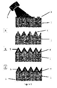
[Figure 1] a schematic of a process for manufacturing an optical element,
which is transparent at a wavelength of use or at a range of wavelengths, and
which
has a super-hydrophobic nanostructured surface that has an anti-reflection
property,
according to one embodiment of the invention.
5 [Figure
2] an XRD spectrum (XRD being the acronym of X-ray diffraction) of
an unstructured A103 layer.
[Figure 3] three SEM images (SEM being the acronym of scanning electron
microscope) of an optical element at various stages of the manufacturing
process of
figure 1.
[Figure 4] two measurements of hardness by nano-indentation of different
materials used in the manufacturing process of figure 1.
DETAILED DESCRIPTION
In the figures, elements that are identical have been designated with the same
references.
By array of pads, what is meant is the spatial arrangement or pattern of the
pads on the nanostructured surface. This pattern is not necessarily periodic.
By "periodic" array of pads, what is meant is pads which recur with a set
pitch
at +10%.
In the case where the array is not periodic, by "pitch" of the array of pads
what
is meant is the minimum distance between the center of any pad of the array
and the
center of its nearest neighbor.
By "nanoscale" dimension of an object, what is meant is a maximum
dimension strictly less than 7.5 pim.
By "vertical", what is meant is a direction perpendicular to the surface.
By "aspect ratio" of an object, what is meant is the ratio between its width
and
its height. By "width", what is meant is the largest dimension in the plane
tangent to
the surface, and by height what is meant is the largest dimension
perpendicular to
the tangent to the surface.
Date Recue/Date Received 2021-09-07
CA 03132787 2021-09-07
6
By "transparent", what is meant here is a transmission greater than 50%,
preferably
75% and even more preferably 95% at one wavelength or in an illumination
wavelength range.
Date Recue/Date Received 2021-09-07
CA 03132787 2021-09-07
7
In order to overcome the problem of the fragility of the nanostructures giving
SH and AR properties to the surface of optical components, the invention
proposes
to cover these nanostructures with a thin conformal layer having a high
hardness. It
is known practice to protect nanostructured optical components by covering
them
with "hard" materials, such as DLC (for diamond-like carbon) for example,
deposited
by CVD or PVD techniques. DLC is deposited more on planar surfaces. DLC alone
exhibits hydrophobic properties. DLC is a material of high hardness (¨ 25 GPa)
and
which also has a hydrophobic character that is modulable via the deposition
conditions. However, it is difficult with deposition by PECVD to obtain a
conformal
profile on nanostructured surfaces having a high aspect ratio such as that
used to
achieve SH and AR properties. However, keeping the shape of the nanostructures
is
essential to meeting optical specifications. The conformity and small
thickness of the
layer covering the nanostructures is therefore essential. It will be recalled
that the
hardness of a material is defined by the resistance that the surface of said
material
shows to the penetration of a harder body.
Figure 1 shows a schematic of the process for manufacturing an optical
element, which is transparent at at least one wavelength of use A and which
has a
super-hydrophobic nanostructured surface that has an anti-reflection property,
according to one embodiment of the invention. In the embodiment of figure 1,
an
optical component (1) is made of germanium and the wavelength of use is
comprised
between 8 and 12 pm. By way of reference, a layer of germanium of 5 mm
thickness
has a transmission of about 50%, corresponding to a transmission of about 70%
per
face for a normal incidence between 8 and 12 pm. This is a material
particularly used
to produce optics in the domain of the thermal infrared. The optical component
1 may
be a window, a lens, a porthole or any other optical element that is
transparent at the
wavelength or in the range of wavelengths of use. The surface to be
nanostructured
of the optical component (1) need not be planar, but may be convex or concave
for
example. The manufacturing process may be broken down into a plurality of
steps.
In step A, a metal film or mask (2) is defined by nanoprinting on the optical
component (1). In another embodiment, the mask is a hard mask obtained by
lithography (optical lithography, block-copolymer lithography or colloidal
lithography).
The metal film or hard film then serves as a mask in the step of etching the
germanium via plasma, ionic or chemical etches or combinations of these
Date Recue/Date Received 2021-09-07
CA 03132787 2021-09-07
8
techniques. In one embodiment, this etching is carried out using an ICP plasma
source (3) (ICP being the acronym of inductively coupled plasma) because this
type
of source allows nanostructures with aspect ratios of up to 1/15 or less,
which are not
achievable with purely chemical etches, to be etched. Specifically, such a
source
allows plasmas of very high density to be generated, allowing very vertical
sidewalls
to be etched. The etching process is carried out by deep reactive ion etching
(DRI
etching) using an ICP source.
Once the etching step A has finished, the mask is removed. The germanium
optical element (1) then has a nanostructured surface (4). The physical
parameters
of the nanostructures are detailed in the description of figure 3. Here it
will merely be
mentioned that, in the embodiment of figure 1, the nanostructures are cones of
height
h, having an aspect ratio generally less than 1/2 and which are arranged in a
periodic
array of pitch p such that p < h.
These physical parameters are chosen so that the nanostructured surface (4)
gives,
to the optical element (1), AR properties, at the wavelength of use il and at
the
angles of incidence of use, and SH properties. The AR effect is due to the
gradual
variation in effective refractive index caused by the nanostructured surface,
which
acts as a pseudo-layer the effective refractive index of which varies between
the
index of air and the refractive index of the material from which the optical
element (1)
is made. Concretely, the height is computed parametrically to maximize the
transmission of the surface depending on the range of wavelengths and of
angles of
incidence of use.
As mentioned above, and depending on the materials used, these
nanostructures may be fragile and highly likely to degrade under difficult
environmental conditions. To overcome this drawback, step B consists in
depositing
a top layer of a material of a hardness greater than the hardness of the
material from
which the nanostructured surface (4) is composed, so as to cover without
discontinuity and conformally said nanostructured surface. Preferably, the top
layer
has a hardness greater by at least 1.3 units on the Mohs scale than the
hardness of
the material from which the nanostructured surface is composed. The thickness
of
the conformal top layer is small, so as to retain the AR and SH properties of
the
optical element. Specifically, too large a thickness (or a non-conformal
layer) would
Date Recue/Date Received 2021-09-07
CA 03132787 2021-09-07
9
effectively protect the nanostructures but would decrease their aspect ratio
and
therefore would negatively impact the SH and AR effect. In the embodiment of
figure
1, the conformal top layer (5) is made of alumina and is deposited by atomic
layer
deposition (ALD). This alumina layer is amorphous and has a thickness less
than
h/5 and greater than h/1000. Alumina (¨ 16 GPa) has a hardness twice as high
as
germanium (¨ 8 GPa) and thus allows the nanostructured surface (4) to be
protected
and the mechanical resistance of the optical element to be increased by
increasing
its hardness and its tenacity. In addition, the conformal top layer acts as an
anti-
corrosion layer allowing the germanium to withstand maritime environments.
In order to increase the hardness of the alumina from which the conformal top
layer is composed, the manufacturing process of figure 1 comprises a last step
C of
applying a thermal anneal to the optical element. In the embodiment of figure
1, the
anneal is carried out at a temperature of 900 C, promoting crystallization of
the
alumina and the appearance of a rhombohedral phase belonging to the sapphire
phase of alumina (6). Step C allows the final germanium optical element (10)
to be
obtained, this element being transparent between 8 and 12 pm and having an SH
nanostructured surface that has an AR property, these properties being made
durable by the deposition of the conformal top layer. The hardness of the
sapphire
phase of alumina is (¨ 25 GPa), this enabling greater protection of the
nanostructured layer (4). In another embodiment, the step of applying a
thermal
anneal to the alumina is carried out at a temperature comprised between 500 C
and
1200 C via standard or rapid thermal annealing (RTA) or even laser annealing.
In
another embodiment, the material from which the top layer is made is DLC or
ZrO2,
for example.
In order to confirm the appearance of the sapphire phase of alumina, an XRD
spectrum (XRD being the acronym of X-ray diffraction) of an alumina layer
deposited
on a silicon substrate is carried out. Figure 2 shows the result of this
measurement.
The x-axis represents the angles of the diffraction peaks associated with the
various
crystal structures and the y-axis corresponds to the logarithm of the
intensity of the
various diffraction peaks. The bottom curve corresponds to the analysis of the
silicon
substrate alone. The curve comprised between the two curves corresponds to the
spectrum of the amorphous alumina layer (5) of 200 nm thickness deposited by
ALD
on the silicon substrate. Lastly, the top curve corresponds to the
spectroscopy of the
Date Recue/Date Received 2021-09-07
CA 03132787 2021-09-07
alumina layer (6) after thermal annealing at a temperature of 900 C. The
appearance, on the top curve, of the diffraction peak corresponding to the
sapphire
phase of the alumina layer (6) obtained after thermal annealing (black
rectangle) at
900 C of the alumina layer (5) deposited by ALD may very clearly be seen. This
5 diffraction peak is obviously not observable during the analysis of the
alumina layer
(5) before thermal annealing.
Figure 3 groups together three SEM images (SEM being the acronym of
scanning electron microscope) of the nanostructured germanium surface of the
optical element obtained using the manufacturing process of figure 1 at
various
10 stages of the manufacturing process.
Image A is an SEM image of the nanostructured germanium surface after step
A of a manufacturing process similar to that of figure 1. The nanostructures
produced
by plasma etching using an ICP source are cones of height h = 3.2 ym and of
aspect
ratio R = Llh = 1/6, L being the width of the cones. The cones are distributed
in a
regular array with a pitch of periodicity p = 1.6 m. These cone parameters
allow SH
and AR properties to be given to the nanostructured surface. Generally, an
aspect
ratio of less than 1/2 and preferably less than 1/3 is sufficient to obtain SH
properties.
In another embodiment, the nanostructures have a height h such that h <A.,
with an
aspect ratio R <1110 and an array pitch p such that p < h . In one alternative
embodiment, the nanostructures patterned on the surface are not arranged
periodically but with a sufficiently small array pitch (or a sufficiently
dense array) to
obtain an SH and AR effect. In this case, the minimum distance between any
cone of
the array and its nearest neighbor is comprised between h13 and 2h/3. The
nanostructures may be pads, cylinders or cones or truncated cones. By
cylinder,
what is meant here is any solid the lateral surface of which is a ruled
surface the
generatrices of which are parallel, this including parallelograms for example.
By
cone, what is meant is any solid the lateral surface of which is a ruled
surface the
generatrices of which pass through a given point (the vertex), this including
pyramids
.. for example.
Image B1 of figure 3 shows the nanostructured surface (4) of the optical
element, as obtained after step B of the manufacturing process of figure 1.
Here, the
Date Recue/Date Received 2021-09-07
CA 03132787 2021-09-07
11
nanostructured surface (4) is covered without discontinuity by the conformal
top layer
of alumina, which is 200 nm thick, using ALD. In another embodiment the
thickness
e of the top layer is less than h/5, preferably less than h/10 and more
preferably
less than h/20. Since alumina is harder than germanium (16 GPa vs 8 GPa), this
conformal layer allows the nanostructures to be protected while keeping the SH
and
AR properties of the surface. In another embodiment, the deposit of the
conformal
top layer is made of a material at least two times and preferably three times
harder
than that from which the nanostructured surface of the optical element (1) is
composed.
The image B2 corresponds to a cross-sectional view of image B1 of figure 3
produced using a focused ion beam. This cross section allows the conformity of
the
alumina layer (5) deposited by ALD to be observed. It will be recalled that
the
nanostructures are 3.2 m high and that the alumina layer is 200 nm thick.
In order to study more precisely the effect of the conformal top layer on the
hardness of the surface of the optical element (10), nano-indentation tests
were
carried out using an atomic force microscope (AFM). The principle consists in
indenting, with a defined force, the material to be studied using a diamond
tip (with a
hardness comprised between 70 and 150 GPa), then in measuring the residual
imprint with a tip having a smaller radius of curvature. Materials may then be
classified by hardness, depending on the depth of the residual indentation:
the harder
a material, the shallower the indentation depth. Tests were carried out on the
one
hand on a silicon surface and on a silicon surface covered with amorphous
alumina
with a force of 350 /IN, and on the other hand on a silicon surface covered
with
amorphous alumina and on a silicon surface covered with alumina annealed at
900 C with a force of 500 N . The results of the nano-indentation tests are
presented
in figure 4. The top graph shows the comparative measurement by AFM of the
indentation of silicon and of amorphous alumina (without anneal) deposited on
silicon
by ALD. The depth of the residual indentation with a force of 350 N is ¨ 12
nm on
the germanium and ¨ 5 nm on the alumina. The depth of the residual indentation
with
a force of 500 N is ¨ 25 nm on the alumina without anneal and ¨ 15 nm on the
alumina after annealing at 900 C.
Date Recue/Date Received 2021-09-07
CA 03132787 2021-09-07
12
These measurements therefore make it possible to confirm that the hardness
of the annealed alumina is greater than that of amorphous alumina, which is
greater
than that of silicon. Thus, the conformal top layer (6) of annealed alumina
enables
additional protection of the nanostructures, operation of the optical element
(10)
under severe environmental conditions and longer retention of the SH and AR
properties.
In another embodiment the wavelengths of use are comprised in a wavelength
range comprised between 100 nm and 25 pm . In another embodiment, the
nanostructured surface (4) (and the optical component (1)) of the optical
element (10)
is made of oxide glass, borosilicate, silicon, silica, halide, chalcogenide or
ZnS, ZnSe
or even polycarbonate. In another embodiment, the nanostructured surface is
made
of a material that is transparent in the visible spectrum (for example of BK-7
glass),
the wavelength of use belonging to the visible spectrum.
In another embodiment the conformal top layer (5) may be made of any type of
material which is transparent at the wavelength of use, which may be deposited
in a
conformal layer by ALD and which has a hardness greater than that of the
material of
the nanostructured surface (4). Preferably, the top layer has a hardness
greater by at
least 1.3 units on the Mohs scale than the hardness of the material of the
nanostructured surface (4).
Date Recue/Date Received 2021-09-07