Note: Descriptions are shown in the official language in which they were submitted.
METHOD OF PROCESSING WAFER
BACKGROUND OF THE INVENTION
Field of the Invention
The present invention relates to a method of
processing a wafer.
Description of the Related Art
Electronic devices represented by mobile phones and
personal computers include as indispensable components
device chips having devices such as electronic circuits.
Device chips are fabricated by demarcating the face side
of a wafer made of a semiconductor such as silicon into a
plurality of areas along projected dicing lines known as
streets, forming devices in the respective areas, and
then dividing the wafer along the projected dicing lines.
The devices described above are generally formed by
stacking metal films, insulating films, etc. on the wafer
in a thickness direction thereof and processing the
stacked films according to predetermined patterns
corresponding to the devices. The metal films, the
insulating films, etc. are processed, for example, by an
etching process in which an etchant such as a highly
reactive gas, a chemical solution, or the like is applied
to a target film through a mask in the form of a resist
1
Date Recue/Date Received 2021-10-12
film produced by coating the target film with a liquid
material by a spin coating process (see, for example,
Japanese Patent Laid-Open No. Hei 8-44064).
SUMMARY OF THE INVENTION
When the resist film is formed on the wafer by the
spin coating process, the resist film tends to swell in a
thicker shape or a granular shape on an outer
circumferential edge portion of the wafer, and hence is
highly likely to decrease in planarity. In the thicker
swelling portion of the resist film, the solvent is not
sufficiently removed by a subsequent prebaking process.
Therefore, in a case where a contact-type exposure
process is carried out to expose the resist film to light
through a photomask held in contact with the resist film,
the material of the resist film is liable to stick to the
photomask.
In addition, a gas may be also trapped in the
thicker swelling portion of the resist film. In a case
where the gas is trapped in the thicker swelling portion
of the resist film, the trapped gas tends to expand in a
subsequent heating process, i.e., a heating process that
is carried out to paste the wafer with the resist film
formed thereon to another wafer, possibly bursting the
2
Date Recue/Date Received 2021-10-12
thicker swelling portion of the resist film and
contaminating the environment with resist film fragments.
It is therefore an object of the present invention
to provide a method of processing a wafer in a manner to
make it less likely to have a resist film swell on an
outer circumferential edge portion of the wafer.
In accordance with an aspect of the present
invention, there is provided a method of processing a
wafer having a first surface and a second surface
opposite the first surface, including the steps of:
holding the second surface of the wafer such that the
first surface thereof is exposed; after holding the
second surface of the wafer, processing an exposed first
surface side of an outer circumferential edge portion of
the wafer with a processing tool including a grinding
stone made of abrasive grains bound together by a bonding
material, thereby forming on the outer circumferential
edge portion a slanted surface that is inclined to the
first surface so as to be progressively closer to the
second surface in a direction from a central area of the
wafer toward an outer circumferential edge thereof; and
after forming the slanted surface, coating the first
surface of the wafer with a liquid material according to
a spin coating process, thereby forming a resist film on
3
Date Recue/Date Received 2021-10-12
the first surface of the wafer.
Alternatively, in accordance with an aspect of the
present invention, the processing tool includes a
frustoconical cutting blade including a first side
surface having a circular outer circumferential edge, a
second side surface having a circular outer
circumferential edge that is larger in diameter than the
first side surface and positioned opposite the first side
surface, and an outer circumferential surface formed of
the grinding stone and connecting the outer
circumferential edge of the first side surface and the
outer circumferential edge of the second side surface to
each other, the outer circumferential surface being
inclined to the first side surface and the second side
surface, and the step of forming the slanted surface
includes the step of causing the cutting blade to cut
into the outer circumferential edge portion of the wafer
such that the second side surface of the cutting blade is
positioned closer to the outer circumferential edge of
the wafer.
Alternatively, in accordance with an aspect of the
present invention, the processing tool includes a disk-
shaped cutting blade including a first side surface
having a circular outer circumferential edge, a second
4
Date Recue/Date Received 2021-10-12
side surface having a circular outer circumferential edge
and positioned opposite the first side surface, and an
outer circumferential surface formed of the grinding
stone and connecting the outer circumferential edge of
the first side surface and the outer circumferential edge
of the second side surface to each other, and the step of
forming the slanted surface includes the step of causing
the cutting blade to cut into the outer circumferential
edge portion of the wafer while the cutting blade is
being rotated by a rotational shaft inclined to the first
surface of the wafer.
Further alternatively, in accordance an aspect of
the present invention, the processing tool includes a
grinding wheel having the grinding stone.
In the method of processing a wafer according to an
aspect of the present invention, since the slanted
surface that is inclined to the first surface so as to be
progressively closer to the second surface in the
direction from the central area of the wafer toward an
outer circumferential edge thereof is formed on the first
surface side of the outer circumferential edge portion of
the wafer, when a liquid material that is to turn into a
resist film is applied to the first surface of the wafer
by a spin coating process, it is easy for the liquid
Date Recue/Date Received 2021-10-12
89073391
material to flow down the slanted surface and drain off from the
wafer 11 to the outside thereof, upon flowing from the central
area of the wafer toward the outer circumferential edge thereof.
In other words, as the liquid material is less likely to
accumulate on the outer circumferential edge portion of the
wafer, the possibility that the resist film formed from the
applied liquid material will swell on the outer circumferential
edge portion of the wafer is reduced.
According to one aspect of the present invention, there
is provided a method of processing a wafer having a first
surface and a second surface opposite the first surface,
comprising the steps of: holding the second surface of the wafer
such that the first surface thereof is exposed; positioning a
processing tool including a rotational axis relative to the
first surface of the wafer so that the rotational axis is at an
angle relative to the first surface of the wafer, wherein the
angle is between 0 and 90 , and wherein the processing tool
includes a grinding stone made of abrasive grains bound together
by a bonding material; after holding the second surface of the
wafer, processing an exposed first surface side of an outer
circumferential edge portion of the wafer without processing the
second surface of the wafer, with the processing tool, thereby
forming on the outer circumferential edge portion a slanted
surface that is inclined to the first surface so as to be
progressively closer to the second surface in a direction from a
central area of the wafer toward an outer circumferential edge
thereof; and after forming the slanted surface, coating the
first surface of the wafer with a liquid material according to a
spin coating process, thereby forming a resist film on the first
surface of the wafer.
According to another aspect of the present invention,
there is provided a method of processing a wafer having a first
surface and a second surface opposite the first surface,
comprising the steps of: holding the second surface of the
6
Date Rectie/Date Received 2023-03-20
89073391
wafer such that the first surface thereof is exposed; after
holding the second surface of the wafer, processing an exposed
first surface side of an outer circumferential edge portion of
the wafer without processing the second surface of the wafer,
with a processing tool, thereby forming on the outer
circumferential edge portion a slanted surface that is inclined
to the first surface so as to be progressively closer to the
second surface in a direction from a central area of the wafer
toward an outer circumferential edge thereof, wherein the
processing tool includes a frustoconical cutting blade including
a first side surface having a circular outer circumferential
edge, a second side surface having a circular outer
circumferential edge that is larger in diameter than the first
side surface and positioned opposite the first side surface, and
an outer circumferential surface formed by a grinding stone and
connecting the outer circumferential edge of the first side
surface and the outer circumferential edge of the second side
surface to each other, the outer circumferential surface being
inclined to the first side surface and the second side surface,
and wherein forming the slanted surface includes the step of
causing the cutting blade to cut into the outer circumferential
edge portion of the wafer such that the second side surface of
the cutting blade is positioned closer to the outer
circumferential edge of the wafer, after forming the slanted
surface, coating the first surface of the wafer with a liquid
material according to a spin coating process, thereby forming a
resist film on the first surface of the wafer.
The above and other objects, features and advantages of the
present invention and the manner of realizing them will become
more apparent, and the invention itself will best be understood
from a study of the following description and the attached
drawings showing preferred embodiments of the invention.
6a
Date Rectie/Date Received 2023-03-20
89073391
BRIEF DESCRIPTION OF THE DRAWINGS
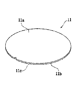
FIG. 1 is a perspective view of a wafer;
FIG. 2 is a cross-sectional view illustrating a
manner in which the wafer is held in place in a method of
processing a wafer according to a first embodiment of the
present invention;
FIG. 3 is a cross-sectional view illustrating a
6b
Date Rectie/Date Received 2023-03-20
manner in which a slanted surface is formed on the wafer
in the method of processing a wafer according to the
first embodiment;
FIG. 4 is an enlarged fragmentary cross-sectional
view of the wafer with the slanted surface formed
thereon;
FIG. 5 is a cross-sectional view illustrating a
manner in which a resist film is formed on the wafer in
the method of processing a wafer according to the first
embodiment;
FIG. 6 is an enlarged fragmentary cross-sectional
view of the wafer with the slanted surface and the resist
film on the wafer;
FIG. 7 is an enlarged fragmentary cross-sectional
view of a wafer with no slanted surface and with a resist
film on the wafer;
FIG. 8 is a cross-sectional view illustrating a
manner in which a slanted surface is formed on the wafer
in a method of processing a wafer according to a second
embodiment of the present invention;
FIG. 9 is a cross-sectional view illustrating a
manner in which a slanted surface is formed on the wafer
in a method of processing a wafer according to a third
embodiment of the present invention; and
7
Date Recue/Date Received 2021-10-12
FIG. 10 is a cross-sectional view illustrating a
manner in which a slanted surface is formed on the wafer
in a method of processing a wafer according to a fourth
embodiment of the present invention.
DETAILED DESCRIPTION OF THE PREFERRED EMBODIMENTS
Preferred embodiments of the present invention will
be described in detail below with reference to the
accompanying drawings.
(First Embodiment)
FIG. 1 illustrates in perspective a wafer 11 to be
processed by a method of processing a wafer according to
a first embodiment of the present invention. As
illustrated in FIG. 1, the wafer 11 is made of a
semiconductor such as silicon and is of a disk shape
having a first surface ha and a second surface lib
opposite the first surface 11a, i.e., on the back side of
the wafer 11. Each of the first surface ha and the
second surface llb is of a generally flat circular shape.
In addition, the first surface lla and the second surface
lib are joined to each other by an outer circumferential
edge surface 11c curved by beveling.
The wafer 11 is free of devices such as electronic
circuits. However, the method of processing a wafer
8
Date Recue/Date Received 2021-10-12
according to the present embodiment is also able to
process a wafer with devices formed thereon. The wafer 11
is not limited to any materials, structures, sizes, etc.
For example, wafers made of other semiconductors,
ceramics, resins, metals, or the like can be processed by
the method of processing a wafer according to the present
embodiment. Furthermore, the wafer 11 may be pasted to
another wafer, a substrate, or the like in a subsequent
step.
In the method of processing a wafer according to
the present embodiment, the second surface lib of the
wafer 11 is held in place such that the first surface ha
thereof is exposed (holding step). FIG. 2 illustrates in
cross section a manner in which the wafer 11 is held in
place. In FIG. 2, some components are represented by
symbols and a functional block.
The wafer 11 is held in place using a processing
apparatus 2 illustrated in FIG. 2, for example. The
processing apparatus 2 includes a chuck table, i.e.,
holding table, 4 configured to be able to hold the wafer
11 thereon. The chuck table 4 includes a cylindrical
frame 6 made of a metal material such as stainless steel,
for example, and having a recess defined in an upper
surface thereof. The frame 6 has a fluid channel 6a
9
Date Recue/Date Received 2021-10-12
defined therein for transmitting a negative pressure to
be used for attracting the wafer 11 under suction on the
chuck table 4.
The chuck table 4 also includes a porous plate 8
securely placed in the recess of the frame 6. The porous
plate 8 is made of ceramics and hence is rendered porous
thereby. The porous plate 8 has an upper surface, i.e.,
holding surface, 8a for holding the wafer 11 thereon. A
suction source 12 such as a vacuum pump is connected
through a valve 10 to the fluid channel 6a in the frame
6. When the valve 10 is opened while the suction source
12 is in operation, a vacuum pressure generated by the
suction source 12 is transmitted through the valve 10 and
the fluid channel 6a and acts on the upper surface 8a of
the porous plate 8.
A rotary actuator, not depicted, such as an
electric motor is coupled to the frame 6 of the chuck
table 4. When the rotary actuator is energized, it
generates and transmits rotational power to the frame 6,
rotating the chuck table 4 about a central axis generally
perpendicular to the upper surface 8a of the porous plate
8. In addition, the frame 6 of the chuck table 4 is
supported on a table moving mechanism, not depicted. The
table moving mechanism moves the frame 6 in a first
Date Recue/Date Received 2021-10-12
direction, i.e., a first horizontal direction, generally
parallel to the upper surface Ba of the porous plate 8.
For holding the wafer 11 on the chuck table 4, the
second surface llb of the wafer 11 is brought into
contact with the upper surface 8a of the porous plate 8,
for example, as illustrated in FIG. 2. Then, the valve 10
is opened while the suction source 12 is in operation,
allowing the vacuum pressure from the suction source 12
to act on the upper surface 8a of the porous plate 8.
Accordingly, the second surface llb of the wafer 11 is
attracted under suction to the upper surface 8a of the
porous plate 8. In other words, the second surface llb of
the wafer 11 is held under suction on the chuck table 4
with the first surface ha exposed upwardly.
According to the present embodiment, the second
surface llb of the wafer 11 is held in direct contact
with the upper surface 8a of the porous plate 8. However,
a protective member such as a tape may be affixed to the
second surface llb of the wafer 11 in advance. With the
protective member affixed to the second surface 11b, the
second surface llb of the wafer 11 is held on the chuck
table 4 with the protective member interposed
therebetween and can be hence protected against damage
due to contact with the porous plate 8 or the like.
11
Date Recue/Date Received 2021-10-12
After the second surface 11b of the wafer 11 has
been held on the chuck table 4, an outer circumferential
edge portion of the first surface 11a of the wafer 11 is
processed to form a slanted surface thereon (processing
step). FIG. 3 illustrates in cross section a manner in
which a slanted surface 11d is formed on the wafer 11. In
FIG. 3, some components are represented by symbols and a
functional block.
The slanted surface 11d is formed also using the
processing apparatus 2. As illustrated in FIG. 3, a
cutting unit, i.e., a processing unit, 14 is disposed
above the chuck table 4. The cutting unit 14 includes a
spindle 16 that has a central axis generally parallel to
the upper surface 8a of the porous plate 8 and generally
perpendicular to the first direction. A cutting blade,
i.e., a processing tool, 18 including a grinding stone
made of abrasive grains bound together by a bonding
material is mounted on one end of the spindle 16.
The other end of the spindle 16 is coupled to a
rotary actuator, not depicted, such as an electric motor.
When the rotary actuator is energized, it generates and
transmits rotational power to the spindle 16, rotating
the cutting blade 18 mounted on the other end of the
spindle 16 about the central axis thereof. The cutting
12
Date Recue/Date Received 2021-10-12
unit 14 is supported on a cutting unit moving mechanism,
not depicted. The cutting unit moving mechanism moves the
cutting unit 14 in a second direction, i.e., a second
horizontal direction, generally parallel to the upper
surface 8a of the porous plate 8 and generally
perpendicular to the first direction, and in a third
direction, i.e., a vertical direction, generally
perpendicular to the first direction and the second
direction.
The cutting blade 18 is of a frustoconical shape
including a first side surface 18a having a circular
outer circumferential edge and a second side surface 18b
having a circular outer circumferential edge that is
larger in diameter than the first side surface 18a and
positioned opposite the first side surface 18a, i.e., on
the back side of the cutting blade 18, for example. The
outer circumferential edge of the first side surface 18a
and the outer circumferential edge of the second side
surface 18b are connected to each other by an outer
circumferential surface 18c inclined to both the first
side surface 18a and the second side surface 18b. In
addition, at least the outer circumferential surface 18c
is formed of a grinding stone made of abrasive grains
such as diamond or the like bound together by a bonding
13
Date Recue/Date Received 2021-10-12
material such as a resin.
The cutting blade 18 is mounted on the one end of
the spindle 16 such that the first side surface 18a and
the second side surface 18b lie generally perpendicular
to the axis of the spindle 16. In other words, the first
side surface 18a and the second side surface 18b lie
generally perpendicular to the second direction.
The width or thickness of the cutting blade 18,
i.e., the distance between the first side surface 18a and
the second side surface 18b, is optionally set to a value
matching the desired width of the slanted surface 11d to
be formed. For example, the slanted surface lid that is
of a sufficient width can easily be formed on the wafer
11 by using the cutting blade 18 whose width is in a
range from 0.5 mm to 3.0 mm, typically of 1 mm.
For forming the slanted surface lid on the wafer
11, as illustrated in FIG. 3, the cutting blade 18 as it
is rotated by the spindle 16 about the axis thereof is
caused to cut into the outer circumferential edge portion
of the wafer 11 that includes the boundary between the
first surface 11a and the outer circumferential edge
surface 11c of the wafer 11. At this time, the cutting
blade 18 is caused to cut into the outer circumferential
edge portion of the wafer 11 such that the first side
14
Date Recue/Date Received 2021-10-12
surface 18a of the cutting blade 18 is positioned closer
to the center of the wafer 11 and the second side surface
18b of the cutting blade 18 is positioned closer to the
outer circumferential edge of the wafer 11. Then, the
chuck table 4 is rotated to make one revolution about its
own central axis.
The height of the cutting unit 14 at the time that
the cutting blade 18 cuts into the wafer 11 is adjusted
in such a range that only the outer circumferential
surface 18c of the cutting blade 18 contacts the wafer
11. Specifically, for example, the height of the cutting
unit 14 is adjusted such that the height of the lower end
of the first side surface 18a of the cutting blade 18 is
equal to or larger than the height of the first surface
ha of the wafer 11 and the height of the lower end of
the second side surface 18b of the cutting blade 18 is
smaller than the height of the first surface ha.
The cutting blade 18 is thus allowed to cut into
the first surface ha side of the outer circumferential
edge portion of the wafer 11, forming the slanted surface
lid that is joined to the first surface 11a without
abrupt height differences. The slanted surface 11d thus
formed is inclined to the first surface 11a so as to be
progressively closer to the second surface 11b of the
Date Recue/Date Received 2021-10-12
wafer 11 in a direction from a central area of the wafer
11 toward an outer circumferential edge thereof.
Specifically, the height of the slanted surface lid
is smaller on the outer circumferential edge surface llc
side, i.e., on an outer side of the wafer 11, than on the
first surface ha side, i.e., on an inner side of the
wafer 11. The thickness of the wafer 11 in the outer
circumferential edge portion thereof where the slanted
surface lid is formed is smaller on the outer
circumferential edge surface 11c side than on the first
surface ha side.
FIG. 4 illustrates in enlarged fragmentary cross
section the wafer 11 with the slanted surface lid formed
thereon. As illustrated in FIG. 4, the angle e formed
between the first surface ha and the slanted surface lid
should preferably be adjusted in a range from 100 to 25 ,
for example. The angle 9 thus adjusted is effective to
keep sufficiently low the possibility that a resist film
to be formed on the first surface ha of the wafer 11
will swell on the outer circumferential edge portion of
the wafer 11. Meanwhile, the width W of the slanted
surface 11d, i.e., the length of the slanted surface lid
along radial directions of the wafer 11, is adjusted in a
range from 0.5 mm to 3.0 mm. However, there is no
16
Date Recue/Date Received 2021-10-12
particular limitation on the width W.
After the slanted surface lid has been formed on
the wafer 11, a liquid material is applied to the first
surface ha of the wafer 11 by a spin coating process,
thereby forming a resist film on the first surface 11a of
the wafer 11 (resist film forming step). FIG. 5
illustrates in cross section a manner in which a resist
film is formed on the wafer 11. The resist film is formed
using a spin coater 22 illustrated in FIG. 5, for
example.
As illustrated in FIG. 5, the spin coater 22
includes a hollow cylindrical housing 24 that houses the
wafer 11 and the like therein. The housing 24 has therein
a space 24a as a processing chamber in which a resist
film will be formed on the wafer 11. A disk-shaped
spinner table 26 that is smaller in diameter than the
wafer 11 is disposed centrally in the space 24a. The
spinner table 26 has an upper surface, i.e., a holding
surface, 26a for holding the wafer 11 thereon.
A suction source, not depicted, such as a vacuum
pump is connected to the upper surface 26a of the spinner
table 26 through a fluid channel, not depicted, defined
in the spinner table 26 and a valve, not depicted. When
the valve is opened while the suction source is in
17
Date Recue/Date Received 2021-10-12
operation, a vacuum pressure generated by the suction
source can be transmitted through the valve and the fluid
channel and act on the upper surface 26a of the spinner
table 26. A rotary actuator 30 such as an electric motor
is coupled to a lower portion of the spinner table 26
through a spindle 28. When the rotary actuator 30 is
energized, it generates and transmits rotational power
through the spindle 28 to the spinner table 26, rotating
the spinner table 26 about its own central axis.
The spin coater 22 also includes a nozzle 32
disposed above the spinner table 26, for dropping a
liquid material 13 from its distal end onto the first
surface ha of the wafer 11. The nozzle 32 has a proximal
end coupled to a rotary actuator 34 such as an electric
motor. When the rotary actuator 34 is energized, it
generates and transmits rotational power to the nozzle
32, moving the distal end of the nozzle 32 to follow an
arcuate path over the spinner table 26. When the liquid
material 13 is to be dropped onto the wafer 11, the
distal end of the nozzle 32 is moved from a retracted
region at an end of the space 24a to a dropping region
directly above the spinner table 26.
For forming a resist film on the first surface 11a
of the wafer 11, the second surface 11b of the wafer 11
18
Date Recue/Date Received 2021-10-12
is brought into contact with the upper surface 26a of the
spinner table 26, as illustrated in FIG. 5, for example.
Then, the valve is opened while the suction source is in
operation, applying the vacuum pressure to the upper
surface 26a of the spinner table 26. The second surface
11b of the wafer 11 is now attracted under suction to the
upper surface 26a of the spinner table 26. In other
words, the second surface lib of the wafer 11 is held
under suction on the spinner table 26 with the first
surface 11a exposed upwardly.
Next, the distal end of the nozzle 32 is moved to
the dropping region directly above the spinner table 26.
The nozzle 32 then drops the liquid material 13 from the
distal end thereof onto the first surface 11a of the
wafer 11 held on the spinner table 26. More specifically,
the distal end of the nozzle 32 is positioned above a
central area of the wafer 11 and drops the liquid
material 13 onto the upper surface ha of the central
area of the wafer 11.
Then, the spinner table 26 is rotated about its own
central axis by the rotary actuator 30. The spinner table
26 is rotated at a rotational speed in a range from 1000
rpm to 3000 rpm, for example. The spinner table 26 is
rotated for a period of time in a range from 10 seconds
19
Date Recue/Date Received 2021-10-12
to 60 seconds, for example. However, there is no
particular limitation on the conditions under which to
rotate the spinner table 26, for example.
For example, the spinner table 26 may be rotated at
a combination of different rotational speeds, e.g., a
high rotational speed in a range from 1000 rpm to 3000
rpm and a low rotational speed in a range from 10 rpm to
300 rpm. The rotation of the spinner table 26 causes the
liquid material 13 that has been dropped on the wafer 11
to be spread all over the first surface ha thereof. In
other words, the first surface ha of the wafer 11 is
coated in its entirety with the liquid material 13.
According to the present embodiment, an epoxy resin
such as SU-8 or the like that is suitable for forming a
resist film is used as the liquid material 13. However,
there is no particular limitation on the liquid material
13 as well. The liquid material 13 may be changed
depending on properties required for the resist film to
be formed, for example.
After the liquid material 13 has been spread all
over the first surface 11a of the wafer 11, the applied
liquid material 13 is dried to evaporate the solvent and
water contained in the liquid material 13. For example,
the wafer 11 with the liquid material 13 spread thereon
Date Recue/Date Received 2021-10-12
is placed on a hot plate that has been heated to a
temperature in a range from 80 C to 120 C and left on the
hot plate for approximately 60 seconds, drying the liquid
material 13 together with the wafer 11. When the liquid
material 13 is dried, it turns into a resist film 15 (see
FIG. 6) covering the first surface 11a in its entirety.
However, there is also no particular limitation on the
conditions under which to dry the liquid material 13.
For example, after the nozzle 32 has stopped
supplying the liquid material 13, the spinner table 26
may be continuously rotated to dry the liquid material 13
applied to the first surface 11a of the wafer 11.
Alternatively, an oven, i.e., a drying furnace, a heater,
a lamp, or the like may be used in place of the hot plate
to heat and dry the liquid material 13. For example, the
wafer 11 coated with the liquid material 13 may be
introduced into an oven heated to a temperature in a
range from 80 C to 120 C to dry the liquid material 13.
The oven may heat the wafer 11 for a period of time in a
range from approximately 10 minutes to approximately 20
minutes, in this case.
FIG. 6 illustrates in enlarged fragmentary cross
section the wafer 11 with the slanted surface lid formed
thereon and the resist film 15 formed on the wafer 11. As
21
Date Recue/Date Received 2021-10-12
illustrated in FIG. 6, according to the present
embodiment, since the slanted surface lid is formed on
the first surface 11a side of the outer circumferential
edge portion of the wafer 11, when the liquid material 13
that is to turn into the resist film 15 is applied to the
first surface 11a of the wafer 11 by the spin coating
process, it is easy for the liquid material 13 to flow
down the slanted surface lld and drain off from the wafer
11 to the outside thereof, upon flowing from the central
area of the wafer 11 toward the outer circumferential
edge thereof.
In other words, as the liquid material 13 is less
likely to accumulate on the outer circumferential edge
portion of the wafer 11, the possibility that the resist
film 15 will swell on the outer circumferential edge
portion of the wafer 11 is reduced. FIG. 7 illustrates in
enlarged fragmentary cross section a wafer 21 with no
slanted surface and with a resist film 25 formed on the
wafer 21.
The wafer 21 is similar to the wafer 11 except that
no slanted surface is formed thereon. Specifically, the
wafer 21 is of a disk shape having a first surface 21a
and a second surface 21b opposite the first surface 21a,
i.e., on the back side of the wafer 21. The first surface
22
Date Recue/Date Received 2021-10-12
21a and the second surface 21b are joined to each other
by an outer circumferential edge surface 21c curved by
beveling.
If a resist film 25 is formed on the first surface
21a of the wafer 21 by a spin coating process, as
illustrated in FIG. 7, the resist film 25 is highly
likely to form a thicker swelling portion 25a on the
outer circumferential edge portion of the wafer 21.
Specifically, since no slanted surface is formed on the
wafer 21, the liquid material 13 tends to accumulate on
the outer circumferential edge portion of the wafer 21.
When the spinner table 26 is rotated, the accumulated
liquid material 13 on the outer circumferential edge
portion of the wafer 21 is locally dried by an air
stream, i.e., turbulence, produced on the outer
circumferential edge portion of the wafer 21 by the
rotation of the spinner table 26, resulting in the
thicker swelling portion 25a thereon.
In the method of processing a wafer according to
the present embodiment, as described above, inasmuch as
the slanted surface lld that is inclined to the first
surface lla so as to be progressively closer to the
second surface 11b of the wafer 11 in the direction from
the central area of the wafer 11 toward the outer
23
Date Recue/Date Received 2021-10-12
circumferential edge thereof is formed on the first
surface ha side of the outer circumferential edge
portion of the wafer 11, when the liquid material 13 that
is to turn into the resist film 15 is applied to the
first surface ha of the wafer 11 by the spin coating
process, it is easy for the liquid material 13 to flow
down the slanted surface lid and drain off from the wafer
11 to the outside thereof, upon flowing from the central
area of the wafer 11 toward the outer circumferential
edge thereof.
In other words, as the liquid material 13 is less
likely to accumulate on the outer circumferential edge
portion of the wafer 11, the possibility that the resist
film 15 will swell on the outer circumferential edge
portion of the wafer 11 is reduced even in a situation
where the liquid material 13 applied to the wafer 11 is
liable to be locally dried by an air stream, i.e.,
turbulence, produced around the wafer 11 by the rotation
of the wafer 11.
(Second Embodiment)
A method of processing a wafer according to a
second embodiment of the present invention will be
described in detail below. According to the second
embodiment, a slanted surface lid is formed on a wafer 11
24
Date Recue/Date Received 2021-10-12
in a manner different from the first embodiment described
above. Other details of the method according to the
second embodiment than the processing step of forming the
slanted surface lid on the wafer 11 are the same as those
of the method according to the first embodiment.
Therefore, different details of the method according to
the second embodiment will mainly be described below.
FIG. 8 illustrates in cross section a manner in
which the slanted surface 11d is formed on the wafer 11
in the method according to the present embodiment. In
FIG. 8, some components are represented by symbols and a
functional block.
The method of processing a wafer according to the
present embodiment is carried out using a processing
apparatus 42 illustrated in FIG. 8. Specifically, the
second surface lib of the wafer 11 is held on the chuck
table 4 of the processing apparatus 42 (holding step),
and thereafter, the slanted surface lid is formed on the
wafer 11 by the processing apparatus 42 (processing
step). Some components of the processing apparatus 42 are
identical to those of the processing apparatus 2
described above. Therefore, those components of the
processing apparatus 42 that are identical to those of
the processing apparatus 2 are denoted by identical
Date Recue/Date Received 2021-10-12
reference characters, and their description will be
omitted below.
As illustrated in FIG. 8, a cutting unit, i.e., a
processing unit, 54 is disposed above the chuck table 4.
The cutting unit 54 includes a spindle, or a rotational
shaft, 56 that is capable of changing the angle of its
own central axis with respect to the upper surface 8a of
the porous plate 8, for example. A cutting blade, i.e., a
processing tool, 58 including a grinding stone made of
abrasive grains bound together by a bonding material is
mounted on one end of the spindle 56.
The other end of the spindle 56 is coupled to a
rotary actuator, not depicted, such as an electric motor.
When the rotary actuator is energized, it generates and
transmits rotational power to the spindle 56, rotating
the cutting blade 58 on the spindle 56 about the central
axis thereof. The cutting unit 54 is supported on a
cutting unit moving mechanism, not depicted, for example.
The cutting unit moving mechanism moves the cutting unit
54 in a second direction, i.e., a second horizontal
direction, generally parallel to the upper surface 8a of
the porous plate 8 and generally perpendicular to the
first direction in which the chuck table 4 is movable,
and in a third direction generally perpendicular to the
26
Date Recue/Date Received 2021-10-12
first direction and the second direction.
The cutting blade 58 is of a disk shape including a
first side surface 58a having a circular outer
circumferential edge and a second side surface 58b having
a circular outer circumferential edge that is of the same
diameter as the first side surface 58a and positioned
opposite the first side surface 58a, i.e., on the back
side of the cutting blade 58. The outer circumferential
edge of the first side surface 58a and the outer
circumferential edge of the second side surface 58b are
connected to each other by an outer circumferential
surface 58c. In addition, at least the outer
circumferential surface 58c is formed as a grinding stone
made of abrasive grains such as diamond bound together by
a bonding material such as a resin.
The cutting blade 58 is mounted on the one end of
the spindle 56 such that the first side surface 58a and
the second side surface 58b lie generally perpendicularly
to the central axis of the spindle 56. The width or
thickness of the cutting blade 58, i.e., the distance
between the first side surface 58a and the second side
surface 58b, is optionally set to a value matching the
desired width of the slanted surface lid to be formed.
For example, the slanted surface lid that is of a
27
Date Recue/Date Received 2021-10-12
sufficient width can easily be formed on the wafer 11 by
using the cutting blade 58 whose width is in a range from
0.5 mm to 3.0 mm, typically of 1 mm.
For forming the slanted surface lid on the wafer
11, the spindle 56 as the rotational shaft is inclined
with respect to the upper surface 8a of the porous plate
8, as illustrated in FIG. 8. In other words, the spindle
56 is inclined with respect to the first surface ha and
the second surface lib of the wafer 11. Thereafter, the
cutting blade 58 as it is rotated about the central axis
thereof by the spindle 56 is caused to cut into the outer
circumferential edge portion of the wafer 11 that
includes the boundary between the first surface ha and
the outer circumferential edge surface 11c of the wafer
11. Then, the chuck table 4 is rotated to make one
revolution about its own central axis.
The first side surface 58a of the cutting blade 58
is positioned closer to the outer circumferential edge of
the wafer 11, and the second side surface 58b of the
cutting blade 58 is positioned closer to the center of
the wafer 11. Then, the spindle 56 is inclined such that
the height of the lower end of the first side surface 58a
is smaller than the height of the lower end of the second
side surface 58b. However, in a case where the second
28
Date Recue/Date Received 2021-10-12
side surface 58b is positioned closer to the outer
circumferential edge of the wafer 11 and the first side
surface 58a is positioned closer to the center of the
wafer 11, the spindle 56 is inclined such that the height
of the lower end of the second side surface 58b is
smaller than the height of the lower end of the first
side surface 58a.
The height of the cutting unit 54 at the time that
the cutting blade 58 cuts into the wafer 11 is adjusted
in such a range that only the outer circumferential
surface 58c of the cutting blade 58 contacts the wafer
11. Specifically, for example, the height of the cutting
unit 54 is adjusted such that the height of the lower end
of the first side surface 58a of the cutting blade 58 is
smaller than the height of the first surface ha of the
wafer 11 and the height of the lower end of the second
side surface 58b of the cutting blade 58 is equal to or
larger than the height of the first surface ha.
The cutting blade 58 is thus allowed to cut into
the first surface ha side of the outer circumferential
edge portion of the wafer 11, thereby forming the slanted
surface lid that is joined to the first surface ha
without abrupt height differences. The slanted surface
lid thus formed is inclined to the first surface 11a so
29
Date Recue/Date Received 2021-10-12
as to be progressively closer to the second surface 11b
of the wafer 11 in a direction from the central area of
the wafer 11 toward the outer circumferential edge
thereof.
Specifically, the height of the slanted surface 11d
is smaller on the outer circumferential edge surface 11c
side, i.e., on an outer side of the wafer 11, than on the
first surface 11a side, i.e., on an inner side of the
wafer 11. Also, the thickness of the wafer 11 in the
outer circumferential edge portion thereof where the
slanted surface lid is formed is smaller on the outer
circumferential edge surface 11c side than on the first
surface ha side.
The angle e formed between the first surface 11a
and the slanted surface lid and the width W of the
slanted surface 11d, i.e., the length of the slanted
surface lid along radial directions of the wafer 11, may
be the same as those according to the first embodiment
described above. After the slanted surface lld has been
formed on the wafer 11, the liquid material 13 is applied
to the first surface 11a of the wafer 11 by the spin
coating process, forming the resist film 15 on the first
surface 11a of the wafer 11 (resist film forming step).
Also in the method of processing a wafer according
Date Recue/Date Received 2021-10-12
to the present embodiment, since the slanted surface lld
is formed on the first surface ha side of the outer
circumferential edge portion of the wafer 11, when the
liquid material 13 that is to turn into the resist film
15 is applied to the first surface lla of the wafer 11 by
the spin coating process, it is easy for the liquid
material 13 to flow down the slanted surface lld and
drain off from the wafer 11 to the outside thereof, upon
flowing from the central area of the wafer 11 toward the
outer circumferential edge thereof.
In other words, as the liquid material 13 is less
likely to accumulate on the outer circumferential edge
portion of the wafer 11, the possibility that the resist
film 15 will swell on the outer circumferential edge
portion of the wafer 11 is reduced even in a situation
where the liquid material 13 applied to the wafer 11 is
liable to be locally dried by an air stream, i.e.,
turbulence, produced around the wafer 11 by the rotation
of the wafer 11.
(Third Embodiment)
A method of processing a wafer according to a third
embodiment of the present invention will be described in
detail below. According to the third embodiment, a
slanted surface lld is formed on a wafer 11 in a manner
31
Date Recue/Date Received 2021-10-12
different from the first and second embodiments described
above. Other details of the method according to the third
embodiment than the processing step of forming the
slanted surface lid on the wafer 11 are the same as those
of the methods according to the first and second
embodiments. Therefore, different details of the method
according to the third embodiment will mainly be
described below.
FIG. 9 illustrates in cross section a manner in
which the slanted surface lid is formed on the wafer 11
in the method according to the present embodiment. In
FIG. 9, some components are represented by symbols and a
functional block.
The method of processing a wafer according to the
present embodiment is carried out using a processing
apparatus 62 illustrated in FIG. 9. Specifically, the
second surface lib of the wafer 11 is held on the chuck
table 4 of the processing apparatus 62 (holding step),
and thereafter, the slanted surface lid is formed on the
wafer 11 by the processing apparatus 62 (processing
step). Some components of the processing apparatus 62 are
identical to those of the processing apparatus 2 and 42
described above. Therefore, those components of the
processing apparatus 62 that are identical to those of
32
Date Recue/Date Received 2021-10-12
the processing apparatus 2 and 42 are denoted by
identical reference characters, and their description
will be omitted below.
As illustrated in FIG. 9, a grinding unit, i.e., a
processing unit, 64 is disposed above the chuck table 4.
The grinding unit 64 includes a spindle 66 whose central
axis extends generally perpendicularly to the upper
surface 8a of the porous plate 8, for example. A disk-
shaped mount 68 is fixed to a lower end of the spindle
66.
A grinding wheel, i.e., a processing wheel, 70 that
is annular in shape which has a diameter generally equal
to the diameter of the mount 68 is mounted on a lower
surface of the mount 68. The grinding wheel 70 includes
an annular wheel base 72 made of a material such as
stainless steel, aluminum, or the like. The wheel base 72
has a lower surface to which there are fixed a plurality
of grinding stones 74 each made of abrasive grains such
as diamond or the like bound together by a bonding
material such as a resin.
A rotary actuator, not depicted, such as an
electric motor is coupled to an upper end of the spindle
66. When the rotary actuator is energized, it generates
and transmits rotational power through the spindle 66 and
33
Date Recue/Date Received 2021-10-12
the mount 68 to the grinding wheel 70 on the mount 68 on
the lower end of the spindle 66, rotating the grinding
wheel 70 about a central axis thereof. The grinding unit
64 is supported on a lifting and lowering mechanism, not
depicted, for example. The grinding unit 64 can be moved
in directions generally perpendicular to the upper
surface 8a of the porous plate 8 by the lifting and
lowering mechanism.
For forming the slanted surface lid on the wafer
11, first, the chuck table 4 and the grinding unit 64 are
moved relatively to each other to position an end of the
grinding wheel 70 above the outer circumferential edge
portion of the wafer 11 that includes the boundary
between the first surface 11a and the outer
circumferential edge surface 11c of the wafer 11 held on
the chuck table 4.
Then, as illustrated in FIG. 9, while the chuck
table 4 and the grinding wheel 70 are being rotated about
their respective central axes, the grinding unit 64 is
lowered. After at least the grinding stones 74 of the
grinding wheel 70 have contacted the wafer 11, the chuck
table 4 is relatively moved in a direction away from the
grinding unit 64. Specifically, the grinding wheel 70 is
moved with respect to the wafer 11 in a direction
34
Date Recue/Date Received 2021-10-12
indicated by the arrow in FIG. 9, i.e., a direction from
the central area of the wafer 11 toward the outer
circumferential edge thereof.
Accordingly, the grinding stones 74 of the grinding
wheel 70 grind the first surface ha side of the outer
circumferential edge portion of the wafer 11, forming the
slanted surface lid that is joined to the first surface
ha without abrupt height differences. The slanted
surface lid thus formed is inclined to the first surface
11a so as to be progressively closer to the second
surface llb of the wafer 11 in a direction from the
central area of the wafer 11 toward the outer
circumferential edge thereof.
Specifically, the height of the slanted surface lid
is smaller on the outer circumferential edge surface 11c
side, i.e., on an outer side of the wafer 11, than on the
first surface ha side, i.e., on an inner side of the
wafer 11. The thickness of the wafer 11 in the outer
circumferential edge portion thereof where the slanted
surface lid is formed is smaller on the outer
circumferential edge surface 11c side than on the first
surface ha side.
The angle e formed between the first surface ha
and the slanted surface lid and the width W of the
Date Recue/Date Received 2021-10-12
slanted surface 11d, i.e., the length of the slanted
surface lid along radial directions of the wafer 11, may
be the same as those according to the first and second
embodiments described above. After the slanted surface
11d has been formed on the wafer 11, the liquid material
13 is applied to the first surface 11a of the wafer 11 by
the spin coating process, thereby forming the resist film
15 on the first surface 11a of the wafer 11 (resist film
forming step).
Also in the method of processing a wafer according
to the present embodiment, since the slanted surface 11d
is formed on the first surface 11a of the wafer 11, when
the liquid material 13 that is to turn into the resist
film 15 is applied to the first surface 11a of the wafer
11 by the spin coating process, it is easy for the liquid
material 13 to flow down the slanted surface 11d and
drain off from the wafer 11 to the outside thereof, upon
flowing from the central area of the wafer 11 toward the
outer circumferential edge thereof.
In other words, as the liquid material 13 is less
likely to accumulate on the outer circumferential edge
portion of the wafer 11, the possibility that the resist
film 15 will swell on the outer circumferential edge
portion of the wafer 11 is reduced even in a situation
36
Date Recue/Date Received 2021-10-12
where the liquid material 13 applied to the wafer 11 is
liable to be locally dried by an air stream, i.e.,
turbulence, produced around the wafer 11 by the rotation
of the wafer 11.
(Fourth Embodiment)
A method of processing a wafer according to a
fourth embodiment of the present invention will be
described in detail below. According to the fourth
embodiment, a slanted surface lid is formed on a wafer 11
in a manner different from the first, second, and third
embodiments described above. Other details of the method
according to the fourth embodiment than the processing
step of forming the slanted surface lid on the wafer 11
are the same as those of the methods according to the
first, second, and third embodiments. Therefore,
different details of the method according to the fourth
embodiment will mainly be described below.
FIG. 10 illustrates in cross section a manner in
which the slanted surface lid is formed on the wafer 11
in the method according to the present embodiment. In
FIG. 10, some components are represented by symbols and a
functional block.
The method of processing a wafer according to the
present embodiment is carried out using a processing
37
Date Recue/Date Received 2021-10-12
apparatus 82 illustrated in FIG. 10. Specifically, the
second surface lib of the wafer 11 is held on the chuck
table 4 of the processing apparatus 82 (holding step),
and thereafter, the slanted surface lid is formed on the
wafer 11 by the processing apparatus 82 (processing
step). Some components of the processing apparatus 82 are
identical to those of the processing apparatus 2, 42, and
62 described above. Therefore, those components of the
processing apparatus 82 that are identical to those of
the processing apparatus 2, 42, and 62 are denoted by
identical reference characters, and their description
will be omitted below.
As illustrated in FIG. 10, a grinding unit, i.e., a
processing unit, 84 is disposed above the chuck table 4.
The grinding unit 84 includes a spindle, i.e., a
rotational shaft, 86 that is capable of changing the
angle of its own central axis with respect to the upper
surface 8a of the porous plate 8, for example. A disk-
shaped mount 88 is fixed to a lower end of the spindle
86.
A grinding wheel, i.e., a processing wheel, 90 that
is annular in shape which has a diameter generally equal
to the diameter of the mount 88 is mounted on a lower
surface of the mount 88. The grinding wheel 90 includes
38
Date Recue/Date Received 2021-10-12
an annular wheel base 92 made of a material such as
stainless steel, aluminum, or the like. The wheel base 92
has a lower surface to which there are fixed a plurality
of grinding stones 94 each made of abrasive grains such
as diamond bound together by a bonding material such as a
resin.
A rotary actuator, not depicted, such as an
electric motor is coupled to an upper end of the spindle
86. When the rotary actuator is energized, it generates
and transmits rotational power through the spindle 86 and
the mount 88 to the grinding wheel 90 on the mount 88 on
the lower end of the spindle 86, rotating the grinding
wheel 90 about a central axis thereof. The grinding unit
84 is supported on a lifting and lowering mechanism, not
depicted, for example. The grinding unit 84 can be moved
in directions generally perpendicular to the upper
surface 8a of the porous plate 8 by the lifting and
lowering mechanism.
For forming the slanted surface lid on the wafer
11, the spindle 86 as the rotational shaft is inclined
with respect to the upper surface 8a of the porous plate
8, as illustrated in FIG. 10. In other words, the spindle
86 is inclined with respect to the first surface 11a and
the second surface lib of the wafer 11. Thereafter, the
39
Date Recue/Date Received 2021-10-12
chuck table 4 and the grinding unit 84 are moved
relatively to each other to position an end of the
grinding wheel 90 above the outer circumferential edge
portion of the wafer 11 that includes the boundary
between the first surface ha and the outer
circumferential edge surface 11c of the wafer 11 held on
the chuck table 4.
Then, as illustrated in FIG. 10, while the chuck
table 4 and the grinding wheel 90 are being rotated about
their respective central axes, the grinding unit 84 is
lowered to bring the grinding stones 94 of the grinding
wheel 90 into contact with the outer circumferential edge
portion of the wafer 11. The spindle 86 has been inclined
with respect to the upper surface 8a of the porous plate
8 such that the height of the lower surfaces of the
grinding stones 94 which is brought into contact with the
wafer 11 is lower on the outer circumferential edge side
of the wafer 11 than on the center side thereof.
Accordingly, the first surface ha side of the
outer circumferential edge portion of the wafer 11 is now
ground by the grinding stones 94 of the grinding wheel
90, forming the slanted surface 11d that is joined to the
first surface ha without abrupt height differences. The
slanted surface 11d thus formed is inclined to the first
Date Recue/Date Received 2021-10-12
surface ha so as to be progressively closer to the
second surface lib of the wafer 11 in a direction from
the central area of the wafer 11 toward the outer
circumferential edge thereof.
The height of the slanted surface lid is smaller on
the outer circumferential edge surface 11c side, i.e., on
an outer side of the wafer 11, than on the first surface
ha side, i.e., on an inner side of the wafer 11. The
thickness of the wafer 11 in the outer circumferential
edge portion thereof where the slanted surface 11d is
formed is smaller on the outer circumferential edge
surface 11c side than on the first surface 11a side.
The angle 0 formed between the first surface ha
and the slanted surface 11d and the width W of the
slanted surface lid, i.e., the length of the slanted
surface lid along radial directions of the wafer 11, may
be the same as those according to the first, second, and
third embodiments described above. After the slanted
surface lid has been formed on the wafer 11, the liquid
material 13 is applied to the first surface 11a of the
wafer 11 by the spin coating process, forming the resist
film 15 on the first surface lla of the wafer 11 (resist
film forming step).
Also in the method of processing a wafer according
41
Date Recue/Date Received 2021-10-12
to the present embodiment, since the slanted surface lid
is formed on the first surface ha of the wafer 11, when
the liquid material 13 that is to turn into the resist
film 15 is applied to the first surface ha of the wafer
11 by the spin coating process, it is easy for the liquid
material 13 to flow down the slanted surface lid and
drain off from the wafer 11 to the outside thereof, upon
flowing from the central area of the wafer 11 toward the
outer circumferential edge thereof.
In other words, as the liquid material 13 is less
likely to accumulate on the outer circumferential edge
portion of the wafer 11, the possibility that the resist
film 15 will swell on the outer circumferential edge
portion of the wafer 11 is reduced even in a situation
where the liquid material 13 applied to the wafer 11 is
liable to be locally dried by an air stream, i.e.,
turbulence, produced around the wafer 11 by the rotation
of the wafer 11.
The present invention is not limited to the
embodiments described above, but various changes and
modifications may be made therein. For example, the
methods of processing a wafer according to the above
embodiments use two types of apparatus including the
processing apparatus 2 and the like and the spin coater
42
Date Recue/Date Received 2021-10-12
22. However, the method of processing a wafer according
to the present invention may use a single composite
apparatus that has both the function of the processing
apparatus 2 and the like and the function of the spin
coater 22.
Structural and functional details according to the
above embodiments and modifications may be changed and
modified without departing from the scope of the present
invention.
The present invention is not limited to the details
of the above described preferred embodiments. The scope
of the invention is defined by the appended claims and
all changes and modifications as fall within the
equivalence of the scope of the claims are therefore to
be embraced by the invention.
43
Date Recue/Date Received 2021-10-12