Note: Descriptions are shown in the official language in which they were submitted.
CA 03135366 2021-09-27
WO 2020/201633 PCT/F12020/050214
1
WHITE ORGANIC LIGHT EMITTING DEVICE AND PROCESS FOR
PRODUCTION THEREOF
Field of the invention
The present invention relates to a white organic light emitting device (WOLED)
comprising an electroluminescent medium (ELM) and a Bragg converter disposed
adjacent to the ELM. In addition, the invention also relates to a method for
producing
white light using said WOLED, use of the WOLED for producing white light, and
a
process for producing said WOLED.
Background of the invention
In the last three decades, light emitting diodes (LEDs) have been utilized in
a
plethora of optoelectronic applications and constitute one of the major trends
in
modern research. Owing to their significant impact on energy saving, LEDs have
been established as versatile and highly efficient general lighting systems.
In
particular, light generation in organic light emitting devices (OLEDs) relies
on
electroluminescence from organic or organometallic molecules which have
substantially lower cost compared with their inorganic counterparts. In
addition to
the low fabrication cost of OLEDs, the ease of their integration in large
surfaces and
flexible substrates renders them particularly attractive as glare-free lights
which are
also integrable with complex lighting design architectures.
One of the key requirements of general illumination devices is the emission of
high-
intensity and high-quality white-light which is color-stable at any given
power input.
Typically, methods for manufacturing white-emitting organic light emitting
devices
(WOLEDs) can be categorized in three main designs: 1) WOLED based on a single
emitting layer (s-EML) structures in which white light is achieved via near-
molecule
energy transfer (Forster or Dexter) between a matrix material (single molecule
or
polymer) and multiple dopant emitters (e.g. blue-green-red). While these
structures
offer fabrication flexibility (vacuum deposition or solution processes),
especially for
research studies of WOLEDs, precise control of dopant concentration is one of
the
major challenges. 2) Stable electroluminescence and high device yields can be
achieved in multiple emitting-layer WOLEDs. There, white light results from
mixing
red-green-blue (RGB) light from vertically stacked, multi-EML or striped
structures.
However, their fabrication as is complicated and their active area is thick
which
usually results in a high operating current. Moreover, an electronic driving
circuitry
is required to control the color combination from the multiple color layers.
CA 03135366 2021-09-27
WO 2020/201633 PCT/F12020/050214
2
3) Incorporation of multiple cavity modes in a thick active medium consisting
of a
single emitter (sometimes doped) that has broadband emission spectrum. The
cavity mode resonance located at RGB wavelengths Purcell-enhance emission at
RGB. The advantage in these photonic multiresonant structures is that they can
be
designed to utilize EML from any of the previously discussed categories. The
main
challenge here is the increased cavity length, usually thicker than 380nm,
which
introduces additional lossy waveguided modes and impedes efficient electron-
hole
recombination in the OLEDs (efficiency roll-off).
U.S. Patent Application Publication No. 2008/0137008 teaches devices with
three
stacked layers, where each layer has a multiplicity of pixels, one third of
which is
emissively active for a chosen color, but where upon proper alignment of the
three
layers the color pixels of one layer align vertically with inactive pixels of
the other
layers. The layers could be independently addressed to provide color
temperatures
from about 5500 K to about 6500 K, or about 2800 K to about 5500 K.
U.S. Patent Application Publication No. 2012/0153320 teaches a light emitting
device where two or three alternating stripes of different color
electroluminescent
OLEDs are constructed for microcavity effects such that the device can have
enhanced light output.
Brief description of the invention
It was surprisingly found that white light can be generated from a top-
emitting OLED
(TOLED) comprising a single emitting layer (s-EML) coupled to the photonic
Bragg
modes of a dielectric distributed Bragg reflector (DBR). It was also found
that Bragg
modes with resonances at the main white light colors, red-green-blue (RGB),
can
modify the spectrum of the s-EML and produce broadband white light emission.
Advantages of the present invention include the simplification of the
structure of
white light emitting OLEDs and that said WOLEDs can be manufactured easily and
cost-effectively on an industrial scale.
The first aspect of the present invention is a white organic light emitting
device
(WOLED). According to the invention, it comprises an electroluminescent medium
(ELM) and a Bragg converter disposed immediately adjacent to the ELM. Said
WOLED can be used for producing white light.
The second aspect of the present invention is a process for producing said
WOLED.
According to the invention, said process comprises the steps of
CA 03135366 2021-09-27
WO 2020/201633 PCT/F12020/050214
3
a. sequentially depositing the anode and hole injecting layers through a
patterned shadow mask,
b. sequentially depositing the light emitting layer, the hole blocking layer,
the electron injection layer, and the cathode layer through a patterned
shadow mask, and
c. direct sputtering of the Bragg converter layers onto the surface of the
cathode through a patterned shadow mask.
The third aspect of the present invention is a method for producing white
light using
the WOLED described here.
The fourth aspect of the present invention is use of the WOLED described here
for
the production of white light.
The objects of the invention are achieved by the device, the process, the
method,
and the use characterized by what is stated in the independent claims. The
preferred
embodiments of the invention are disclosed in the dependent claims.
Brief description of the figures
FIG. 1 is a schematic description of the principle of a WOLED according to the
present invention.
FIG. 2 shows the simulated reflectivity of the WOLED as well as the
experimentally
measured emission spectrum of the WOLED.
FIG. 3 shows the experimentally measured emission spectrum of the OLED as well
as the experimentally measured emission spectrum from the two different
WOLEDs.
FIG. 4 is a schematic description of a WOLED according to the present
invention.
Detailed description of the invention
In one embodiment, the target of the invention was to develop a novel white
organic
light emitting device (WOLED) based on a single electroluminescent layer
producing
single-colored light and a Bragg converter that converts the one-color
electroluminescence into multi-colored exiting electroluminescence. In the
specific
application of using OLED-based devices for illumination, white light is
desired.
In one embodiment of the present invention, it was surprisingly found that
white light
can be generated from a top-emitting OLED (TOLED) consisting of a sub-100 nm-
CA 03135366 2021-09-27
WO 2020/201633 PCT/F12020/050214
4
thick blue single emitting layer (s-EML) coupled to the photonic Bragg modes
of a
dielectric distributed Bragg reflector (DBR). Bragg modes are the modes that
lay
outside the stop band of a DBR and whose wavelengths are defined by the length
of the DBR in the direction of the periodic layer structure. It was also found
that
Bragg modes with resonances at the main white light colors, red-green-blue
(RGB),
can modify the optical transition density of states and produce broadband
white light
emission, despite being located outside the DBR photonic band.
In one embodiment of a WOLED according to the present invention, the DBR
stopband is not used as a conventional cavity mirror, instead it suppresses UV
radiation while enhancing outcoupling of the red-shifted emission. Moreover,
by
deposition of the DBR on top of the OLED, it is possible to achieve protection
of the
organic layers, leading to an increased lifetime for the final product.
As used herein, the expression "Bragg converter" refers to a periodic
structure that
converts light emitted from an OLED to light of a different color. In one
embodiment,
.. the Bragg converter converts the light from the OLED to a different color
by blocking
part of the radiation by its stop band and out-coupling through Bragg modes
the
wavelengths needed for the chosen color. In one embodiment of the present
invention, the Bragg converter refers to a distributed Bragg reflector (DBR)
used for
blocking part of the radiation by its stop band (such as ultraviolet
radiation) and for
outcoupling through Bragg modes the wavelengths needed for the chosen color.
In
one embodiment, the Bragg converter comprises alternating layers of high
refractive
index material and low refractive index material. In a specific embodiment of
the
present invention, the Bragg converter comprises transparent layers of two
materials with alternating high and low refractive indexes and supports
multiple
.. transparency Bragg modes in the visible spectrum (400 nm - 700 nm).
In one embodiment of the present invention, the desired exiting light from the
WOLED comprising a Bragg converter is multi-colored light. In another
embodiment
of the present invention, the desired exiting light from the WOLED comprising
a
Bragg converter is white light.
As used herein, the expression "white light" refers to light with a color
temperature
in the range 2700 K to 6500 K.
In one embodiment of the present invention, the WOLED comprises an organic
light-
emitting device (OLED) and a Bragg converter disposed immediately adjacent to
the OLED.
CA 03135366 2021-09-27
WO 2020/201633 PCT/F12020/050214
In one embodiment, the WOLED comprises an organic light-emitting device
(OLED),
which comprises an electroluminescent medium (ELM), and a Bragg converter,
which comprises pairs of alternating layers of high refractive index material
and low
refractive index material, and which is disposed immediately adjacent to the
OLED,
5 wherein the ELM comprises a single organic light emitting layer (EML) and
the
Bragg converter converts the light from the OLED to a different color by
blocking
part of the radiation by its stop band and out-coupling through Bragg modes
the
wavelengths needed for the chosen color.
Figure 1 presents a schematic diagram of the WOLED according to the present
invention. A WOLED according to the present invention comprises an
electroluminescence-providing medium (electroluminescent medium, ELM). In one
embodiment of the present invention, the ELM is sandwiched between an anode
and a cathode. The WOLED further comprises a Bragg converter disposed on the
side of the device on which the cathode is situated. Optionally, a WOLED
according
to the present invention may be disposed on a suitable optically flat solid
substrate.
In one embodiment of the present invention, the ELM comprises an organic light-
emitting layer (EML). In another embodiment of the present invention, the ELM
comprises an EML, a hole injection layer, a hole blocking layer and an
electron
injection layer. In one embodiment of the present invention, the light-
emitting layer
and hole blocking layer together form a bilayer organic stack.
With respect to the direction of electroluminescence (as indicated by the
arrow in
Fig. 1 and Fig. 4), in one embodiment of the present invention, the Bragg
converter
is disposed on the top side, i.e. on the light-exiting face of the OLED. In
one
embodiment of the present invention, the Bragg converter is disposed
immediately
adjacent to the OLED. In a specific embodiment of the present invention, the
Bragg
converter is in contact with the OLED.
In one embodiment of the present invention, the OLED comprises a bilayer
organic
stack comprising at least two layers of organic components. In a specific
embodiment of the present invention, the organic layers are a hole blocking
layer
(HBL) and a light-emitting layer (EML). In one embodiment of the present
invention,
the light emitting layer (EML) is free of dopants and other additives.
In one embodiment of the present invention, the OLED comprises a cathode, an
electron injection layer, a bilayer organic stack, a hole injection layer, and
an anode.
CA 03135366 2021-09-27
WO 2020/201633 PCT/F12020/050214
6
In one embodiment of the present invention, the OLED comprises a cathode, an
electron injection layer, a hole blocking layer, a light emitting layer, a
hole injection
layer, and an anode.
In one embodiment of the present invention, the electroluminescent medium
(ELM)
comprises an electron injection layer, a bilayer organic stack, and a hole
injection
layer.
The color of the OLEDs and WOLEDs according to the present invention are
defined
according to the CIE 1931 XYZ color space as pairs of coordinates as defined
by
the Commission Internationale de l'Eclaraige (CIE).
In one embodiment of the present invention, the bilayer organic stack
comprises a
light-emitting layer and a hole blocking layer. In a specific embodiment of
the present
invention, the bilayer organic stack comprises an oligofluorene as a light-
emitting
layer and a phenanthroline as a hole blocking layer. In a very specific
embodiment
of the present invention the bilayer organic stack comprises layers of 2,7-
bis[9,9-
di(4-methylpheny1)-fluoren-2-y1]-9,9-di(4-methylphenyl) fluorene (TDAF) as an
active organic layer and the hole-blocking layer comprises 4,7-dipheny1-1,10-
phenanthroline (BPhen).
In one embodiment of the present invention, the bilayer organic stack is
essentially
free of dopants and other additives.
In one embodiment of the present invention, the emission layer has a thickness
of
1 nm to 100 nm, 10 nm to 90 nm, 20 nm to 80 nm, 30 nm to 70 nm, 40 nm to 60
nm,
or 45 nm to 55 nm.
In one embodiment of the present invention, the emission layer has a thickness
of
less than 100 nm, less than 90 nm, less than 80 nm, less than 70 nm, less than
60
nm, or less than 55 nm.
In one embodiment of the present invention, the emission layer has a thickness
of
more than 1 nm, more than 10 nm, more than 20 nm, more than 30 nm, more than
40 nm, or more than 45 nm.
In one embodiment of the present invention, the hole blocking layer has a
thickness
of 1 nm to 70 nm, 1 nm to 60 nm, 2 nm to 50 nm, 5 nm to 40 nm, 10 nm to 30 nm,
or 15 nm to 25 nm.
CA 03135366 2021-09-27
WO 2020/201633 PCT/F12020/050214
7
In one embodiment of the present invention, the hole blocking layer has a
thickness
of less than 70 nm, less than 60 nm, less than 50 nm, less than 40 nm, less
than 30
nm, or less than 25 nm.
In one embodiment of the present invention, the hole blocking layer has a
thickness
of more than 1 nm, more than 2 nm, more than 5 nm, more than 10 nm, or more
than 15 nm.
In a specific embodiment of the present invention, the emission layer has a
thickness of 50 nm and the hole blocking layer has a thickness of 20 nm.
In one embodiment of the present invention, the TOLED comprising TDAF and
BPhen emits blue light with coordinates (0.19,0.15) according to 1931 CIE
(Comission Internationale de l'Eclairage) with the peak emission at 442 nm.
In one embodiment of the present invention, the EML emits light of a broad
range
with part of its emission located at ultraviolet and blue wavelengths.
In addition to the bilayer organic stack, the ELM also comprises an anode and
a
cathode between which the bilayer organic stack is sandwiched. The anode and
cathode are selected from any suitable conducting materials.
The ELM may be constructed from any suitable combination of materials that,
when
current is applied, luminesce. As is readily apparent to one skilled in the
art, the
selection of materials for the ELM will depend on the color temperature of the
light
that is desired from the luminescence of the WOLED.
In one embodiment of the present invention, the cathode has a thickness of 0.1
nm
to 70 nm, 1 nm to 60 nm, 2 nm to 50 nm, 5 nm to 40 nm, 10 nm to 30 nm, or 10
nm
to 20 nm.
In one embodiment of the present invention, the cathode has a thickness of
less
than 70 nm, less than 60 nm, less than 50 nm, less than 40 nm, less than 30
nm, or
less than 20 nm.
In one embodiment of the present invention, the cathode has a thickness of
more
than 0.1 nm, more than 1 nm, more than 2 nm, more than 5 nm, or more than 10
nm.
CA 03135366 2021-09-27
WO 2020/201633 PCT/F12020/050214
8
In one embodiment of the present invention, the anode has a thickness of 10 nm
to
130 nm, 20 nm to 120 nm, 30 nm to 110 nm, 40 nm to 100 nm, 50 nm to 90 nm, or
60 nm to 80 nm.
In one embodiment of the present invention, the anode has a thickness of less
than
130 nm, less than 120 nm, less than 110 nm, less than 100 nm, less than 90 nm,
or
less than 80 nm.
In one embodiment of the present invention, the anode has a thickness of more
than
nm, more than 20 nm, more than 30 nm, more than 40 nm, more than 50 nm, or
more than 60 nm.
10 In a specific embodiment of the present invention, the material of the
cathode is
aluminium and the thickness of the cathode is 10 nm. In a specific embodiment
of
the present invention, the material of the anode is aluminium and the
thickness of
the anode is 70 nm.
As will be readily understood by a person skilled in the art, the metallic
anode will
also function as a reflector that reflects light emitted from the ELM towards
the
surface of the OLED or WOLED. In one embodiment of the present invention, the
OLED comprises a reflective layer disposed on one side of the ELM. In a
specific
embodiment of the present invention, the Bragg converter is disposed on the
side
of the ELM opposite to the reflective material. In another specific embodiment
of the
present invention, the anode comprises a reflective material.
In one embodiment of the present invention, the WOLED comprises a hole
injecting
layer sandwiched between the anode and the bilayer organic stack. In a
specific
embodiment of the present invention the hole injecting layer comprises Mo03
(molybdenum trioxide) and has a thickness of approximately 5 nm.
In one embodiment of the present invention, the hole injecting layer has a
thickness
of 0.1 nm to 70 nm, 1 nm to 60 nm, 2 nm to 50 nm, 5 nm to 40 nm, 10 nm to 30
nm,
or 15 nm to 25 nm.
In one embodiment of the present invention, the hole injecting layer has a
thickness
of less than 70 nm, less than 60 nm, less than 50 nm, less than 40 nm, less
than 30
nm, or less than 25 nm.
CA 03135366 2021-09-27
WO 2020/201633 PCT/F12020/050214
9
In one embodiment of the present invention, the hole injecting layer has a
thickness
of more than 1 nm, more than 2 nm, more than 5 nm, more than 10 nm, or more
than 15 nm.
In one embodiment of the present invention, the WOLED comprises an electron
injecting layer sandwiched between the cathode and the bilayer organic stack.
In a
specific embodiment of the present invention, the electron injecting layer
comprises
LiF (lithium fluoride) and has a thickness of approximately 0.5 nm.
In one embodiment of the present invention, the hole injecting layer has a
thickness
of 0.1 nm to 7 nm, 0.2 nm to 6 nm, 0.3 nm to 5 nm, 0.4 nm to 4 nm, 0.3 nm to 3
nm,
or 0.2 nm to 2 nm.
In one embodiment of the present invention, the hole injecting layer has a
thickness
of less than 7 nm, less than 5 nm, less than 4 nm, less than 3 nm, less than 2
nm,
or less than 1 nm.
In one embodiment of the present invention, the hole injecting layer has a
thickness
of more than 0.1 nm, more than 0.2 nm, more than 0.3 nm, more than 0.4 nm, or
more than 0.45 nm.
In one embodiment of the present invention, the total thickness of the ELM
comprising the bilayer organic stack, the anode, the cathode, the electron
injecting
layer, and the hole injecting layer is approximately 160 nm.
In one embodiment of the present invention, the total thickness of the ELM
comprising the bilayer organic stack, the anode, the cathode, the electron
injecting
layer, and the hole injecting layer is 50 to 500 nm, 75 nm to 450 nm, 100 nm
to 350
nm, 125 nm to 250 nm, 130 nm to 200 nm, or 140 nm to 190 nm.
In one embodiment of the present invention, the total thickness of the ELM
comprising the bilayer organic stack, the anode, the cathode, the electron
injecting
layer, and the hole injecting layer is less than 500 nm, less than 450 nm,
less than
350 nm, less than 250 nm, less than 200 nm, or less than 190 nm.
In one embodiment of the present invention, the total thickness of the ELM
comprising the bilayer organic stack, the anode, the cathode, the electron
injecting
layer, and the hole injecting layer is more than 50 nm, more than 75 nm, more
than
100 nm, more than 125 nm, more than 130 nm, or more than 140 nm.
CA 03135366 2021-09-27
WO 2020/201633 PCT/F12020/050214
In one embodiment of the present invention, the WOLED comprises a substrate.
The substrate can be any material chemically compatible with the adjacent
layer
that is sufficiently optically flat and robust to support the layer. Depending
on the
specific application, the substrate can be flexible or inflexible,
transparent, semi-
5 transparent or opaque, silicon-technology compatible and can have
integrated
circuitry. In specific embodiments of the present invention, the substrate may
also
function as a reflector. Non-limiting examples of material that may be used as
substrates are metals, plastics, semiconductors and dielectrics such as glass,
quartz, or sapphire. Non-limiting examples of suitable substrates are metal
coated
10 .. glass or silicon.
As used herein, the term "glass" refers to any material characterized or
characterizable as glass. This includes, but is not limited to, materials such
as soda-
lime glass, soda-lime-silica glass, fused quartz, fused-silica glass, vitreous-
silica
glass, sodium borosilicate glass, pyrex, lead oxide glass, crystal glass, lead
glass,
.. aluminosilicate glass, germanium oxide glass, sapphire glass, and mixtures
thereof.
In one embodiment of the present invention, the substrate is attached to the
side of
the OLED opposite to the Bragg converter.
In one embodiment of the present invention, the Bragg converter comprises
alternating pairs of high and low refractive index materials. The selection of
the
materials used will depend on the precise nature of the conversion of
wavelengths
needed. The layers of high and low refractive index materials may be arranged
in
any order; either with the high refractive index layer disposed on top of the
low
refractive index layer or with the low refractive index layer disposed on top
of the
high refractive index layer.
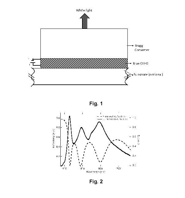
Figure 2. shows the calculated reflectivity of the WOLED as well as the
emission
spectrum of the WOLED.
As used herein, the term "low refractive index material" refers to a material
with a
refractive index of 1.65 or lower for visible wavelengths and the term "high
refractive
index material" refers to a material with a refractive index of 1.7 or higher
for visible
wavelengths.
In a specific embodiment of the present invention, the Bragg converter
comprises
alternating layers of dielectric compounds selected from the group containing
transparent oxides of silicon, tantalum, titanium, or hafnium. Non-limiting
examples
of suitable oxides include silicon oxides such as silica (silicon dioxide,
SiO2),
CA 03135366 2021-09-27
WO 2020/201633 PCT/F12020/050214
11
tantalum oxides such as tantalum pentoxide (Ta205), titanium oxides such as
titania
(TiO2), and hafnium oxides such as hafnium dioxide (Hf02).
In one embodiment of the present invention, the thickness of individual layers
of low
refractive index material is 1 nm to 100 nm, 10 nm to 90 nm, 20 nm to 80 nm,
30 nm
to 70 nm, 35 nm to 65 nm, or 40 nm to 60 nm.
In one embodiment of the present invention, the thickness of individual layers
of low
refractive index material is less than 100 nm, less than 90 nm, less than 80
nm, less
than 70 nm, less than 65 nm, or less than 60 nm.
In one embodiment of the present invention, the thickness of individual layers
of low
refractive index material is more than 1 nm, more than 10 nm, more than 20 nm,
more than 30 nm, more than 35 nm, or more than 40 nm.
In one embodiment on the present invention, the thickness of individual layers
of
low refractive index material is approximately 42 nm each. In another
embodiment
of the present invention, the thickness of individual layers of low refractive
index
material is approximately 53 nm each.
In one embodiment of the present invention, the low refractive index material
is
selected from the group containing transparent oxides of silicon. In a
specific
embodiment of the present invention, the low refractive index material is
silica
(SiO2).
In one embodiment of the present invention, the thickness of the individual
layers of
high refractive index material is 10 nm to 200 nm, 40 nm to 150 nm, 50 nm to
130
nm, 60 nm to 120 nm, 70 nm to 110 nm, 0r80 nm to 100 nm.
In one embodiment of the present invention, the thickness of the individual
layers of
high refractive index material is less than 70 nm, less than 60 nm, less than
50 nm,
less than 40 nm, less than 30 nm, or less than 25 nm.
In one embodiment of the present invention, the thickness of the individual
layers of
high refractive index material is more than 1 nm, more than 2 nm, more than 5
nm,
more than 10 nm, or more than 15 nm.
In one embodiment on the present invention, the thickness of the individual
layers
of high refractive index material is 41 nm each. In another embodiment on the
present invention, the thickness of the individual layers of high refractive
index
material is 42 nm each.
CA 03135366 2021-09-27
WO 2020/201633 PCT/F12020/050214
12
In one embodiment of the present invention, the high refractive index material
is
selected from the group containing transparent oxides of tantalum, titanium,
and
hafnium. In a specific embodiment of the present invention, the high
refractive index
material is selected from the group containing transparent oxides of tantalum.
In a
.. very specific embodiment of the present invention, the high refractive
index material
is tantalum pentoxide (Ta205).
In one embodiment of the present invention, the thickness of a pair of high
and low
refractive index layers is 30 nm to 300 nm, 45 nm to 275 nm, 50 nm to 260 nm,
60
nm to 200 nm, 70 nm to 180 nm, or 80 nm to 110 nm.
.. In one embodiment of the present invention, the thickness of a pair of high
and low
refractive index layers is less than 300 nm, less than 200 nm, less than 160
nm, less
than 100 nm, less than 120 nm, or less than 100 nm.
In one embodiment of the present invention, the thickness of a pair of high
and low
refractive index layers is more than 10 nm, more than 35 nm, more than 50 nm,
.. more than 60 nm, more than 70 nm, or more than 80 nm.
In a specific embodiment on the present invention, the thickness of a pair of
high
and low refractive index layers is 83 nm. In another specific embodiment of
the
present invention, the thickness of a pair of high and low refractive index
layers is
96 nm.
In one embodiment of the present invention the Bragg converter comprises at
least
one, at least two, at least three, at least four, or at least five layers each
comprising
a high refractive index layer and a low refractive index layer, disposed one
upon the
other. In a specific embodiment of the present invention, the Bragg converter
comprises at least six layers each comprising a high refractive index layer
and a low
.. refractive index layer, disposed one upon the other.
In one embodiment of the present invention, the total thickness of the Bragg
converter is 20 nm to 2000 nm, 30 nm to 1000 nm, 40 nm to 800 nm, 50 nm to 700
nm, 400 nm to 650 nm, or 500 nm to 600 nm.
In one embodiment of the present invention, the total thickness of the Bragg
converter is less than 2000 nm, less than 1000 nm, less than 800 nm, less than
700
nm, less than 650 nm, or less than 600 nm.
CA 03135366 2021-09-27
WO 2020/201633 PCT/F12020/050214
13
In one embodiment of the present invention, the total thickness of the Bragg
converter is more than 20 nm, more than 100 nm, more than 200 nm, more than
300 nm, more than 400 nm, or more than 500 nm.
In a specific embodiment of the present invention, the total thickness of the
Bragg
converter is approximately 498 nm. In another specific embodiment of the
present
invention, the total thickness of the Bragg converter is approximately 576 nm.
The
selection of thickness used will depend on the precise nature of the
conversion of
wavelengths needed.
It will be understood by one skilled in the art that the color of light
emitted by the
WOLED will depend on both the color emitted by the OLED and the structure of
the
Bragg converter. As a non-limiting example, it is submitted by the applicant
that in
one embodiment of the present invention, the WOLED comprising a blue OLED
according to the present disclosure emitting light with 1931 CIE coordinates
(0.19,0.15) encapsulated with a Bragg converter consisting of six layers each
comprising a high refractive index layer and a low refractive index layer,
disposed
one upon the other with a total thickness of 498 nm emits uniformly white
light with
1931 CIE coordinates (0.32,0.36). As another non-limiting example, it is
submitted
by the applicant that in one embodiment of the present invention, the WOLED
comprising a blue OLED according to the present disclosure emitting light with
1931
CIE coordinates (0.19,0.15) encapsulated with a Bragg converter consisting of
six
layers each comprising a high refractive index layer and a low refractive
index layer,
disposed one upon the other with a total thickness of 576 nm emits uniformly
white
light with 1931 CIE coordinates (0.36,0.35).
Figure 3 shows the experimentally measured emission spectrum of the OLED as
well as the experimentally measured emission spectrum from the two different
WOLEDs. Figure 3A shows the emission spectrum of a WOLED comprises a Bragg
converter with a total thickness of 498 nm and figure 3B the emission spectrum
of a
WOLED comprises a Bragg converter with a total thickness of 576 nm. In both
cases
the WOLED comprises an OLED emitting blue light with 1931 CIE coordinates
(0.19,0.15).
In one embodiment of the present invention, the WOLED comprises an OLED and
a Bragg converter. In a further embodiment, the WOLED comprises, an OLED,
Bragg converter, and a substrate.
CA 03135366 2021-09-27
WO 2020/201633 PCT/F12020/050214
14
In one embodiment of the present invention the WOLED comprises an OLED and a
Bragg converter wherein the OLED comprises an aluminium anode, a Mo03 hole-
injector, an oligofluorene emission layer, a BPhen (4,7-dipheny1-1,10-
phenanthroline) hole blocking layer, a LiF electron injection layer and an
aluminium
cathode.
In one embodiment of the present invention the WOLED comprises an OLED and a
Bragg converter wherein the OLED comprises an aluminium anode, a Mo03 hole-
injector, a TDAF (2,7-bis[9,9-di(4-methylpheny1)-fluoren-2-y1]-
9,9-di(4-
methylphenyl) fluorene) emission layer, a BPhen (4,7-dipheny1-1,10-
phenanthroline) hole blocking layer, a LiF electron injection layer and an
aluminium
cathode.
In one embodiment of the present invention, the WOLED comprises an aluminium
anode, a Mo03 hole-injector, a TDAF (2,7-bis[9,9-di(4-methylpheny1)-fluoren-2-
y1]-
9,9-di(4-methylphenyl) fluorene) emission layer, a BPhen (4,7-dipheny1-1,10-
phenanthroline) hole blocking layer, a LiF electron injection layer, an
aluminium
cathode, and a Bragg converter comprising alternating layers of SiO2 and Ta205
according to figure 4.
In one embodiment of the present invention, the WOLED comprises an aluminium
anode, a Mo03 hole-injector, a TDAF (2,7-bis[9,9-di(4-methylpheny1)-fluoren-2-
y1]-
9,9-di(4-methylphenyl) fluorene) emission layer, a BPhen (4,7-dipheny1-1,10-
phenanthroline) hole blocking layer, a LiF electron injection layer, an
aluminium
cathode, and a Bragg converter comprising alternating layers of SiO2 and Ta205
according to figure 4 arranged on a substrate.
FIG. 4 is a schematic description of a WOLED according to the present
invention.
In one embodiment of the present invention, the thickness of a WOLED according
to the present invention is 150 nm to 1350 nm, 250 nm to 1250 nm, 350 nm to
1150
nm, 450 nm to 1050 nm, 550 nm to 950 nm, or 650 nm to 850 nm.
In one embodiment of the present invention, the thickness of a WOLED according
to the present invention is less than 1350 nm, less than 1250 nm, less than
1150
nm, less than 1050 nm, less than 950 nm, or less than 850 nm.
In one embodiment of the present invention, the thickness of a WOLED according
to the present invention is more than 150 nm, more than 250 nm, more than 350
nm, more than 450 nm, more than 550 nm, or more than 650 nm.
CA 03135366 2021-09-27
WO 2020/201633 PCT/F12020/050214
In a specific embodiment of the present invention, the total thickness of the
WOLED
comprising an emission layer, a cathode, an anode, a hole injecting layer, an
electron injection layer and a Bragg converter is approximately 750 nm.
As will be understood by one skilled in the art, a WOLED according to the
present
5 invention may be manufactured in one of a number of different ways. Non-
limiting
examples of techniques for manufacturing a WOLED according to the present
invention are vacuum deposition and spin coating.
In one embodiment of the present invention, the WOLED can be constructed by
applying a mask to a suitable substrate or surface followed by sequential
vacuum
10 deposition of the material for the anode and the hole injection layer.
After the
deposition, vacuum is broken, the masking removed, and a second mask added
perpendicular to the direction of the first mask. The organic bilayer, the
electron
injection layer and the cathode layer are finally added to complete the OLED.
Once
the deposition chamber has been vented to atmospheric conditions and the
masking
15 layer has been removed, the layers of the Bragg converter are added by
sputtering
in vacuum to finalize the WOLED.
In one embodiment of the present invention, the OLED-device may be replaced
with
an inorganic LED that is a colored inorganic semiconductor that, when combined
with a Bragg converter, yields exiting light of a different color than that of
the LED.
For example, the colored inorganic semiconductors suitable for inclusion in
the
device include, but are not limited to, InGaN / GaN, ZnS, GaP:N, AlInGaP,
GaAsP,
GaAsP:N, InGaP, AlGaAs, and GaAs.
The WOLEDs of the present invention provide the additional advantage that the
use
of dielectric DBRs provide efficient encapsulation of the OLED, blocking
diffusion of
moisture and oxygen into the OLED thereby extending the lifetime of the device
significantly. This means that encapsulation of the device by e.g. epoxying is
not
necessary.
One embodiment of the present invention is a method for producing white light
with
a WOLED according to the present invention by applying electricity to the
WOLED.
In one embodiment of the present invention, the WOLED is used for producing
white
light.
CA 03135366 2021-09-27
WO 2020/201633 PCT/F12020/050214
16
Examples
The invention is described below with the help of examples. The examples are
given
only for illustrative purpose and they do not limit the scope of the
invention.
Example 1: Method for producing WOLED
The OLED fabrication was realized by using a standard vacuum evaporator with
multiple deposition sources (Edwards E306). Deposition base pressure was
approximately 10-6 mbar and the rate of deposition 2 A s-1. The OLEDs were
deposited on quartz substrates with a thickness of 1 mm. The OLEDs were
patterned in squares by using shadow masks directly in contact with the
substrates.
The bottom Al anode and Mo03 hole injection layer were deposited first and the
reactor vented to ambient atmosphere to change the mask. The top part of the
OLED consisting of TDAF, Bphen, LiF and Al was deposited and then vented to
atmospheric conditions before removing the mask. The Bragg converter was
directly
sputtered on the OLEDs.
Example 2: Characterization
A combination of ellipsometry (J.A. WooIlam M2000) and profilometry (Bruker
DektakXT) was used to determine the thin film thicknesses and obtain optical
constants. All devices were electrically characterized with a Keithley source
meter
unit (2602B). The forward spectral radiance for increasing current was
measured
with an absolute calibrated 2D CCD camera (Pixis 400) coupled to a
spectrometer
(Acton SpectrPro 2500). The pixel on the spectrometer slit was directly imaged
with
an angular aperture of 15 degrees and a magnification of 2.5. The angular-
dependent electroluminescence of the devices was obtained by collecting the
emission with an objective (10x, 0.3 NA) and by rotating the WOLED (OLED) at
the
optical axis with a goniometer. Back-focal plane objective images were then
focused
to a 200 pm spectrometer entrance slit. A vacuum micro-chamber that allows the
rotation of the devices was developed in-house. All measurements were
performed
at a base pressure of 8x10⁻² mbar. To determine the external quantum
efficiency
(EQE), the known angle-resolved EL and forward spectral radiance to correct
the
measured photon number were parametrized. EQE is then the ratio of emitted
photons to injected electrons.
Measurements showed that an OLED with thickness of approximately 160 nm
produced according to the method of Example 1 disclosure emitted light with
1931
CIE coordinates (0.19,0.15) before encapsulation with a Bragg converter.
CA 03135366 2021-09-27
WO 2020/201633 PCT/F12020/050214
17
Encapsulation of the blue OLED with a Bragg converter to produce a WOLED with
a total thickness of 498 nm yielded emitted white light with 1931 CIE
coordinates
(0.32,0.36) whereas a WOLED with a total thickness of 576 nm yielded emitted
white light with 1931 CIE coordinates (0.36,0.35).