Note: Descriptions are shown in the official language in which they were submitted.
CA 03135532 2021-09-29
WO 2020/200801 PCT/EP2020/057560
TUNABLE SUPERCONDUCTING RESONATOR FOR QUANTUM COMPUTING
DEVICES
TECHNICAL FIELD
[0001] The present invention relates generally to a superconductor device, a
fabrication
method, and fabrication system for tuning qubit coupling in superconducting
quantum
devices. More particularly, the present invention relates to a device, method,
and system for
tunable superconducting resonators for quantum computing devices.
BACKGROUND
[0002] Hereinafter, a "Q" prefix in a word or phrase is indicative of a
reference of that word
or phrase in a quantum computing context unless expressly distinguished where
used.
[0003] Molecules and subatomic particles follow the laws of quantum mechanics,
a branch
of physics that explores how the physical world works at the most fundamental
levels. At
this level, particles behave in strange ways, taking on more than one state at
the same time,
and interacting with other particles that are very far away. Quantum computing
harnesses
these quantum phenomena to process information.
[0004] The computers we use today are known as classical computers (also
referred to
herein as "conventional" computers or conventional nodes, or "CN"). A
conventional
computer uses a conventional processor fabricated using semiconductor
materials and
technology, a semiconductor memory, and a magnetic or solid-state storage
device, in what
is known as a Von Neumann architecture. Particularly, the processors in
conventional
computers are binary processors, i.e., operating on binary data represented in
1 and 0.
[0005] A quantum processor (q-processor) uses the odd nature of entangled
qubit devices
(compactly referred to herein as "qubit," plural "qubits") to perform
computational tasks. In
the particular realms where quantum mechanics operates, particles of matter
can exist in
multiple states¨such as an "on" state, an "off' state, and both "on" and "off'
states
simultaneously. Where binary computing using semiconductor processors is
limited to
using just the on and off states (equivalent to 1 and 0 in binary code), a
quantum processor
harnesses these quantum states of matter to output signals that are usable in
data computing.
1
CA 03135532 2021-09-29
WO 2020/200801 PCT/EP2020/057560
[0006] Conventional computers encode information in bits. Each bit can take
the value of 1
or 0. These is and Os act as on/off switches that ultimately drive computer
functions.
Quantum computers, on the other hand, are based on qubits, which operate
according to two
key principles of quantum physics: superposition and entanglement.
Superposition means
that each qubit can represent both a 1 and a 0 at the same time. Entanglement
means that
qubits in a superposition can be correlated with each other in a non-classical
way; that is,
the state of one (whether it is a 1 or a 0 or both) can depend on the state of
another, and that
there is more information that can be ascertained about the two qubits when
they are
entangled than when they are treated individually.
[0007] Using these two principles, qubits operate as more sophisticated
processors of
information, enabling quantum computers to function in ways that allow them to
solve
difficult problems that are intractable using conventional computers. IBM has
successfully
constructed and demonstrated the operability of a quantum processor using
superconducting
qubits (IBM is a registered trademark of International Business Machines
corporation in the
United States and in other countries.)
[0008] Superconducting devices such as qubits are fabricated using
superconducting
and semiconductor materials in known semiconductor fabrication techniques. A
superconducting device generally uses one or more layers of different
materials to
implement the device properties and function. A layer of material can be
superconductive,
conductive, semi-conductive, insulating, resistive, inductive, capacitive, or
have any number
of other properties. Different layers of materials may have to be formed using
different
methods, given the nature of the material, the shape, size or placement of the
material, other
materials adjacent to the material, and many other considerations.
[0009] Superconducting devices are often planar, i.e., where the
superconductor
structures are fabricated on one plane. A non-planar device is a three-
dimensional (3D)
device where some of the structures are formed above or below a given plane of
fabrication.
[0010] A q-processor is implemented as a set of more than one qubits. The
qubits are
fabricated as a lattice of co-planar devices on a single fabrication plane.
Such an
implementation of a q-processor is generally accepted as a fault-tolerant
quantum
architecture known as a Surface Code Scheme (SCS) or Surface Code Architecture
(SCA).
2
CA 03135532 2021-09-29
WO 2020/200801 PCT/EP2020/057560
SUMMARY
[0011] The illustrative embodiments provide a superconducting device, and a
method and
system of fabrication therefor. An embodiment of a superconducting coupling
device
includes a resonator structure. In the embodiment, the resonator structure has
a first end
configured to be coupled to a first device and a second end configured to be
coupled to a
second device. The embodiment further includes a gate positioned proximal to a
portion of
the resonator structure. In the embodiment, the gate is configured to receive
a gate voltage
and vary a kinetic inductance of the portion of the resonator based upon the
gate voltage, the
varying of the kinetic inductance inducing the resonator structure to vary a
strength of
coupling between the first device and the second device.
[0012] In another embodiment, the varying of the kinetic inductance is a
result of the gate
varying a superfluid density of the portion of the resonator structure. In
another
embodiment, the varying of the kinetic inductance induces a varying of a
characteristic
frequency of the resonator structure. In another embodiment, the varying of
the
characteristic frequency of the resonator structure enables the varying of the
strength of
coupling between the first device and the second device.
[0013] In another embodiment, at least a portion of the resonator structure is
formed of a
superconducting material comprising magic angle twisted bilayer graphene,
WTe2, Sni-s-
xInxTe, or another suitable material. In another embodiment, the gate is
formed of a metal
material or of a superconducting material.
[0014] In another embodiment, the first device is capacitively coupled to the
first end of the
resonator structure, and the second device is capacitively coupled to the
second end of the
resonator structure.
[0015] Another embodiment further includes a ground plane connected to the
resonator
structure. In another embodiment, the ground plane is connected to the
resonator structure
by a shunt portion of the resonator structure.
[0016] Another embodiment further includes a substrate structure, wherein the
resonator
structure is disposed upon a surface of the substrate structure. Another
embodiment further
includes an insulator disposed upon the resonator structure, wherein the gate
is disposed
upon the insulating structure.
3
CA 03135532 2021-09-29
WO 2020/200801 PCT/EP2020/057560
[0017] Another embodiment further includes a ground plane disposed upon the
surface of
the substrate proximate to the resonator structure.
[0018] In another embodiment, the first device is a first qubit and the second
device is a
second qubit.
[0019] In another embodiment, the first device is a qubit and the second
device includes
readout measurement circuitry of a quantum computing device.
[0020] In another embodiment, wherein the first device is a first transmon and
the second
device is a second transmon, and the resonator structure and the gate provide
tunable
coupling between the first transmon and the second transmon.
[0021] An embodiment includes a fabrication method for fabricating the
superconducting
device.
[0022] An embodiment includes a fabrication system for fabricating the
superconducting
device.
BRIEF DESCRIPTION OF THE DRAWINGS
[0023] The novel features believed characteristic of the invention are set
forth in the
appended claims. The invention itself, however, as well as a preferred mode of
use, further
objectives and advantages thereof, will best be understood by reference to the
following
detailed description of the illustrative embodiments when read in conjunction
with the
accompanying drawings, wherein:
[0024] Figure 1 depicts an example Surface Code Architecture (SCA)
illustrating a problem
that can be solved using an illustrative embodiment;
[0025] Figure 2 depicts an example gate-tunable resonator in accordance with
an illustrative
embodiment;
[0026] Figure 3 depicts an example shunted gate-tunable resonator in
accordance with an
illustrative embodiment;
[0027] Figure 4 depicts an example implementation of tuning superconducting
resonators in
an SCA arrangement in accordance with an illustrative embodiment;
[0028] Figure 5 depicts a cross-section view of a gate-tunable resonator
structure according
to an illustrative embodiment;
4
CA 03135532 2021-09-29
WO 2020/200801 PCT/EP2020/057560
[0029] Figure 6 figure depicts a cross-section view of a gate-tunable
resonator structure
according to another illustrative embodiment;
[0030] Figure 7 depicts a cross-section view of a gate-tunable resonator
structure according
to another illustrative embodiment; and
[0031] Figure 8 depicts an example implementation of tuning superconducting
resonators in
an SCA arrangement accordance with an illustrative embodiment.
DETAILED DESCRIPTION
[0032] The illustrative embodiments used to describe the invention generally
address and
solve the above-described problems and other related problems by providing a
tunable
superconducting resonator for quantum computing devices. The illustrative
embodiments
also provide a fabrication method and system for fabricating a tunable
superconducting
resonator for quantum computing devices.
[0033] Figure 1 depicts an example Surface Code Architecture (SCA)
illustrating a
problem that can be solved using an illustrative embodiment. Superconducting
qubit
architectures such as SCA 100 arrange a number of qubits 102, 102A, and 102B
in a lattice
formation on a planar two-dimensional (2D) grid. The qubits are coupled with
each other
and communicate using resonant lines 104 (also known as a "bus"). The quantum
state of a
qubit 102 is read using read lines 106 capacitively coupled to particular
qubits.
[0034] Typically, read lines 106 are resonant lines in which the qubit
state of a
particular qubit is measured using dispersive readout. Dispersive readout uses
dispersive
interaction with a resonator in which the interaction results in a dispersive
shift that causes
the frequency of the resonator to change depending on the state of the qubit.
The resonator
frequency is interrogated with a microwave pulse, typically at a frequency
near the midpoint
of the resonant frequencies corresponding to the ground and excited states.
The phase and
amplitude of the reflected signal are used to distinguish the state of the
qubit.
[0035] However, existing architectures using dispersive readout are subject
to
microwave cross-talk and/or frequency collisions between qubits resulting in
performance
degradation in quantum state measurements and correspondingly reduced
performance of
quantum computers.
CA 03135532 2021-09-29
WO 2020/200801
PCT/EP2020/057560
[0036] In
order to address the above problems with existing architectures, attempts
have been made to develop architectures to allow tuning of coupling between
qubits.
Experimentally, tuning qubit coupling has previously relied upon controlling
circuit
elements with magnetic flux. However, these flux-tunable qubits suffer from
several
disadvantages including reduced coherence times due to flux-noise, the
necessity of fine
tuning of magnetic flux, their susceptibility to on-chip cross-talk (e.g., as
high as 30%),
heating due to current needed to generate the flux, and degradation of qubit
performance
due to shortened coherence time. Some recent activity has focused on
developing voltage-
controlled tuning of qubit coupling. One recent approach toward developing
voltage-
controlled tuning has included a proposal to controllably short two grounded
transmons
through a gate-tuned semiconductor switch. Another recent approach uses a
voltage-
controlled switch based on a semiconductor nanowire to controllably ground one
end of a
superconducting cavity to change coupling of grounded gatemons.
[0037] A solution is needed to provide for tunable superconducting resonators
for quantum
computing devices to address the above-described problems related to qubit
coupling in
order to provide advantages such as reduced microwave cross-talk and/or
frequency
collisions between qubits. For example, such a solution would enable
controlling the
coupling between qubit 102A and qubit 102B in order to reduce or eliminate
microwave
cross-talk and/or frequency collisions between qubit 102A and qubit 102B
during readout or
during application of control pulses to the qubits.
[0038] An embodiment provides a tunable coupling architecture for quantum
computing
devices. An embodiment includes a gate-tunable superconducting resonator in
which a
voltage applied to a proximal gate tunes the superfluid density and kinetic
inductance in part
or all of a resonator structure coupled to qubits. Tuning the kinetic
inductance results in
tuning of a characteristic frequency of the resonator enabling adjustment of a
strength of
coupling between qubits to allow, for example, an adjustment from a weak
coupling
between qubits to a strong coupling between qubits.
[0039] Kinetic inductance is a manifestation of the inertial mass of mobile
charge carriers
as an equivalent inductance, and is observed in high carrier mobility
conductors such as
superconductors. Kinetic inductance is inversely proportional to carrier
density (or
superfluid density) such that as kinetic inductance increases, carrier density
decreases.
6
CA 03135532 2021-09-29
WO 2020/200801 PCT/EP2020/057560
[0040] In the embodiment, varying gate voltage of the metal gate results in a
varying of the
charge density. Varying of the charge density results in varying of the
kinetic inductance
and a corresponding varying of the characteristic frequency of the resonator
coupling the
qubits. Variation of the characteristic frequency of the resonator results in
a variation of the
strength of coupling between the qubits.
[0041] One or more embodiments provide for gradually tunable coupling between
nearest-
neighbor qubits via adjustment of the gate voltage. Another embodiment
provides for
multiplexed readout from qubits through tunable readout resonators. Still
another
embodiment provides for the ability to shut off qubits with unwanted
transition frequencies
by shutting off or reducing the coupling of a qubit having unwanted transition
frequencies
with one or more other qubits. One or more embodiments provide for the use of
tunable
superconducting resonators to provide a novel quantum gate hardware approach
with faster
gates and tunable coupling strength between qubits.
[0042] Another embodiment provides a fabrication method for the tunable
coupling
resonator, such that the method can be implemented as a software application.
The
application implementing a fabrication method embodiment can be configured to
operate in
conjunction with an existing superconducting fabrication system ¨ such as a
lithography
system.
[0043] For the clarity of the description, and without implying any limitation
thereto, the
illustrative embodiments are described using an example number of qubits
arranged in a
lattice. An embodiment can be implemented with a different number of qubits,
different
arrangements in a lattice, a superconducting device other than a qubit, types
of qubits not
based on superconductors, or some combination thereof, within the scope of the
illustrative
embodiments. An embodiment can be implemented to similarly improve other
superconducting fabrications where a tunable coupling to a superconducting
element is
desired.
[0044] Furthermore, a simplified diagram of the example tunable coupling
resonator is used
in the figures and the illustrative embodiments. In an actual fabrication of a
tunable
coupling resonator, additional structures that are not shown or described
herein, or
structures different from those shown and described herein, may be present
without
departing the scope of the illustrative embodiments. Similarly, within the
scope of the
illustrative embodiments, a shown or described structure in the example
tunable coupling
7
CA 03135532 2021-09-29
WO 2020/200801 PCT/EP2020/057560
resonator may be fabricated differently to yield a similar operation or result
as described
herein.
[0045] Differently shaded portions in the two-dimensional drawing of the
example
structures, layers, and formations are intended to represent different
structures, layers,
materials, and formations in the example fabrication, as described herein. The
different
structures, layers, materials, and formations may be fabricated using suitable
materials that
are known to those of ordinary skill in the art.
[0046] A specific shape, location, position, or dimension of a shape depicted
herein is not
intended to be limiting on the illustrative embodiments unless such a
characteristic is
expressly described as a feature of an embodiment. The shape, location,
position,
dimension, or some combination thereof, are chosen only for the clarity of the
drawings and
the description and may have been exaggerated, minimized, or otherwise changed
from
actual shape, location, position, or dimension that might be used in actual
lithography to
achieve an objective according to the illustrative embodiments.
[0047] Furthermore, the illustrative embodiments are described with respect to
a specific
actual or hypothetical superconducting device, e.g., a qubit, only as an
example. The steps
described by the various illustrative embodiments can be adapted for
fabricating a variety of
tunable coupling resonators in a similar manner, and such adaptations are
contemplated
within the scope of the illustrative embodiments.
[0048] An embodiment when implemented in an application causes a fabrication
process to
perform certain steps as described herein. The steps of the fabrication
process are depicted
in the several figures. Not all steps may be necessary in a particular
fabrication process.
Some fabrication processes may implement the steps in different order, combine
certain
steps, remove or replace certain steps, or perform some combination of these
and other
manipulations of steps, without departing the scope of the illustrative
embodiments.
[0049] The illustrative embodiments are described with respect to certain
types of materials,
electrical properties, structures, formations, layers orientations,
directions, steps, operations,
planes, dimensions, numerosity, data processing systems, environments,
components, and
applications only as examples. Any specific manifestations of these and other
similar
artifacts are not intended to be limiting to the invention. Any suitable
manifestation of these
and other similar artifacts can be selected within the scope of the
illustrative embodiments.
8
CA 03135532 2021-09-29
WO 2020/200801 PCT/EP2020/057560
[0050] The illustrative embodiments are described using specific designs,
architectures,
layouts, schematics, and tools only as examples and are not limiting to the
illustrative
embodiments. The illustrative embodiments may be used in conjunction with
other
comparable or similarly purposed designs, architectures, layouts, schematics,
and tools.
[0051] The examples in this disclosure are used only for the clarity of the
description and
are not limiting to the illustrative embodiments. Any advantages listed herein
are only
examples and are not intended to be limiting to the illustrative embodiments.
Additional or
different advantages may be realized by specific illustrative embodiments.
Furthermore, a
particular illustrative embodiment may have some, all, or none of the
advantages listed
above.
[0052] With reference to Figure 2, this figure depicts an example gate-tunable
resonator in
accordance with an illustrative embodiment. Top view 200 depicts a tunable
superconducting resonator structure having a resonator center conductor 202
constructed of
a superconducting material connected to a coupling pad 204 at one end and a
ground layer
210 at another end, and a metal gate 206 proximal to resonator 202.
[0053] In the particular embodiment illustrated in Figure 2, resonator center
conductor 202
is shown in a meandering configuration. In other particular embodiments,
resonator center
conductor 202 may be in a straight configuration or any other suitable
resonator
configuration. In the illustrated embodiment, metal gate 206 is of a planar
rectangular
shape and positioned below and proximate to substantially the entire length of
resonator
center conductor 202. In other particular embodiments, metal gate 206 may be
of any
suitable shape, size, or configuration. In other embodiments, other gate and
qubit structures
may be used, and the gate structure may not gate the entire resonator center
conductor 202
but may only gate a portion of the resonator center conductor 202. In other
embodiments,
more than one qubit may be capacitively coupled to the resonator center
conductor 202 at
different locations along its length. In one or more embodiments, resonator
center
conductor 202 and metal gate 206 are separated by an insulator material or a
vacuum. In an
embodiment, metal gate 206 may overlap only part of the resonator instead of
substantially
its entire length.
[0054] In some embodiments, the ground layer 210 may be constructed in such a
way that
the resonator comprises a coplanar waveguide. In this geometry, the ground
plane is
separated from the resonator center conductor 202 on either side by a distance
which does
9
CA 03135532 2021-09-29
WO 2020/200801 PCT/EP2020/057560
not vary along the length of the resonator. The dimensions are typically
guided by design
specifications for a transmission line with 50 ohm impedance in the frequency
regime of 1
M1Hz-20 GHz. In the embodiment illustrated in Figure 2, this ground plane
geometry is not
shown for clarity.
[0055] In particular embodiments, possible superconducting materials of which
resonator
center conductor 202, coupling pad 204, gate 206, or ground layer 210 may be
formed
include one or more of aluminum, indium, niobium, niobium nitride, niobium
titanium
nitride, niobium diselenide, tantalum, titanium, or molybdenum rhenium. In
particular
embodiments, possible metallic or conductive gate materials of which metal
gate 206 may
be formed include gold, platinum, palladium, gold alloys (e.g. palladium
gold), copper, or
graphite It should be understood that the foregoing is a non-exhaustive list
of possible
superconducting materials and metallic materials, and in other embodiments
other suitable
superconducting materials or metallic materials may be used. In some
embodiments, the
resonator may only be partially composed of a gate-tunable superconductor
material and
other portions of the resonator may be composed materials that are not gate-
tunable.
Coupling pad 204 is configured to capacitively couple a qubit 208 to resonator
center
conductor 202.
[0056] In an embodiment, a gate voltage Vgate is applied to metal gate 206 to
cause a
controllable variation in carrier density within resonator center conductor
202, and thereby
further cause a variation in kinetic inductance of resonator center conductor
202 as the
kinetic inductance Lk of resonator center conductor 202 is inversely
proportional to the
carrier density ns. The variation in kinetic inductance Lk further causes a
change in the
characteristic frequency of the resonator comprising center conductor 202,
which further
changes the strength of coupling between qubit 208 and the other device.
Accordingly, the
gate voltage Vgate is configurable to tune the kinetic inductance Lk and hence
capable of
detuning the resonator comprising center conductor 202 to change the strength
of coupling
between qubit 208 and the other device.
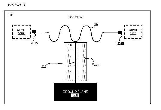
[0057] With reference to Figure 3, this figure depicts an example shunted gate-
tunable
resonator in accordance with an illustrative embodiment. Top view 300 depicts
a shunted
tunable superconducting resonator structure having a resonator center
conductor 302
constructed of a superconducting material connected to a first coupling pad
304A at one end
and a second coupling pad 304B at another end. Resonator center conductor 302
is
CA 03135532 2021-09-29
WO 2020/200801 PCT/EP2020/057560
connected to a shunt portion 312 coupling resonator center conductor 302 to a
ground plane
308. In an embodiment, resonator center conductor 302 and shunt portion 312
may be
composed of a continuous piece of the same superconducting material. A metal
gate 306 is
proximal to the shunt portion 312. In a particular embodiment, ground plane
308 is a
superconducting ground plane formed of a superconducting material. In other
embodiments, other gate and qubit structures may be used, and the gate
structure may gate
all or part of the resonator center conductor 302 and/or all or part of the
shunt 312.
[0058] In some embodiments, the ground layer 308 may be constructed in such a
way that
the resonator comprises a coplanar waveguide. In this geometry, the ground
plane is
separated from the resonator center conductor 302, as well as the shunt 312,
on either side
by a distance which does not vary along the length of the resonator. The
dimensions are
typically guided by design specifications for a transmission line with 50 ohm
impedance in
the frequency regime of 1 1V1Hz-20 GHz. In the embodiment illustrated in
Figure 3, this
ground plane geometry is not shown for clarity.
[0059] In the particular embodiment illustrated in Figure 3, resonator center
conductor 302
is shown in a meandering configuration. In other particular embodiments,
resonator center
conductor 302 may be in a straight configuration or any other suitable
resonator
configuration. In the illustrated embodiment, metal gate 306 is of a planar
rectangular
shape and positioned proximate to substantially the entire length of the shunt
portion 312. In
other particular embodiments, metal gate 306 may be of any suitable shape,
size, or
configuration. In one or more embodiments, resonator center conductor 302 and
metal gate
306 are separated by an insulator material or a vacuum.
[0060] First coupling pad 304A is configured to capacitively couple a first
qubit 310A to
resonator center conductor 302, and second coupling pad 304B is configured to
capacitively
couple a second qubit 310B to resonator center conductor 302. In some
embodiments, first
coupling pad 304A is configured to capacitively couple a qubit 310A to
resonator center
conductor 302, and second coupling pad 304B is configured to capacitively
couple to
another device such as readout measurement circuitry. In some embodiments,
first coupling
pad 304A is configured to capacitively couple a qubit 310A to resonator center
conductor
302, and second coupling pad 304B couples directly to readout measurement
circuitry, for
example using a wirebond or bump bond.
11
CA 03135532 2021-09-29
WO 2020/200801 PCT/EP2020/057560
[0061] In an embodiment, a gate voltage Vgate is applied to metal gate 306 to
cause a
controllable variation in carrier density within resonator center conductor
302, and thereby
further cause a variation in kinetic inductance of resonator center conductor
302 as the
kinetic inductance Lk of resonator center conductor 302 is inversely
proportional to the
carrier density ns. The variation in kinetic inductance Lk further causes a
change in the
characteristic frequency of the resonator comprising center conductor 302,
which further
changes the strength of coupling between first qubit 310A and second qubit
310B.
Accordingly, the gate voltage Vgate is configurable to tune the kinetic
inductance Lk and
hence capable of detuning the resonator comprising center conductor 302 to
change the
strength of coupling between first qubit 310A and second qubit 310B.
[0062] With reference to Figure 4, this figure depicts an example
implementation of tuning
superconducting resonators in an SCA arrangement accordance with an
illustrative
embodiment. Top view 400 depicts a number of qubits 402 in a lattice formation
on a
planar two-dimensional (2D) grid. The qubits are coupled with each other and
communicate using resonant lines 404 (also known as a "bus"). The quantum
state of a
qubit 102 is read using read lines 406, 406A capacitively coupled to
particular qubits. Each
of read lines 406A further include a metal gate 408 disposed proximate thereto
to form a
gate-tunable resonator such as described herein with respect to various
embodiments.
[0063] In the illustrated embodiment, each of read lines 406A and the
corresponding metal
gate 408 forming a gate-tunable resonator are configured to receive an
individually
controllable gate voltage to allow controlled coupling and decoupling of a
particular qubit
402 from a read line 406. In one or more embodiments, the individually gated
sections of
gate-tunable resonators provide for the capability of multiplexed readout of
qubits 406
through tunable readout resonators.
[0064] With reference to Figure 5, this figure depicts a cross-section view of
a gate-tunable
resonator structure 500 according to an illustrative embodiment. Structure 500
includes a
substrate structure 502 having superconducting ground plane portions 504
formed on a
surface (e.g., a top surface) of substrate structure 502. In particular
embodiments, substrate
structure 502 can be formed of any suitable substrate material, such as
silicon (Si) or
sapphire. Structure 500 further includes a resonator center conductor 506
disposed on the
surface of substrate structure 502 proximate to superconducting ground plane
portions 504.
Together the resonator center conductor 506 and superconducting ground plane
portions
12
CA 03135532 2021-09-29
WO 2020/200801 PCT/EP2020/057560
504 comprise a coplanar waveguide resonator. In some embodiments, the
dimensions and
location of components in structure 500 may be designed to account for
capacitance due to
the gate 510.
[0065] In the embodiment illustrated in Figure 5, resonator center conductor
506 is formed
of magic-angle twisted bilayer graphene (MATBG) material as a superconducting
material.
In particular embodiments, the MATBG material is tuned to a superconducting
critical
temperature I', between 0 kelvin (K) and 1.7 K.
[0066] Structure 500 further includes an insulator layer or vacuum region 508
separating
resonator center conductor 506 and a metal gate 510. In one or more
embodiments,
structure 500 is an example of a gate-tunable resonator such as those
described with respect
to Figures 2-4. In one or more embodiments, resonator center conductor 506 is
capacitively
coupled between two superconducting devices such as first qubit 310A and
second qubit
310B of Figure 3. In some embodiments, the structure 500 represents a cross-
section view
through structure 202, structure 302, and/or structure 306.
[0067] In an embodiment, a gate voltage Vgate is applied to metal gate 510 to
cause a
controllable variation in carrier density within resonator center conductor
506, and thereby
further cause a variation in kinetic inductance of resonator center conductor
506 as the
kinetic inductance Lk of resonator center conductor 506 is inversely
proportional to the
carrier density ns. The variation in kinetic inductance Lk further causes a
change in the
characteristic frequency of the resonator in structure 500, which further
changes the strength
of coupling between first qubit 310A and second qubit 310B. Accordingly, the
gate voltage
Vgate is configurable to tune the kinetic inductance Lk and hence capable of
tuning the
resonator in structure 500 to change the strength of coupling between first
qubit 310A and
second qubit 310B.
[0068] With reference to Figure 6, this figure depicts a cross-section view of
a gate-tunable
resonator structure 600 according to another illustrative embodiment.
Structure 600
includes a substrate structure 602 having superconducting ground plane
portions 604
formed on a surface (e.g., a top surface) of substrate structure 602. In
particular
embodiments, substrate structure 602 can be formed of any suitable substrate
material, such
as silicon (Si) or sapphire. Structure 600 further includes a resonator center
conductor 606
formed of a superconducting material disposed on the surface of substrate
structure 602
proximate to superconducting ground plane portions 604. Together the resonator
center
13
CA 03135532 2021-09-29
WO 2020/200801 PCT/EP2020/057560
conductor 606 and superconducting ground plane portions 604 comprise a
coplanar
waveguide resonator. In some embodiments, the dimensions and location of
components in
structure 600 may be designed to account for capacitance due to the gate 610.
[0069] In the embodiment illustrated in Figure 6, resonator center conductor
606 is formed
of tungsten ditelluride (WTe2) material as a superconducting material. In
particular
embodiments, the WTe2material is tuned to a superconducting critical
temperature I',
between 0 K and 0.61 K.
[0070] Structure 600 further includes an insulator layer or vacuum region 608
separating
resonator center conductor 606 and a metal gate 610. In one or more
embodiments,
structure 600 is an example of a gate-tunable resonator such as those
described with respect
to Figures 2-4. In one or more embodiments, resonator center conductor 606 is
capacitively
coupled between two superconducting devices such as first qubit 310A and
second 310B of
Figure 3. In some embodiments, structure 600 represents a cross-section view
through
structure 202, structure 302, and/or structure 306.
[0071] In an embodiment, a gate voltage Vgate is applied to metal gate 610 to
cause a
controllable variation in carrier density within resonator center conductor
606, and thereby
further cause a variation in kinetic inductance of resonator center conductor
606 as the
kinetic inductance Lk of resonator center conductor 606 is inversely
proportional to the
carrier density ns. The variation in kinetic inductance Lk further causes a
change in the
characteristic frequency of the resonator in structure 600, which further
changes the strength
of coupling between first qubit 310A and second qubit 310B. Accordingly, the
gate voltage
Vgate is configurable to tune the kinetic inductance Lk and hence capable of
tuning the
resonator in structure 600 to change the strength of coupling between first
qubit 310A and
second qubit 310B.
[0072] With reference to Figure 7, this figure depicts a cross-section view of
a gate-tunable
resonator structure 700 according to another illustrative embodiment.
Structure 700
includes a substrate structure 702 having superconducting ground plane
portions 704
formed on a surface (e.g., a top surface) of substrate structure 702. In
particular
embodiments, substrate structure 702 can be formed of any suitable substrate
material, such
as silicon (Si) or sapphire. Structure 700 further includes a resonator center
conductor 706
formed of a superconducting material disposed on the surface of substrate
structure 702
proximate to superconducting ground plane portions 704. Together the resonator
center
14
CA 03135532 2021-09-29
WO 2020/200801 PCT/EP2020/057560
conductor 706 and superconducting ground plane portions 704 comprise a
coplanar
waveguide resonator. In some embodiments, the dimensions and location of
components in
structure 700 may be designed to account for capacitance due to the gate 710.
[0073] In the embodiment illustrated in Figure 7, resonator center conductor
706 is formed
of a thin layer of SniInxTe material as a superconducting material.
[0074] Structure 700 further includes an insulator layer or vacuum region 708
separating
resonator center conductor 706 and a metal gate 710. In one or more
embodiments,
structure 700 is an example of a gate-tunable resonator such as those
described with respect
to Figures 2-4. In one or more embodiments, resonator center conductor 706 is
capacitively
coupled between two superconducting devices such as first qubit 310A and
second 310B of
Figure 3. In some embodiments, the structure 700 represents a cross-section
view through
structure 202, structure 302, and/or structure 306.
[0075] In an embodiment, a gate voltage Vgate is applied to metal gate 710 to
cause a
controllable variation in carrier density within resonator center conductor
706, and thereby
further cause a variation in kinetic inductance of resonator center conductor
706 as the
kinetic inductance Lk of resonator center conductor 706 is inversely
proportional to the
carrier density ns. The variation in kinetic inductance Lk further causes a
change in the
characteristic frequency of the resonator in structure 700, which further
changes the strength
of coupling between first qubit 310A and second qubit 310B. Accordingly, the
gate voltage
Vgate is configurable to tune the kinetic inductance Lk and hence capable of
tuning the
resonator in structure 700 to change the strength of coupling between first
qubit 310A and
second qubit 310B.
[0076] With reference to Figure 8, this figure depicts an example
implementation of tuning
superconducting resonators in an SCA arrangement accordance with an
illustrative
embodiment. Top view 800 depicts a number of qubits 802 in a lattice formation
on a
planar two-dimensional (2D) grid. The quantum state of a qubit 802 is read
using read lines
806 capacitively coupled to particular qubits. The qubits are coupled with
each other and
communicate using resonant lines 804 (also known as a "bus"). Each of resonant
lines 804
further include a gate 808 disposed proximate thereto to form a gate-tunable
resonator such
as described herein with respect to various embodiments.
[0077] In the illustrated embodiment, each of resonant lines 804 and the
corresponding gate
808 forming a gate-tunable resonator are configured to receive an individually
controllable
CA 03135532 2021-09-29
WO 2020/200801 PCT/EP2020/057560
gate voltage to allow controlled coupling and decoupling of pairs of qubits
802. In one or
more embodiments, the individually gated sections of gate-tunable resonators
provide for
the capability of gradually tuning coupling between nearest-neighbor qubits.
In one or more
embodiments, the individually gated sections of gate-tunable resonators
provide for the
capability of shutting off qubits with unwanted transition frequencies. In one
or more
embodiments, the individually gated sections of gate-tunable resonators
provide for a novel
quantum gate hardware approach with faster gates and tunable coupling strength
between
qubits.
[0078] Various embodiments of the present invention are described herein with
reference to
the related drawings. Alternative embodiments can be devised without departing
from the
scope of this invention. Although various connections and positional
relationships (e.g.,
over, below, adjacent, etc.) are set forth between elements in the following
description and
in the drawings, persons skilled in the art will recognize that many of the
positional
relationships described herein are orientation-independent when the described
functionality
is maintained even though the orientation is changed. These connections and/or
positional
relationships, unless specified otherwise, can be direct or indirect, and the
present invention
is not intended to be limiting in this respect. Accordingly, a coupling of
entities can refer to
either a direct or an indirect coupling, and a positional relationship between
entities can be a
direct or indirect positional relationship. As an example of an indirect
positional
relationship, references in the present description to forming layer "A" over
layer "B"
include situations in which one or more intermediate layers (e.g., layer "C")
is between
layer "A" and layer "B" as long as the relevant characteristics and
functionalities of layer
"A" and layer "B" are not substantially changed by the intermediate layer(s).
[0079] The following definitions and abbreviations are to be used for the
interpretation of
the claims and the specification. As used herein, the terms "comprises,"
"comprising,"
"includes," "including," "has," "having," "contains" or "containing," or any
other variation
thereof, are intended to cover a non-exclusive inclusion. For example, a
composition, a
mixture, process, method, article, or apparatus that comprises a list of
elements is not
necessarily limited to only those elements but can include other elements not
expressly
listed or inherent to such composition, mixture, process, method, article, or
apparatus.
[0080] Additionally, the term "illustrative" is used herein to mean "serving
as an example,
instance or illustration." Any embodiment or design described herein as
"illustrative" is not
16
CA 03135532 2021-09-29
WO 2020/200801 PCT/EP2020/057560
necessarily to be construed as preferred or advantageous over other
embodiments or
designs. The terms "at least one" and "one or more" are understood to include
any integer
number greater than or equal to one, i.e. one, two, three, four, etc. The
terms "a plurality"
are understood to include any integer number greater than or equal to two,
i.e. two, three,
four, five, etc. The term "connection" can include an indirect "connection"
and a direct
"connection."
[0081] References in the specification to "one embodiment," "an embodiment,"
"an
example embodiment," etc., indicate that the embodiment described can include
a particular
feature, structure, or characteristic, but every embodiment may or may not
include the
particular feature, structure, or characteristic. Moreover, such phrases are
not necessarily
referring to the same embodiment. Further, when a particular feature,
structure, or
characteristic is described in connection with an embodiment, it is submitted
that it is within
the knowledge of one skilled in the art to affect such feature, structure, or
characteristic in
connection with other embodiments whether or not explicitly described.
[0082] The terms "about," "substantially," "approximately," and variations
thereof, are
intended to include the degree of error associated with measurement of the
particular
quantity based upon the equipment available at the time of filing the
application. For
example, "about" can include a range of 8% or 5%, or 2% of a given value.
[0083] The descriptions of the various embodiments of the present invention
have been
presented for purposes of illustration, but are not intended to be exhaustive
or limited to the
embodiments disclosed. Many modifications and variations will be apparent to
those of
ordinary skill in the art without departing from the scope and spirit of the
described
embodiments. The terminology used herein was chosen to best explain the
principles of the
embodiments, the practical application or technical improvement over
technologies found in
the marketplace, or to enable others of ordinary skill in the art to
understand the
embodiments described herein.
17