Note: Descriptions are shown in the official language in which they were submitted.
CA 03137719 2021-10-21
WO 2020/219857
PCT/US2020/029784
MOTOR DRIVE TOPOLOGIES FOR TRACTION AND CHARGING
IN ELECTRIFIED VEHICLES
CROSS-REFERENCE TO RELATED APPLICATIONS
[0001] This PCT International Patent Application claims the benefit of
and priority
to U.S. Provisional Patent Application Serial No. 62/838,538, filed April 25,
2019, titled
"Motor Drive Topologies For Electrified Vehicles," and U.S. Provisional Patent
Application Serial No. 62/861,020, filed June 13, 2019, titled "Inverter For
Electric Motor
Drive," the entire disclosures of these applications are hereby incorporated
by reference.
FIELD
[0002] The present disclosure relates generally to inverters for
converting direct
current (DC) electrical power to alternating current (AC). More specifically,
the present
disclosure relates to such inverters for use in motor drive systems to power
traction motors
in electrified vehicles and to convert AC to DC for regenerative braking and
charging a
battery pack.
BACKGROUND
[0003] Inverters are electrical devices used to convert direct current
(DC) electrical
power to alternating current (AC) and vice-versa. One specific application of
inverters is in
electric motor drives, also known as variable frequency drives (VFDs) that are
used in a
variety of applications to provide alternating current (AC) electrical power
to an electric
motor. Motor drives including inverters are frequently used for powering
traction motors in
electric vehicles (EVs), such as battery electric vehicles, hybrid electric
vehicles (HEVs),
and plug-in hybrid electric vehicles (PHEVs). It is desirable to improve
efficiency of a
traction drive system that includes both the motor drive and the electric
motor to reduce
energy consumption from the vehicle's battery and to extend driving range.
1
CA 03137719 2021-10-21
WO 2020/219857
PCT/US2020/029784
[0004] Conventional electric motor drives generally rely upon solid-
state switches
to switch a battery via pulse width modulation (PWM) in order to approximate
an
alternating current waveform on one or more output terminals providing power
to the
electric motor. Historically, insulated gate bipolar transistors (IGBTs) or
metal-oxide-
semiconductor field-effect transistors (MOSFETs) are used as the switches.
Conventional
switching transistors using a silicon substrate have a bandgap of 1.1 electron-
volt (eV).
Conventional switching transistors are not generally able to operate at more
than 10 kHz to
switch the high electrical currents required for motor drive applications.
[0005] Wide-bandgap (WBG) devices, such as Silicon carbide (SiC)
transistors or
Gallium nitride (GaN) transistors have been used recently in motor drive
applications to
provide high switching frequency operation, with reduced form factor,
switching losses and
reduced motor harmonic loss and DC bus ripple. Costs of the WBG devices are
relatively
high when compared with conventional solid-state switches such as silicon
IGBTs or
MOSFETs, which increases the inverter cost. High frequency operation of the
motor drive
can trigger parasitic components present at the bus bar, across the power
electronic device
and device module with respect to ground, which causes additional disturbances
in the
voltage and current waveforms as electromagnetic interference (EMI). Due to
pulse width
modulation (PWM) and parasitic components, conventional inverters generate
common
mode noise with respect to the ground. Also, the common mode voltage causes a
shaft
voltage in a shaft of a motor connected to the motor drive. Such shaft voltage
can cause
bearing currents when the shaft voltage exceeds a breakdown voltage level of
the bearing
grease in the motor. Passive filters are traditionally used at the input or
output of the
inverter to minimize these issues. However, passive filters increase cost,
loss, volume and
weight of the system.
2
CA 03137719 2021-10-21
WO 2020/219857
PCT/US2020/029784
[0006] In some applications, electric motor drives may also be used to
convert AC
power to DC power for charging a battery pack in a vehicle. The AC power may
be
supplied by the electric motor, for example, in a regenerative braking mode.
Alternatively
or additionally, the AC power may be supplied by an external source, such as a
fixed
charging station attached to the utility power grid.
SUMMARY
[0007] According to some embodiments, an inverter for converting between
direct
current (DC) and alternating current (AC) power includes a phase driver
configured to
switch current from the DC source to generate the AC power upon an output
terminal. The
phase driver includes a first solid-state switch having a first voltage rating
and a second
solid-state switch having a second voltage rating higher than the first
voltage rating.
BRIEF DESCRIPTION OF THE DRAWINGS
[0008] Further details, features and advantages of designs of the
invention result
from the following description of embodiment examples in reference to the
associated
drawings.
[0009] FIG. 1 is a block diagram of a first motor drive system in
accordance with
some embodiments of the present disclosure;
[0010] FIG. 2 is a block diagram of a second motor drive system in
accordance with
some embodiments of the present disclosure;
[0011] FIG. 3 is a block diagram of a third motor drive system in
accordance with
some embodiments of the present disclosure;
[0012] FIG. 4 is a schematic diagram of a motor drive in accordance with
some
embodiments of the present disclosure;
[0013] FIG. 5 is a schematic diagram of a motor drive in accordance with
some
embodiments of the present disclosure;
3
CA 03137719 2021-10-21
WO 2020/219857
PCT/US2020/029784
[0014] FIG. 6 is a schematic diagram of a motor drive in accordance with
some
embodiments of the present disclosure;
[0015] FIG. 7 is a schematic diagram of a motor drive in accordance with
some
embodiments of the present disclosure;
[0016] FIG. 8 is a schematic diagram of a motor drive including a nine-
switch
inverter in accordance with some embodiments of the present disclosure;
[0017] FIG. 9 is a schematic diagram of a motor drive including a two-
level
inverter;
[0018] FIG. 10 is a schematic diagram of a motor drive including a nine-
switch
inverter in accordance with some embodiments of the present disclosure;
[0019] FIG. 11 is a schematic diagram of a motor drive including a nine-
switch
inverter in accordance with some embodiments of the present disclosure;
[0020] FIG. 12 is a schematic diagram of a motor drive in accordance
with some
embodiments of the present disclosure;
[0021] FIG. 13 is a schematic diagram of solid-state switches with gate
driver
circuits in accordance with some embodiments of the present disclosure;
[0022] FIG. 14 is a schematic diagram showing different switching states
of a three-
phase inverter;
[0023] FIG. 15 is a graph showing inverter output voltage space vectors;
and
[0024] FIG. 16 is a graph showing inverter output voltage space vectors
with near-
state control sectors.
DETAILED DESCRIPTION
[0025] Recurring features are marked with identical reference numerals
in the
figures, in which example embodiments of an electric motor drive system 10 are
is
disclosed.
4
CA 03137719 2021-10-21
WO 2020/219857
PCT/US2020/029784
[0026] In some embodiments, and as shown in the block diagrams of FIGS.
1-3, the
motor drive system 10 operates as a current source inverter (CSI), which is
configured to
supply a relative constant electrical current. Details of the operation of the
motor drive
system are explained below.
[0027] Current source inverters (CSI) offer several advantages over
voltage source
inverters (VSI) used in conventional motor drives, particularly when used with
wide
bandgap (WBG) based switches. For example, high switching frequency of WBG
devices
may allow for reduced sizing of inductive components in the CSI when compared
with CSI
designs that use conventional silicon-based (Si) devices for switching.
[0028] Advantages of using a CSI include, improved efficiency of the
motor drive
system 10, as a result of high switching frequency and high switching speeds
of WBG
switches, while also reducing electromagnetic interference (EMI) when compared
with
conventional VSI designs. Specifically, a CSI may provide attenuated EMI
because the CSI
includes a DC bus inductor, which serves as a low-pass filter to suppress
common-mode
current. This can provide substantial improvements over conventional VSI
designs, such as
a 2 level VSI with 6 WBG switches, especially when operating at high
frequencies, which
otherwise may require very large EMI filters to reduce electromagnetic
interference (EMI)
and dv/dt at the motor terminals. Such large EMI filters can add weight and
cost such that
they may be unfeasible for use in electrified vehicles. For example, an EMI
filter designed
for a VSI with an operating frequency of 200 kHz was 23 times larger than one
designed for
20 kHz.
[0029] Another advantage of using a CSI over a VSI pertains to DC link
capacitors:
conventional VSI designs typically include a DC link capacitor at the input.
DC link
capacitors size can be decreased up to a threshold switching frequency, above
which the
capacitor size does not decrease much as it is designed based on the root-mean
square
CA 03137719 2021-10-21
WO 2020/219857
PCT/US2020/029784
(RMS) current rating instead of its capacitance. Hence, VSI designs may not be
able to
realize power density improvements that are theoretically possible. Another
advantage of
using a CSI over a VSI is for fault tolerance: the DC bus inductor of a CSI
naturally limits
the rate of fault current increases, giving the CSI a long-acknowledged
advantage in fault
robustness compared to VSIs.
[0030] Another advantage of using a CSI over a VSI pertains to output
voltage: A
CSI may produce an output voltage waveform of the CSI that is nearly
sinusoidal with
minimal ripple due to the presence of output filter capacitors. Such a high-
quality output
voltage waveform helps to reduce losses and reduces dv/dt in the electric
motor. The high-
quality output voltage output waveform may also reduce deterioration and
failure in the
insulation within the electric motor, and may allow the drive system 10 to be
used with
electric motors having reduced winding insulation when compared with electric
motors
designed to withstand high dv/dt from use with a conventional VSI. Another
advantage of
using a CSI over a VSI pertains to Boost capability: a CSI can provide the
capability to
boost the output voltage to a higher level than the source voltage. This may
enable the
electric motor to operate at higher base speed and/or with a higher constant
power region.
[0031] Referring to FIG. 1, a block diagram showing a motor drive system
10
having a first configuration 12 is provided. The motor drive system 10 may be
used within
an electrified vehicle, such as battery electric vehicle (EV) or a plug-in
hybrid electric
vehicle (PHEV). The motor drive system 10 is configured to provide AC power to
an
electric motor 32, which is operable in a traction mode to transmit torque to
wheels 34 for
propelling the electrified vehicle. In some embodiments, the electric motor 32
may be a
motor/generator (M/G), which is operable as either a motor or as a generator
to generate
electrical current. The motor drive system 10 includes a battery bus 22 for
connection to a
battery 20 including one or more battery cells or groups of battery cells. In
some
6
CA 03137719 2021-10-21
WO 2020/219857
PCT/US2020/029784
embodiments, one or more other storage devices or systems capable of supplying
direct
current (DC) electrical power, such as super-capacitors may be used instead of
or in
addition to the battery 20. The battery bus 22 includes a positive source node
22a and a
reference source node 22b and is configured to provide a first DC electrical
power having a
substantially constant voltage.
[0032] The motor drive system 10 also includes a voltage-to-current (V-
I) converter
24, which is operable in the traction mode to receive the first DC electrical
power from the
battery bus 22 and to supply a second DC electrical power having a
substantially constant
current upon a DC link bus 26 including a high-side conductor 26a and a low-
side
conductor 26b. The motor drive system 10 also includes a current-source
inverter (CSI) 28,
which may also be called an inverter bridge 28, including a plurality of solid-
state switches
configured to generate an AC power upon one or more motor leads 30 by
selectively
switching the second DC electrical power from the DC link bus 26. The inverter
bridge 28
may also function to rectify AC power from the one or more motor leads 30 to
supply DC
electrical power to the DC link bus 26 for charging the battery 20.
[0033] In some embodiments, the V-I converter 24 is operable in a
charging mode
to receive power from the DC link bus 26 and to supply power to the battery
bus 22 to the
battery 20 connected thereto. For example, FIG. 2 shows a block diagram of the
motor drive
system 10 having a second configuration 12', in which an alternating current
(AC) supply
36 is connected to windings of the electric motor 32 in order to energize the
motor leads 30.
The AC supply 36 may be an external supply, such as a fixed charging station
or utility grid
supply providing AC power to the electrified vehicle. The AC supply 36 is
shown as a 3-
phase supply having three power conductors, however, the AC supply 36 may have
other
configurations such as a single-phase configuration.
7
CA 03137719 2021-10-21
WO 2020/219857
PCT/US2020/029784
[0034] Alternatively or additionally, the motor drive system 10 may
operate in a
regenerative mode to convert AC power induced in the windings of the electric
motor 32 to
supply power to the battery 20. Such a regenerative mode may operate similarly
to the
second configuration 12' shown in FIG. 2, except with power being transferred
from the
wheels 34 to the electric motor 32, and without the external AC supply 36. In
some
embodiments, and as shown in FIG. 3, a DC supply 38 may be coupled to the DC
link bus
26 to supply DC electrical current, which may be used to charge the battery
20.
[0035] In some embodiments, each of the solid-state switches in the
inverter bridge
28 are wide-bandgap (WBG) devices having a bandgap greater than 2.0 electron-
volts (eV).
In some embodiments, each of the solid-state switches in the inverter bridge
28 may have a
bandgap of between 2 and 4 electron-volts (eV). For example, each of the solid-
state
switches in the inverter bridge 28 may be Silicon carbide (SiC) transistors,
which may have
a bandgap of 2.36 to 3.24 eV, with different polytypes of SiC having different
bandgaps. In
another example, each of the solid-state switches in the inverter bridge 28
may be Gallium
nitride (GaN) transistors, which may have a bandgap of about 3.4 eV.
[0036] In some embodiments, the V-I converter 24 may be configured to
boost a
first DC voltage from the DC link bus to a second DC voltage upon the battery
bus 22 in the
charging mode, with the second DC voltage greater than the first DC voltage.
More
specifically, the inverter bridge 28 and the V-I converter 24 may operate in
conjunction
with one-another to boost the voltage on the DC link bus 26 to a higher
voltage on the
battery bus 22. In some embodiments, the second DC voltage may be at least two-
times the
first DC voltage. For example, the DC link bus 26 may have a first voltage of
400 VDC,
which may be boosted to a second voltage of 800VDC upon the battery bus 22,
which may
be determined to match the operating requirements of the battery 20.
8
CA 03137719 2021-10-21
WO 2020/219857
PCT/US2020/029784
[0037] In some embodiments, and shown in the example schematic diagrams
of
FIGS. 4-7, the V-I converter 24 includes a quasi-Z-Source (qZS).
[0038] Referring to FIGS. 4-7, schematic diagrams of different example
configurations of a motor drive system 10 are shown. More specifically, the
motor drive
systems 10 shown in FIGS. 4-7 each include a V-I converter 24 with a quasi-Z-
Source
(qZS) that includes a DC Bus inductor 50 defining a first lead and a second
lead, with the
first lead connected to the positive source node 22a of the battery bus 22.
The motor drive
systems 10 shown in FIGS. 4-7 each also include a first winding 52 defining a
first lead and
a second lead, a second winding 54 defining a first lead and a second lead, a
first capacitor
56 defining a first terminal and a second terminal. The motor drive systems 10
shown in
FIGS. 4-7 each also include a rectifier 58 defining an input terminal and an
output terminal
and configured to pass current from the input terminal to the output terminal
while blocking
current from passing in an opposite direction.
[0039] In some embodiments, and as shown in FIGS. 4-7, the motor drive
system 10
may include an output choke 60 including capacitors connected between each of
the motor
leads 30 and a common node, which may be connected to an earth ground. The
output
choke 60 may function to reduce electromagnetic interference (EMI) from being
transmitted
to the motor leads 30 from the inverter bridge 28. The output choke 60 may
also control
oscillating torque and V and I waveform symmetry and shape in the electric
motor 32
during charging.
[0040] Referring now to the example motor drive system 10 of FIG. 4,
each of the
first winding 52 and the second winding 54 are inductors. The reference source
node 22b of
the battery bus 22 is connected to the low-side conductor 26b of the DC link
bus 26. The
second lead of the DC bus inductor 50 is connected to the high-side conductor
26a of the
DC link bus 26 and to the first lead of the first winding 52. The second lead
of the first
9
CA 03137719 2021-10-21
WO 2020/219857
PCT/US2020/029784
winding 52 defines a first internal node 64. The first terminal of the first
capacitor 56 is
connected to the first internal node 64, and the second terminal of the first
capacitor 56 is
connected to the low-side conductor 26b of the DC link bus 26. The output
terminal of the
rectifier 58 connected to the first internal node 64, and the input terminal
of the rectifier 58
defines a second internal node 66. The example V-I converter 24 of FIG. 4 also
includes a
second capacitor 62 defining a first terminal and a second terminal, with the
first terminal of
the second capacitor 62 connected to the high-side conductor 26a of the DC
link bus 26,
and the second terminal of the second capacitor 62 connected to the second
internal node
66. The first lead of the second winding 54 is connected to the second
internal node 66, and
the second lead of the second winding 54 is connected to the low-side
conductor 26b of the
DC link bus 26.
[0041] Referring now to the example motor drive system 10 of FIG. 5,
each of the
first winding 52 and the second winding 54 are inductors. The second lead of
the DC bus
inductor 50 defines a first internal node 64. The first lead of the first
winding 52 is
connected to the first internal node 64, and the second lead of the first
winding 52 is
connected to the high-side conductor 26a of the DC link bus 26. The first
terminal of the
first capacitor 56 is connected to the first internal node 64, and the second
terminal of the
first capacitor 56 is connected to the low-side conductor 26b of the DC link
bus 26. The
output terminal of the rectifier 58 is connected to the first internal node
64, and the input
terminal of the rectifier 58 is connected to the reference source node 22b of
the battery bus
22. The example V-I converter 24 of FIG. 5 also includes a second capacitor 62
defining a
first terminal and a second terminal, with the first terminal of the second
capacitor 62
connected to the high-side conductor 26a of the DC link bus 26, and the second
terminal of
the second capacitor 62 connected to the reference source node 22b of the
battery bus 22.
The first lead of the second winding 54 is connected to the reference source
node 22b of the
CA 03137719 2021-10-21
WO 2020/219857
PCT/US2020/029784
battery bus 22, and the second lead of the second winding 54 is connected to
the low-side
conductor 26b of the DC link bus 26.
[0042] Referring now to the example motor drive system 10 of FIG. 6, the
first
winding 52 and the second winding 54 are magnetically coupled as a transformer
having a
n:1 turns ratio, where n is an integer number. The reference source node 22b
of the battery
bus 22 is directly connected to a low-side conductor 26b of the DC link bus
26. The second
lead of the DC bus inductor 50 is connected to the high-side conductor 26a of
the DC link
bus 26 and to the first lead of the first winding 52. The second lead of the
first winding 52
defines a first internal node 64. The first terminal of the first capacitor 56
is connected to the
first internal node 64, and the second terminal of the first capacitor 56 is
connected to the
low-side conductor 26b of the DC link bus 26. The first lead of the second
winding 54 is
connected to the first internal node 64, and the second lead of the second
winding 54
defines a second internal node 66. The output terminal of the rectifier 58 is
connected to the
second internal node 66, and the input terminal of the rectifier 58 is
connected to the low-
side conductor 26b of the DC link bus 26.
[0043] Referring now to the example motor drive system 10 of FIG. 7, the
first
winding 52 and the second winding 54 are magnetically coupled as a transformer
having a
1:n turns ratio, where n is an integer number. The reference source node 22b
of the battery
bus 22 is directly connected to the low-side conductor 26b of the DC link bus
26. The
second lead of the DC bus inductor 50 defines a first internal node 64. The
first lead of the
first winding 52 is connected to the first internal node 64, and the second
lead of the first
winding 52 defines a second internal node 66. The first lead of the second
winding 54 is
connected to the second internal node 66, and the second lead of the second
winding 54 is
connected to the high-side conductor 26a of the DC link bus 26. The output
terminal of the
rectifier 58 is connected to the first internal node 64, and the input
terminal of the rectifier
11
CA 03137719 2021-10-21
WO 2020/219857
PCT/US2020/029784
58 is connected to the low-side conductor 26b of the DC link bus 26. The first
terminal of
the first capacitor 56 is connected to the second internal node 66, and the
second terminal of
the first capacitor 56 is connected to the low-side conductor 26b of the DC
link bus 26.
[0044] In some embodiments, and as shown in the examples of FIGS. 4-7,
the
rectifier 58 may include a diode. More specifically, the rectifier 58 may take
the form of a
single diode having an anode and a cathode, where the input terminal of the
rectifier 58 is
the anode the output terminal is the cathode. In some embodiments, the V/I
converter 24
may include a single-diode rectifier 58, such as in the example configurations
shown in
FIGS. 4-7 while also providing for bi-directional power flow, allowing such
V/I converters
24 to be used, for example, in any of the configurations shown in FIGS. 1-3.
In some other
embodiments (not shown in the FIGS.) the rectifier 58 may include a switch
configured to
perform active rectification by passing current in one direction and blocking
current flow in
a reverse direction. The rectifier 58 may include, for example, a
bidirectionally conducting,
unidirectionally blocking switch. In some embodiments, a bidirectionally
conducting,
unidirectionally blocking switch may operate in one or more different modes to
enable
power flow through the V/I converter 24 in either of two opposite directions.
[0045] Referring now to FIG. 8, a motor drive 10 for providing AC power
to an
electric motor 32' is shown schematically. The motor drive 10 includes a DC
link bus 26
including a high-side conductor 26a and a low-side conductor 26b configured to
be
energized by a first DC electrical power having a substantially constant
voltage from a
direct current (DC) voltage source 70. The DC voltage source 70 may include,
for example,
a battery or an output stage of a rectifier. The motor drive 10 also includes
a nine-switch
inverter (NSI) 72 coupled to the DC link bus 26 and including nine solid-state
switches
configured to generate 3-phase AC power upon a first set of motor leads 74 to
supply a first
winding set 76 within the electric motor 32', the nine solid-state switches in
the NSI 72 are
12
CA 03137719 2021-10-21
WO 2020/219857
PCT/US2020/029784
also configured to generate 3-phase AC power upon a second set of motor leads
78 to
supply a second winding set 80 within the electric motor 32'. In some
embodiments, and as
shown in FIG. 8, each winding set 76, 80 includes three motor windings a, b,
c, and a', b',
c', respectively, with each winding set 76, 80 having a wye configuration to
define a center
neutral node n, n'. One or both winding sets 76, 80 may have a different
configuration, and
one or both of the winding sets 76, 80 may have a different number of motor
windings,
which may be greater than or fewer than three.
[0046] As shown in FIG. 8, the nine-switch inverter 72 includes: an a-
phase high
switch Sha configured to selectively conduct current between the high-side
conductor 26a
and a first motor lead 74a of the first set of motor leads 74; a b-phase high
switch Shb
configured to selectively conduct current between the high-side conductor 26a
and a second
motor lead 74b of the first set of motor leads 74; and a c-phase high switch
She configured
to selectively conduct current between the high-side conductor 26a and a third
motor lead
74c of the first set of motor leads 74. The nine-switch inverter 72 also
includes: an a-phase
low switch Sia configured to selectively conduct current between the low-side
conductor
26b and a first motor lead 78a of the second set of motor leads 78; a b-phase
low switch Sib
configured to selectively conduct current between the low-side conductor 26b
and a second
motor lead 78b of the second set of motor leads 78; and a c-phase low switch
Si configured
to selectively conduct current between the low-side conductor 26b and a third
motor lead
78c of the second set of motor leads 78. The nine-switch inverter 72 also
includes: an a-
phase middle switch S.a configured to selectively conduct current between the
first motor
lead 74a of the first set of motor leads 74 and the first motor lead 78a of
the second set of
motor leads 78; a b-phase middle switch Smb configured to selectively conduct
current
between the second motor lead 74b of the first set of motor leads 74 and the
second motor
lead 78b of the second set of motor leads 78; and a c-phase middle switch Sin,
configured to
13
CA 03137719 2021-10-21
WO 2020/219857
PCT/US2020/029784
Sit, Sib, Sic'
selectively conduct current between the third motor lead 74c of the first set
of motor leads
74 and the third motor lead 78c of the second set of moto:hel:sadias, 78.
[0047] Each of the solid-state switches Sha, Shb,Sma, Smb, Smc
shown in FIG. 8 are shown as Metal-Oxide Semiconductor Field Effect
Transistors
(MOSFETs), however, the MOSFETs are representative of any device that may be
used as
an electrically controlled switch (e.g., junction transistors, Gallium nitride
(GaN) High-
electron-mobility transistors (HEMTs), silicon carbide (SiC) devices, FETs of
other types,
and/or silicon controlled rectifiers).
[0048] In some embodiments, the nine-switch inverter 72 is configured to
be
operated in a rectifier mode to convert 3-phase AC electrical current from
each of the first
and second sets of motor leads 74, 78 to supply DC power from the electric
motor 32', to
the DC voltage source 70 via the DC link bus 26. For example, the DC voltage
source 70
may include a battery, which may be charged via regenerative braking by the
electric motor
32', using the using the nine-switch inverter 72. In another example, an
external AC source
may be connected to one or both of the first and second sets of motor leads
74, 78, which
may be rectified by the nine-switch inverter 72 to charge a battery within the
DC voltage
source 70.
[0049] In some embodiments, each of the solid-state switches Sha, Shb,
She, SIM
Sic, Sma' Smb, Sib, Sine in the nine-switch inverter 72 are wide-bandgap
(WBG) devices
having a bandgap greater than 2.0 electron-volts , Sib,
Sic, Sma, Smb,in (eV). For example, some embodiments,
each of the solid-state switches Sha, sh
Sine in the nine-switch
inverter 72 may be Silicon carbide (SiC) transistors. In other embodiments,
each of the
solid-state switches Sha, Shb, She, Sla, Sic, Sib, Sic, Sma, Smb, Sine in the
nine-switch inverter 72
may be Gallium nitride (GaN) transistors.
14
CA 03137719 2021-10-21
WO 2020/219857
PCT/US2020/029784
[0050] In some embodiments, the nine-switch inverter 72 may be
configured to
supply the 3-phase AC power upon the second set of motor leads 78 having a
phase
difference of 180 degrees from the 3-phase AC power upon the first set of
motor leads 74.
This phase difference of 180 degrees in the AC power may be used, for example,
where the
winding sets 76, 80 of the electric motor 32' are rotationally aligned with
one another. For
example, in an electric motor 32' with second windings a', b', c' of the
second winding set
80 that are paired with the corresponding first winding a, b, c of the first
winding set 76,
such that windings a, and a' share one or more common slots in a stator of the
electric
motor 32', and windings b, and b' also share one or more common slots and
windings c, and
c' also share one or more common slots. In some embodiments, the second
windings a', b',
c' of the second winding set 80 may be rotationally offset from corresponding
first windings
a, b, c of the first winding set 76. For example, the second a-phase winding
a' may be
rotationally offset from the first a-phase winding a by 30 degrees, 60
degrees, 90 degrees, or
180 degrees. The electric motor 32' could be any type of electric machine,
such as a
permanent magnet motor or a non-permanent motor such as wound field machine,
induction
machine, synchronous reluctance machine, switched reluctance machine, etc.
[0051] In some embodiments, the nine-switch inverter 72 may be
configured to
supply the 3-phase AC power upon the second set of motor leads 78 having an
opposite
polarity as the first set of motor leads 74. In other words, each of the first
windings a, b, c of
the first winding set 76 may be configured in an opposite direction as the
corresponding
second windings a', b', c' of the second winding set 80. For example, the nine-
switch
inverter 72 may drive a maximum current in a first a-phase winding a into the
corresponding center neutral node n, while simultaneously driving a maximum
current in
the second a-phase winding a' out from its corresponding center neutral node
n'. For those
currents in opposite directions to generate an additive magnetic flux, the
associated first and
CA 03137719 2021-10-21
WO 2020/219857
PCT/US2020/029784
second windings a, a' should extend in opposite directions. For example, the
first and
second windings a, a' may be wound in opposite directions through a shared set
of stator
slots in the electric motor 32'. This type of motor winding can be used for
oscillating torque
cancellation and V and I waveform symmetry in the electric motor 32' during
charging.
[0052] In some embodiments of the nine-switch inverter 72, and as shown
in FIG. 8,
the a-phase solid-state switches Sha, Sma, Sia, shares a common a-phase gate
control signal
90a. More specifically, the a-phase gate control signal 90a is connected
through an a-phase
non-inverting buffer 92a to control both the a-phase high switch Sha and the a-
phase low
switch Sla, and the a-phase gate control signal 90a is connected through an a-
phase inverting
buffer 94a to control the a-phase middle switch Sma. Similarly, the b-phase
solid-state
switches Shb, Smh, Sib, share a common b-phase gate control signal 90b, which
is connected
through a b-phase non-inverting buffer 92b to control both the b-phase high
switch Sim and
the b-phase low switch Sib. The b-phase gate control signal 90b is also
connected through a
b-phase inverting buffer 94b to control the b-phase middle switch Smh.
Similarly, the c-
phase solid-state switches She, Sine, Sit, share a common c-phase gate control
signal 90c,
which is connected through a c-phase non-inverting buffer 92c to control both
the c-phase
high switch She and the b-phase low switch Sit. The c-phase gate control
signal 90c is also
connected through a c-phase inverting buffer 94c to control the b-phase middle
switch Sme.
The nine-switch inverter 72 may, therefore operate each the each of the solid-
state switches
Sma, Smb,
Sic, Sib, Sic,
Sha, She, Sla, Sam using three gate control signals 90a, 90b,
90c,
providing eight different output states.
[0053] Motor drives that incorporate features of the present disclosure
may provide
several advantages over conventional designs. For example, a motor drive
constructed in
accordance with the present disclosure may have reduced or nullified common-
mode noise
and reduced switching losses, which improves the inverter performance by 1.5% -
2% over
16
CA 03137719 2021-10-21
WO 2020/219857
PCT/US2020/029784
conventional 2-level IGBT based inverters in electric vehicles (EVs). Another
advantage of
the present disclosure is that it may enable designs with reduced size
electromagnetic
interference (EMI) filters, which can further reduce the size and weight of
the motor drive.
Another advantage of the present disclosure is that it can provide lower costs
when
compared with conventional inverters, by utilizing low cost switching
transistors, such as
Si-MOSFET TO-247 package components. Additional cost savings may be realized
due to
the smaller EMI filters. Another advantage of the present disclosure is that
inverter
switching losses can be reduced by utilizing a near-state space vector pulse
width
modulation (PWM) control technique, which may also be called a near-state
pulse-width
modulation (NSPWM) control. The present disclosure may also reduce bearing
current
within an electric motor.
[0054] A schematic diagram of a first motor drive 110, having a
conventional
design, is shown in FIG. 9. More specifically, the first motor drive 110
includes a direct
current (DC) voltage source 70 in the form of a battery to supply a DC
electrical power
upon a DC link bus 22 including a high-side conductor 22a and a low-side
conductor 22b,
with the high-side conductor 22a having a higher voltage potential than the
low-side
conductor 22b. A set of two smoothing capacitors 112 are connected across the
DC link bus
22 between the high-side conductor 22a and the low-side conductor 22b to
maintain the DC
voltage thereacross. There may be more or fewer smoothing capacitors 24, and
the size
and/or rating of the smoothing capacitors 24 may be chosen according to a
particular
application. The DC voltage source 70 may include other sources of DC power,
such as an
output stage of a rectifier instead of or in addition to the battery. The
first motor drive 110
also includes a first inverter 120 having three phase drivers 122a, 122b,
122c, with each of
the phase drivers 122a, 122b, 122c configured to switch current from the DC
link bus 22 to
supply AC power upon a corresponding output terminal 123a, 123b, 123c. The
output
17
CA 03137719 2021-10-21
WO 2020/219857
PCT/US2020/029784
terminals 123a, 123b, 123c are connected to corresponding ones of three motor
leads 30,
which deliver the AC power as three-phase AC power to an electric motor 32.
The example
first motor drive 110 shown in FIG. 9 includes three phase drivers 122a, 122b,
122c,
however, motor drives 10 may be provided with a different number of phase
drivers 122a,
122b, 122c. For example, a single-phase motor drive may have only one of the
phase
drivers 122a, 122b, 122c, or a six-phase motor drive may have six of the phase
drivers
122a, 122b, 122c.
[0055] Each of the phase drivers 122a, 122b, 122c within the first
inverter 120 of
the first motor drive 110 includes a high-side switch Sh configured to
selectively conduct
current between a corresponding one of the output terminals 123a, 123b, 123c
and the high-
side conductor 22a of the DC link bus 22. Each of the phase drivers 122a,
122b, 122c also
includes a low-side switch Si configured to selectively conduct current
between a
corresponding one of the output terminals 123a, 123b, 123c and the low-side
conductor 22b
of the DC link bus 22.
[0056] Still referring to FIG. 9, each of the switches Sh, Si includes a
switching
transistor 124 and a body diode 126. The switching transistors 124 may be,
insulated gate
bipolar transistors (IGBTs) or metal-oxide-semiconductor field-effect
transistors
(MOSFETs). Other types of devices may be used in the switches Sh, Si such as
junction
transistors, field effect transistors (FETs), or silicon-controlled rectifiers
(SCRs). Each of
the switches Sh, Sihas a voltage rating, which must be sufficiently high
enough to withstand
the voltage condition to which the switches Sh, Si are subjected.
[0057] Referring now to FIG. 10, a second motor drive 130 for providing
AC power
to an electric motor 32' is shown with a passive load. The second motor drive
130 includes
a DC link bus 22 including a high-side conductor 22a and a low-side conductor
22b
configured to be energized by a first DC electrical power having a
substantially constant
18
CA 03137719 2021-10-21
WO 2020/219857
PCT/US2020/029784
voltage from a direct current (DC) voltage source 70. The DC voltage source 70
may
include, for example, a battery or an output stage of a rectifier. The second
motor drive 130
also includes a second inverter 132, taking the form of a nine-switch inverter
(NSI), coupled
to the DC link bus 22 and including nine switches configured to generate 3-
phase AC power
upon a first set of output terminals 74 to supply a first winding set 76 (not
shown in FIG. 9)
within the electric motor 32'. The nine switches in the second inverter 132
are also
configured to generate 3-phase AC power upon a second set of output terminals
78 to
supply a second winding set 80 (not shown in FIG. 9) within the electric motor
32'. A nine-
switch inverter may reduce or eliminate common mode noise by separating the
phase
voltages and simultaneously shifting output currents 180 degrees apart from
each other
using a phase shifted PWM command.
[0058] In some embodiments, the electric motor 32' may be similar or
identical to
the electric motor 32' described above with reference to FIG. 8. For example,
and as shown
in FIG. 8, each winding set 76, 80 includes three motor windings a, b, c, and
a', b', c',
respectively, with each winding set 76, 80 having a wye configuration to
define a center
neutral node n, n'. One or both of the winding sets 76, 80 may have a
different
configuration, and one or both of the winding sets 76, 80 may have a different
number of
motor windings, which may be greater than or fewer than three.
[0059] As shown in FIG. 10, the second inverter 132 includes a phase
driver 134a,
134b, 134c associated with each of the three output phases. Each of the phase
drivers 134a,
134b, 134c is configured to switch current from the DC source 70 to generate
the AC power
upon one or more output terminals 74, 78. For example, the second inverter 132
shown in
FIG. 10 includes an a-phase driver 134a that is configured to generate AC
power upon a
first output terminal 74a of the first set of output terminals 74 and upon a
first output
terminal 78a of the second set of output terminals 78. Specifically, the
second inverter 132
19
CA 03137719 2021-10-21
WO 2020/219857
PCT/US2020/029784
shown in FIG. 10 generates AC power upon each of the first output terminals
74a, 78a that
is 180-degrees out of phase from one another.
[0060] The a-
phase driver 134a of the second inverter 132 includes: an a-phase high
switch Sha configured to selectively conduct current between the high-side
conductor 22a
and a first output terminal 74a of the first set of output terminals 74; an a-
phase low switch
Sia configured to selectively conduct current between the low-side conductor
22b and a first
output terminal 78a of the second set of output terminals 78; and an a-phase
middle switch
Sma configured to selectively conduct current between the first output
terminal 74a of the
first set of output terminals 74 and the first output terminal 78a of the
second set of output
terminals 78. Similarly, the b-phase driver 134b of the second inverter 132
includes: a b-
phase high switch Shb configured to selectively conduct current between the
high-side
conductor 22a and a second output terminal 74b of the first set of output
terminals 74; a b-
phase low switch Sib configured to selectively conduct current between the low-
side
conductor 22b and a second output terminal 78b of the second set of output
terminals 78;
and a b-phase middle switch Smb configured to selectively conduct current
between the
second output terminal 74b of the first set of output terminals 74 and the
second output
terminal 78b of the second set of output terminals 78. Also similarly, the c-
phase driver
134c of the second inverter 132 includes: a c-phase high switch She configured
to selectively
conduct current between the high-side conductor 22a and a third output
terminal 74c of the
first set of output terminals 74; a c-phase low switch Si, configured to
selectively conduct
current between the low-side conductor 22b and a third output terminal 78c of
the second
set of output terminals 78; and a c-phase middle switch Sin, configured to
selectively
conduct current between the third output terminal 74c of the first set of
output terminals 74
and the third output terminal 78c of the second set of output terminals 78.
CA 03137719 2021-10-21
WO 2020/219857
PCT/US2020/029784
Sib, b, She, Sla, Sma, Smb,
[0061] Each of the switches Sha, Sh Sin, shown in
FIG. 10 are Metal-Oxide Semiconductor Field Effect Transistors (MOSFETs),
however, the
MOSFETs are representative of any device that may be used as an electrically
controlled
switch (e.g., junction transistors, Gallium nitride (GaN) High-electron-
mobility transistors
(HEMTs), silicon carbide (SiC) devices, FETs of other types, and/or silicon
controlled
rectifiers).
[0062] In some embodiments, the second inverter 132 may be configured to
be
operated in a rectifier mode to convert 3-phase AC electrical current from
each of the first
and second sets of output terminals 74, 78 to supply DC power from the
electric motor 32',
to the DC voltage source 70 via the DC link bus 22. For example, the DC
voltage source 70
may include a battery, which may be charged via regenerative braking by the
electric motor
32', using the using the second inverter 132. In another example, an external
AC source
may be connected to one or both of the first and second sets of output
terminals 74, 78,
which may be rectified by the second inverter 132 to charge a battery within
the DC voltage
source 70.
[0063] In some embodiments, the second inverter 132 supplies the 3-phase
AC
power upon the second set of output terminals 78 having a phase difference of
180 degrees
from the 3-phase AC power upon the first set of output terminals 74. This
phase difference
of 180 degrees in the AC power may be used, for example, where the winding
sets 76, 80 of
the electric motor 32' are rotationally aligned with one another. For example,
in an electric
motor 32' with second windings a', b', c' of the second winding set 80 that
are paired with
the corresponding first winding a, b, c of the first winding set 76, such that
windings a, and
a' share one or more common slots in a stator of the electric motor 32', and
windings b, and
b' also share one or more common slots and windings c, and c' also share one
or more
common slots. In some embodiments, the second windings a', b', c' of the
second winding
21
CA 03137719 2021-10-21
WO 2020/219857
PCT/US2020/029784
set 80 may be rotationally offset from corresponding first windings a, b, c of
the first
winding set 76. For example, the second a-phase winding a' may be rotationally
offset from
the first a-phase winding a by 30 degrees, 60 degrees, 90 degrees, or 180
degrees.
[0064] In some embodiments, the second inverter 132 may be configured to
supply
the 3-phase AC power upon the second set of output terminals 78 having an
opposite
polarity as the first set of output terminals 74. In other words, each of the
first windings a,
b, c of the first winding set 76 may be configured in an opposite direction as
the
corresponding second windings a', b', c' of the second winding set 80. For
example, the
second inverter 132 may drive a maximum current in a first a-phase winding a
into the
corresponding center neutral node n, while simultaneously driving a maximum
current in
the second a-phase winding a' out from its corresponding center neutral node
n'. In order
for those currents in opposite directions to generate an additive magnetic
flux, the
associated first and second windings a, a' should extend in opposite
directions. For
example, the first and second windings a, a' may be wound in opposite
directions through a
shared set of stator slots in the electric motor 32'.
[0065] In some embodiments of the second inverter 132, and as shown in
FIG. 10,
the a-phase switches Sha, Sma, Sia share a common a-phase gate control signal
90a. More
specifically, the a-phase gate control signal 90a is connected through an a-
phase non-
inverting buffer 92a to control both of the a-phase high switch Sha and the a-
phase low
switch Sla, and the a-phase gate control signal 90a is connected through an a-
phase inverting
buffer 94a to control the a-phase middle switch Sma. Similarly, the b-phase
switches Shb,
Smb, Sib, share a common b-phase gate control signal 90b, which is connected
through a b-
phase non-inverting buffer 92b to control both of the b-phase high switch
Sill) and the b-
phase low switch Sib. The b-phase gate control signal 90b is also connected
through a b-
phase inverting buffer 94b to control the b-phase middle switch Smb.
Similarly, the c-phase
22
CA 03137719 2021-10-21
WO 2020/219857
PCT/US2020/029784
switches She, Smc, SIC, share a common c-phase gate control signal 90c, which
is connected
through a c-phase non-inverting buffer 92c to control both of the c-phase high
switch She
and the b-phase low switch Sic. The c-phase gate control signal 90c is also
connected
Sic, Sib,
through a c-phase inverting buffer 94c to control the b-phase middle switch
Sin,. The second
inverter 132 may, therefore operate each the each of the switches Sha, Shb,
She, sia
Sic, Sma' Smb, Smc using three gate control signals 90a, 90b, 90c, providing
eight different
output states.
[0066] In some embodiments, and as shown in FIG. 10, each of the
switciah, Sic, Sib,
Sha,
Shb, She, Sia, Sic, Sib, Sic, Sma, Smb, Smc in the second inverter 132 may be
the same type of ¨ Sh
device. For example, in some embodiments, each of the switches Sha, Shb,
--c, s
Shb, ¨ Sh
Sic, Sma, Smb, Smc in the second inverter 132 may be silicon metal-oxide-
semiconductor
field-effect transistors (Si-MOSFETs) having a first voltage rating of less
than 400 V.
[0067] In some inverters 120, 132, one or more of the switches Sha, Shb,
She, Sia, Sic,
Sic, Sma' Smb, Sib, Smc may be required switch current between conductors
Sic, Sib, Sic, Sma' Smb, having a higher
voltage difference than other ones of the switches Sha, s ¨--c, sia
Smc. For example, the middle switches Sma, Smb,
Smc in the nine-switch inverter 26' are
Sic, Sib,
an subjected to the full DC link voltage between the high-side conductor 22a d
the low-side
an conductor 22b, d each of the high switches and the low switches Sha, Shb,
Shc, s
Sic, are each subjected to one-half of the full DC link voltage between the
high-side
conductor 22a and the low-side conductor 22b. In some embodiments, the full DC
link
voltage may be 400V or 800V to correspond with a voltage output by a high-
voltage DC
battery pack.
[0068] FIG. 11 is a schematic diagram of a third motor drive 140
according to an
aspect of the disclosure. Specifically, the third motor drive 140 includes a
third inverter 142,
which may be similar in construction and operation to the second inverter 132
described
23
CA 03137719 2021-10-21
WO 2020/219857
PCT/US2020/029784
above with reference to FIG. 10. The third inverter 142 includes a phase
driver 144a, 144b,
144c, each configured to switch current from the DC source 70 to generate AC
power upon
corresponding ones of the output terminals 74, 78. Unlike the second inverter
132 described
above with reference to FIG. 10, the phase drivers 144a, 144b, 144c within the
third
inverter 142 each include two or more different solid-state switches, each
having a different
voltage rating. The third inverter 142 may be called a "hybrid inverter" as a
result of
including the two or more different solid-state switches.
[0069] More
specifically, in some embodiments, the high and low switches are first
solid-state switches having a first voltage rating, and the middle switches
second solid-state
switches having a second voltage rating that is higher than the first voltage
rating. In some
embodiments, the first solid-state switches are Si-MOSFET devices, having a
first voltage
rating of 350 V, and the second solid-state switches are Gallium Nitride (GaN)
wide
bandgap (WBG) transistors from GaN system, having a second voltage rating of
650 V.
Such a configuration may be used with a DC bus voltage of up to 650 VDC, such
as, for
example, a voltage source 70 providing a DC voltage of 400 VDC between the
high-side
conductor 22a and the low-side conductor 22b. In other words, the second solid-
state
switches having higher voltage ratings may be used only for the middle
switches Sma, Smb,
Sim, where the higher voltage rating is needed to withstand the full DC link
voltage between
the high-side conductor 22a and the low-side conductor 22b, while less costly
first solid-
state switches, having a lower voltage rating, may be used for each of the
high switches and
the low switches Sha, Shb, She, Sia, Sit, Sib, Sit, as those switches are each
subjected to one-
half of the full DC link voltage between the high-side conductor 22a and the
low-side
conductor 22b.
[0070] However,
the first solid-state switches, such as Si-MOSFETs may introduce
additional switching losses compared to WBG devices, such as GaN transistors.
A near-
24
CA 03137719 2021-10-21
WO 2020/219857
PCT/US2020/029784
state pulse width modulation technique (NSPWM) may be used to offset the
increase in
switching losses due to use of Si-MOSFETs. The NSPWM control technique is
described in
more detail, below.
[0071] In some embodiments, the first solid-state switches are either
insulated gate
bipolar transistors (IGBTs), or metal-oxide-semiconductor field-effect
transistors
(MOSFETs). In other embodiments, the first solid-state switches may be silicon
metal-
oxide-semiconductor field-effect transistors (Si-MOSFETs), which may have a
first voltage
rating of less than 400 volts.
[0072] In some embodiments, the second solid-state switches may be a
wide-
bandgap (WBG) device having a bandgap greater than 2.0 electron-volts (eV).
For example,
the second solid-state switches may be Silicon carbide (SiC) transistors or
Gallium nitride
(GaN) transistors. In some embodiments, the second voltage rating of the
second solid-state
switches is greater than 400 volts.
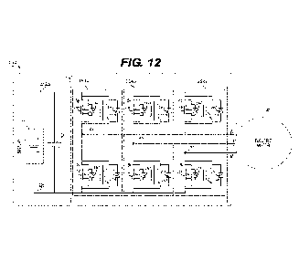
[0073] FIG. 12 is a schematic diagram of a fourth motor drive 150
according to an
aspect of the disclosure. Specifically, the fourth motor drive 150 includes a
fourth inverter
152, which may be similar in construction and operation to the first inverter
120 described
above with reference to FIG. 9. The fourth inverter 152 includes a phase
driver 154a, 154b,
154c, each configured to switch current from the DC source 70 to generate AC
power upon
corresponding ones of the output terminals 74, 78. Unlike the first inverter
120 described
above with reference to FIG. 9, the phase drivers 154a, 154b, 154c within the
fourth
inverter 152 each include two or more different solid-state switches, each
having a different
voltage rating. Each of the phase drivers 154a, 154b, 154c includes a high-
side switch Sh
and a low-side switch Si, with each of the switches Sh, Si including two
different solid-state
switches 156, 158, each having a different voltage rating. Each of the two
different solid-
state switches 156, 158 is shown with a corresponding body diode 160, 162, but
the
CA 03137719 2021-10-21
WO 2020/219857
PCT/US2020/029784
presence of the body diodes 160, 162 may depend on the type of devices used
for the two
different solid-state switches 156, 158. In the illustrated example, each of
the switches Sh, Si
includes a first solid-state switch 156 connected in parallel with a second
solid-state switch
158 such that current can flow between the DC source 22a, 22b and a
corresponding one of
the output terminals 30a, 30b, 30c with either of the first solid-state switch
156 or the
second solid-state switch 158 in a conductive state. In practice, the first
solid-state switch
156 and the second solid-state switch 158 are synchronized, thus splitting
current
approximately evenly therebetween.
[0074] The first solid-state switches 156 are Silicon carbide (SiC)
transistors and the
second solid-state switches 158 are insulated gate bipolar transistors (IGBT)
in the example
embodiment shown in FIG. 12. More specifically, the first solid-state switch
156 in an
example embodiment is a SiC transistor having part number SCT3017AL from Rohm
Semiconductor, and the second solid-state switch 158 is an IGBT having part
number
AUIRGPS4070D0 from Infineon. However, different types of solid-state switches
may be
used for either or both of the first solid-state switches 156 and/or the
second solid-state
switches 158. Also, the switches Sh, Si may have a different arrangement of
the different
solid-state switches 156, 158. For example, one or more of the high-side
switches Sh and/or
the low-side switches Si may comprise two of the first solid-state switches
156 connected in
series with one another, and one of the second solid-state switches 158
connected in parallel
with the series combination of the first solid-state switches 156. Such a
combination may be
capable of switching loads having a higher voltage than a single one of the
first solid-state
switches 156. The fourth inverter 152 may be called a "hybrid inverter" as a
result of
including the two or more different solid-state switches. Such a hybrid
inverter may provide
a significant improvement in inverter efficiency. However, a hybrid inverter
may present
26
CA 03137719 2021-10-21
WO 2020/219857
PCT/US2020/029784
challenges in synchronizing operation of the different solid-state switches
156, 158 in a
given one of the switches SI,' Si.
[0075] FIG. 13 is a schematic diagram 170 of solid-state switches 156,
158 with
gate driver circuits 172, 176 in accordance with some embodiments of the
present
disclosure. Each of the gate driver circuits 172, 176 functions as a delay
driver to regulate
flow of electrical current to and from a control terminal 174, 178 of a
corresponding one of
the solid-state switches 156, 158 in order to synchronize turn-on and turn-off
of the solid-
state switches 156, 158 based on a shared gate pulse control 180. The control
terminals 174,
178 are gate terminals for Field-Effect Transistor (FET) or IGBT type solid-
state switches
156, 158. However, the control terminal may be another structure for other
types of solid-
state switches 156, 158.
[0076] The first gate driver 172 is configured to energize a first
control terminal 174
of the first solid-state switch 156 to cause the first solid-state switch 156
to change between
a non-conductive state and a conductive state a first delay time after
assertion of the gate
pulse control 180. Specifically, the first gate driver 172 includes a first on-
control resistor
182 having a resistance value Ro_on connected in series with a first on-
control diode 183.
The series combination of the first on-control resistor 182 and the first on-
control diode 183
are connected between the gate pulse control 180 and the first control
terminal 174 of the
first solid-state switch 156 with a cathode of the on-control diode 183
connected directly to
the first control terminal 174 of the first solid-state switch 156. The
resistance value RgLon
of the first on-control resistor 182 controls the first delay time between
assertion of the gate
pulse control 180 and when the first solid-state switch 156 changes between
the non-
conductive state and the conductive state.
[0077] The first gate driver 172 is also configured to de-energize the
first control
terminal 174 of the first solid-state switch 156 to cause the first solid-
state switch 156 to
27
CA 03137719 2021-10-21
WO 2020/219857
PCT/US2020/029784
change between the conductive state and the non-conductive state a second
delay time after
de-assertion of the gate pulse control 180. Specifically, the first gate
driver 172 includes a
first off-control resistor 184 having a resistance value Ro_off connected in
series with a first
off-control diode 185. The series combination of the first off-control
resistor 184 and the
first off-control diode 185 are connected between the gate pulse control 180
and the first
control terminal 174 of the first solid-state switch 156 with an anode of the
off-control
diode 185 connected directly to the first control terminal 174 of the first
solid-state switch
156. The resistance value Rgl_off of the first off-control resistor 184
controls the second
delay time between de-assertion of the gate pulse control 180 and when the
first solid-state
switch 156 changes between the conductive state and the non-conductive state.
[0078] The second gate driver 176 is configured to energize a second
control
terminal 178 of the second solid-state switch 158 to cause the second solid-
state switch 158
to change between a non-conductive state and a conductive state a third delay
time after
assertion of the gate pulse control 180. Specifically, the second gate driver
176 includes a
second on-control resistor 182 having a resistance value Rg2 on connected in
series with a
second on-control diode 193. The series combination of the second on-control
resistor 192
and the second on-control diode 193 are connected between the gate pulse
control 180 and
the second control terminal 178 of the second solid-state switch 158 with a
cathode of the
on-control diode 193 connected directly to the second control terminal 178 of
the second
solid-state switch 158. The resistance value Rg
2 on of the second on-control resistor 192
controls the third delay time between assertion of the gate pulse control 180
and when the
second solid-state switch 158 changes between the non-conductive state and the
conductive
state.
[0079] The second gate driver 176 is also configured to de-energize the
second
control terminal 178 of the second solid-state switch 158 to cause the second
solid-state
28
CA 03137719 2021-10-21
WO 2020/219857
PCT/US2020/029784
switch 156 to change between the conductive state and the non-conductive state
a second
delay time after de-assertion of the gate pulse control 180. Specifically, the
second gate
driver 176 includes a second off-control resistor 194 having a resistance
value Rg2 off
connected in series with a second off-control diode 195. The series
combination of the
second off-control resistor 194 and the second off-control diode 195 are
connected between
the gate pulse control 180 and the second control terminal 178 of the second
solid-state
switch 158 with an anode of the off-control diode 195 connected directly to
the second
control terminal 178 of the second solid-state switch 158. The resistance
value Rg2 off of the
second off-control resistor 194 controls the fourth delay time between de-
assertion of the
gate pulse control 180 and when the second solid-state switch 158 changes
between the
conductive state and the non-conductive state.
[0080] The resistance value Rg Lon of the first on-control resistor 182
and the
resistance value Rg2 on of the second on-control resistor 192 are selected to
cause the third
delay time to be the same as the first delay time, thus providing for the
first solid-state
switch 156 and the second solid-state switch 158 to change between the non-
conductive
state and the conductive state at a same time after assertion of the gate
pulse control 180.
Similarly, the resistance value Ro_offof the first off-control resistor 184
and the resistance
value Rg2 off of the second on-control resistor 194 are selected to cause the
fourth delay time
to be the same as the second delay time, thus providing for the first solid-
state switch 156
and the second solid-state switch 158 to change between the conductive state
and the non-
conductive state at a same time after de-assertion of the gate pulse control
180. These same
delay times may be referred to as synchronization between the solid-state
switches 156,
158. In other words, the gate drivers 172, 176 are each configured to energize
and de-
energize a corresponding one of the control terminals 174, 176 at different
rates to
synchronize operation of the solid-state switches 156, 158. In some
embodiments, the
29
CA 03137719 2021-10-21
WO 2020/219857
PCT/US2020/029784
resistance values Rgi Rg2 on of the on-control resistors 182, 192, may be
different from
one another to compensate for differences in the operation of the
corresponding solid-state
switches 156, 158. In some embodiments, the resistance values Ro_ off Rg2 off
of the off-
control resistors 184, 194, may be different from one another to compensate
for differences
in the operation of the corresponding solid-state switches 156, 158.
[0081] The
operation of the gate drivers 172, 176 to control the solid-state switches
156, 158 is described in equations (1) through (6), below. Equation (7)
expands the
definition of a synchronization time Tsyn, to a more general case with N
number of solid-
state switches connected in parallel.
dvg (T ) d(vg(Ti)¨vdsice(TJ))
i = C ___________ +Cgd I gc
g gs ge dt dt (1)
di
Vg Vdslce(Ti) ¨ Rg(Tj)ig¨(Lg+Ls1)=g
dt (2)
AVG th(T
R (
g ,intT )= j j R (T )
g,ext j
tG (3)
V th(T )
ton = ¨ron ln(1 g )
V (T )
gate j
t ¨ ¨2 MO Vgth(T'))
off ¨ off
V )
gate j (4)
VonT
Tdead ¨ toff ¨ ton ¨ v s
v dc (5)
Von
Tsync Tdead + t on ¨ t off + ¨Ts
V
dc (6)
Tsync,1-N = + ton,' toff ,1 = ............. Tdead,2+ t0n,2 ¨toff, 2 = =
Tdead,N ton,N toff ,N (7)
n=1 n=2 n=N
Index:
Rg,na Internal gate resistance
Rg,ext External gate resistance
A VG,th Gate threshold difference between two devices
Ig Gate current
ton, toff Turn ¨ on and off delay
Ton, Toff Turn ¨ on and off time constant
Vgate Gate voltage during operation
CA 03137719 2021-10-21
WO 2020/219857
PCT/US2020/029784
Tdead Conventional deadtime
Tsync Synchronous time for two parallel devices
Ts Switching period
Junction temperature of the semiconductors
Cgs/ge Gate ¨ source or emitter parasitic capacitance
Cgd/gc Gate ¨ drain or collector parasitic capacitance
[0082] The internal gate resistances Rg,int are characteristics of the
physical solid-
state switches 156, 158, and the external gate resistances Rg,ext are
characteristics of the the
gate drivers 172, 176. A combination of the internal gate resistances Rg,int
and the external
gate resistances Rg,ext define the turn-on delay and turn-off delay of the
solid-state switches
156, 158 after corresponding rising and falling edges of the gate pulse
control 180. The
turn-on delay and turn-off delay must be within a minimum limit to avoid
overlap between
the high-side switch Sh and the corresponding low-side switch Si, which is
also called
deadtime or conventional deadtime Tdead. Here, a synchronization time Tsyn, is
provided,
where the addition of deadtime Tdend, turn-on time ton and turn-off time toff
for each of the
solid-state switches 156, 158 connected in parallel will be equal to each
other as shown in
equation (6), above.
[0083] A gate current between one of the gate drivers 172, 176 and a
corresponding
one of the control terminals 174, 178 depends on the conducting current and
gate voltages.
Also, the parasitic capacitance at the one of the control terminals 174, 178
has major
influence on the gate current deviation in equation (1). The gate voltage is
identified based
on the gate current calculated in equation (2). Following, considering an
external resistance
and gate threshold voltage difference between two devices, internal resistance
has been
determined in equation (3), which is used to calculate switching delay in
equation (4). A
regular deadtime model is shown in equation (5). Subsequently, the deadtime
model is
being modified in equations (6) and (7), where a new coefficient Tsyn, is
introduced. The
31
CA 03137719 2021-10-21
WO 2020/219857
PCT/US2020/029784
coefficient is mostly depending on the switching delay to set the lower
boundary and the
T dead is optimized to adjust the synchronous time.
[0084] FIG. 14 is a schematic diagram showing different switching states
200-216
of a three-phase inverter, and which each have a corresponding vector
identification (the
circled number 0-7). Specifically, each of the switching states defines a
position for each of
three switches Sa, Sb, Se to conduct current between a corresponding one of
the output
terminals a, b, c, and either the high-side conductor 22a or the low-side
conductor. The first
through sixth switching states 200-212 are called active voltage vectors 1, 2,
3, 4, 5, 6, and
the remaining two of the switching states 214, 216 are referred to as zero
voltage vectors 0,
7, because they each cause the voltages in all three of the output terminals
a, b, c, to be
equal, thereby causing no voltage difference between any of the output
terminals a, b, c.
[0085] The switching states 200-216, and associated control methods,
such as space
vector pulse-width modulation (SVPWM) or near state pulse-width modulation
(NSPWM),
may also be used with the nine-switch invertor, such as the ones shown in
FIGS. 10-11, for
example, by corresponding assertions and de-assertions of the gate control
signals 90a, 90b,
90c. For example, active voltage vector 2, shown as switching state 202 on
FIG. 12 may
correspond to assertion of the a-phase and b-phase gate control signals 90a,
90b, and de-
assertion of the c-phase gate control signal 90c.
[0086] FIG. 15 is a graph showing inverter output voltage space vectors,
based upon
a space vector representation of the voltages in an a, 13 plane, where the a,
13 components are
found by a Clark transform. The six active voltage vectors 1, 2, 3, 4, 5, and
6 define six
sectors I, II, III, IV, V, and VI, each defining a 60-degree range between two
adjacent ones
of the active voltage vectors 1, 2, 3, 4, 5, 6. In some embodiments, the
switching transistors
within the inverter 126, 126', 126" may be controlled using the SVPWM control
method to
generate an output voltage vector Veef within any of the sectors I, II, III,
IV, V, and VI, by
32
CA 03137719 2021-10-21
WO 2020/219857
PCT/US2020/029784
controlling the switching transistors in a sequence that uses the two active
voltage vectors 1,
2, 3, 4, 5, and 6 that define the boundary of the one of the sectors I, II,
III, IV, V, VI, that
contains output voltage vector Võf, in addition to one or more of the zero
voltage vectors 0,
7. For example, and with reference to FIG. 15 the example output voltage
vector Vref within
the first sector I may be produced on the output terminals a, b, c, by
switching the switches
Sa, Sb, Se of the three-phase inverter in a pattern using the first and second
active voltage
vectors 1, 2, and the two zero voltage vectors 0, 7. In some embodiments, each
change in
switching state may include changing the state of only one of the three
switches Sa, Sb, Sc.
Thus, the SVPWM algorithm may use both of the zero voltage vectors 0, 7. The
time spent
at each of the zero voltage vectors 0, 7 may be evenly divided before and
after the time
spent at each of two of the active voltage vectors 1, 2, 3, 4, 5, 6. For
example, the SVPWM
algorithm may use a 0,1,2,7 - 7,2,1,0 sequence in the first sector I. This
sequence extends
for two sampling time intervals, with the second sampling time interval having
a switching
pattern that is the reverse order of the switching pattern in the first
sampling time interval.
Each of the two sampling time intervals, thus includes four different
switching states 214,
200, 202, 216 to produce the two active voltage vectors 1, 2, and the two zero
voltage
vectors 0, 7. Three different changes of the switching states 214, 200, 202,
216, or
commutations, are used within each sampling time interval to define each
sequence in the
SVPWM algorithm.
[0087] FIG. 16 is a graph showing inverter output voltage vectors with
near-state
control sectors I', II', III', IV', V', VI', which are each defined by and
centered-around a
corresponding one of the active voltage vectors 1, 2, 3, 4, 5, 6. In some
embodiments, each
of the phase drivers 134a, 134b, 134c, 144a, 144b, 144c is controlled to
generate an output
voltage vector upon a corresponding one of the one or more output terminals
74, 78 using
the NSPWM control method, which may also be called an NSPWM algorithm.
Specifically,
33
CA 03137719 2021-10-21
WO 2020/219857
PCT/US2020/029784
the NSPWM control method may include switching the one or more output
terminals 74, 78
between a nearest-one of the active voltage vectors 1, 2, 3, 4, 5, 6 having an
angle closest to
the output voltage vector Võf, (i.e. the one of the active voltage vectors 1,
2, 3, 4, 5, 6
associated with the one of the control sectors I', II', III', IV', V', VI'
where the output
voltage vector Võfis located), and two neighboring active voltage vectors on
either angular
side of the nearest-one of the active voltage vectors 1, 2, 3, 4, 5, 6. For
example, the
NSPWM algorithm may use a 2,1,6 ¨ 6,1,2 sequence in the first control sector
I'. Two
different changes of the switching states 202, 200, 212, or commutations, are
made within
each sampling time interval to define each sequence in the NSPWM algorithm.
Also, the
NSPWM algorithm includes switching the one or more output terminals 74, 78
only to
active voltage vectors 1, 2, 3, 4, 5, 6 and not to either of the zero voltage
vectors 0, 7 in
order to generate the output voltage vector Võfhaving a non-zero scalar value.
[0088] The
present disclosure provides a motor drive for providing AC power to an
electric motor, the motor drive comprising: a battery bus for connection to a
battery and
defining a positive source node and a reference source node and configured to
provide DC
electrical power having a substantially constant voltage; a voltage-to-current
(V-I) converter
operable in a traction mode to receive the first DC electrical power from the
battery bus and
to supply DC electrical power having a substantially constant current upon a
DC link bus; a
current-source inverter (CSI) including a plurality of solid-state switches
configured to
generate an AC power upon one or more motor leads by selectively switching the
second
DC electrical power from the V-I converter; wherein the V-I converter is
operable in a
charging mode to receive power from the DC link bus and to supply power to the
battery
bus; and wherein each of the solid-state switches in the current-source
inverter are wide-
bandgap (WBG) devices having a bandgap greater than 2.0 electron-volts (eV).
34
CA 03137719 2021-10-21
WO 2020/219857
PCT/US2020/029784
[0089] In some
embodiments, the motor drive of the preceding section may further
comprise: wherein each of the solid-state switches in the current-source
inverter has a
bandgap of between 2 and 4 electron-volts (eV).
[0090] In some
embodiments, the motor drive of any of the preceding sections may
further comprise: wherein each of the solid-state switches in the current-
source inverter are
Silicon carbide (SiC) transistors.
[0091] In some
embodiments, the motor drive of any of the preceding sections may
further comprise: wherein each of the solid-state switches in the current-
source inverter are
Gallium nitride (GaN) transistors.
[0092] In some
embodiments, the motor drive of any of the preceding sections may
further comprise: wherein the V-I converter is configured to boost a first DC
voltage from
the DC link bus to a second DC voltage upon the battery bus in the charging
mode, with the
second DC voltage greater than the first DC voltage.
[0093] In some
embodiments, the motor drive of any of the preceding sections may
further comprise: wherein the second DC voltage is at least two-times the
first DC voltage.
[0094] In some
embodiments, the motor drive of any of the preceding sections may
further comprise: wherein the V-I converter includes a quasi-Z-Source (qZS).
[0095] In some
embodiments, the motor drive of any of the preceding sections may
further comprise: wherein the quasi-Z-Source (qZS) comprises: a DC Bus
inductor defining
a first lead and a second lead, with the first lead connected to the positive
source node of the
battery bus; a first winding defining a first lead and a second lead; a second
winding
defining a first lead and a second lead; a first capacitor defining a first
terminal and a
second terminal; and a rectifier defining an input terminal and an output
terminal.
[0096] In some
embodiments, the motor drive of any of the preceding sections may
further comprise: a second capacitor defining a first terminal and a second
terminal;
CA 03137719 2021-10-21
WO 2020/219857
PCT/US2020/029784
wherein the first winding and the second winding are each inductors; and
wherein the quasi-
Z-Source inverter (qZSI) includes: the reference source node of the battery
bus connected to
a low-side conductor of the DC link bus; the second lead of the DC bus
inductor connected
to a high-side conductor of the DC link bus and to the first lead of the first
winding; the
second lead of the first winding defining a first internal node; the first
terminal of the first
capacitor connected to the first internal node, and the second terminal of the
first capacitor
connected to the low-side conductor of the DC link bus; the output terminal of
the rectifier
connected to the first internal node, and the input terminal of the rectifier
defining a second
internal node; the first terminal of the second capacitor connected to the
high-side conductor
of the DC link bus, and the second terminal of the second capacitor connected
to the second
internal node; the first lead of the second winding connected to the second
internal node,
and the second lead of the second winding connected to the low-side conductor
of the DC
link bus.
[0097] In some
embodiments, the motor drive of any of the preceding sections may
further comprise: a second capacitor defining a first terminal and a second
terminal;
wherein the first winding and the second winding are each inductors; and
wherein the quasi-
Z-Source inverter (qZSI) includes: the second lead of the DC bus inductor
defining a first
internal node; the first lead of the first winding connected to the first
internal node, and the
second lead of the fist inductor connected to a high-side conductor of the DC
link bus; the
first terminal of the first capacitor connected to the first internal node,
and the second
terminal of the first capacitor connected to the low-side conductor of the DC
link bus; the
output terminal of the rectifier connected to the first internal node, and the
input terminal of
the rectifier connected to the reference source node of the battery bus; the
first terminal of
the second capacitor connected to the high-side conductor of the DC link bus,
and the
second terminal of the second capacitor connected to the reference source node
of the
36
CA 03137719 2021-10-21
WO 2020/219857
PCT/US2020/029784
battery bus; the first lead of the second winding connected to the reference
source node of
the battery bus, and the second lead of the second winding connected to the
low-side
conductor of the DC link bus.
[0098] In some
embodiments, the motor drive of any of the preceding sections may
further comprise: wherein the first winding and the second winding are
magnetically
coupled as a transformer having a n:1 turns ratio, where n is an integer
number; and wherein
the quasi-Z-Source inverter (qZSI) includes: the reference source node of the
battery bus
connected to a low-side conductor of the DC link bus; the second lead of the
DC bus
inductor connected to a high-side conductor of the DC link bus and to the
first lead of the
first winding; the second lead of the first winding defining a first internal
node; the first
terminal of the first capacitor connected to the first internal node, and the
second terminal of
the first capacitor connected to the low-side conductor of the DC link bus;
the first lead of
the second winding connected to the first internal node, and the second lead
of the second
winding defining a second internal node; the output terminal of the rectifier
connected to the
second internal node, and the input terminal of the rectifier connected to the
low-side
conductor of the DC link bus.
[0099] In some
embodiments, the motor drive of any of the preceding sections may
further comprise: wherein the first winding and the second winding are
magnetically
coupled as a transformer having a 1:n turns ratio, where n is an integer
number; and wherein
the quasi-Z-Source inverter (qZSI) includes: the reference source node of the
battery bus
connected to a low-side conductor of the DC link bus; the second lead of the
DC bus
inductor defining a first internal node; the first lead of the first winding
connected to the
first internal node, and the second lead of the first winding defining a
second internal node;
the first lead of the second winding connected to the second internal node,
and the second
lead of the second winding connected to a high-side conductor of the DC link
bus; the
37
CA 03137719 2021-10-21
WO 2020/219857
PCT/US2020/029784
output terminal of the rectifier connected to the first internal node, and the
input terminal of
the rectifier connected to the low-side conductor of the DC link bus; and the
first terminal of
the first capacitor connected to the second internal node, and the second
terminal of the first
capacitor connected to the low-side conductor of the DC link bus.
[0100] In some
embodiments, the motor drive of any of the preceding sections may
further comprise: wherein the rectifier includes a diode, and wherein the
input terminal is an
anode of the diode and the output terminal is a cathode of the diode.
[0101] In some
embodiments, the motor drive of any of the preceding sections may
further comprise: wherein the rectifier includes a bidirectionally conducting,
unidirectionally blocking switch.
[0102] The
present disclosure also provides motor drive for providing AC power to
an electric motor, the motor drive comprising: a direct current (DC) voltage
source
configured to provide a first DC electrical power having a substantially
constant voltage; a
DC link bus including a high-side conductor and a low-side conductor; a nine-
switch
inverter coupled to the DC link bus and including nine solid-state switches
configured to
generate 3-phase AC power upon a first set of motor leads to supply a first
winding set
within the electric motor, the nine solid-state switches in the inverter also
configured to
generate 3-phase AC power upon a second set of motor leads to supply a second
winding
set within the electric motor; wherein the nine-switch inverter includes: an a-
phase high
switch configured to selectively conduct current between the high-side
conductor and a first
motor lead of the first set of motor leads; a b-phase high switch configured
to selectively
conduct current between the high-side conductor and a second motor lead of the
first set of
motor leads; a c-phase high switch configured to selectively conduct current
between the
high-side conductor and a third motor lead of the first set of motor leads; an
a-phase low
switch configured to selectively conduct current between the low-side
conductor and a first
38
CA 03137719 2021-10-21
WO 2020/219857
PCT/US2020/029784
motor lead of the second set of motor leads; a b-phase low switch configured
to selectively
conduct current between the low-side conductor and a second motor lead of the
second set
of motor leads; a c-phase low switch configured to selectively conduct current
between the
low-side conductor and a third motor lead of the second set of motor leads; an
a-phase
middle switch configured to selectively conduct current between the first
motor lead of the
first set of motor leads and the first motor lead of the second set of motor
leads; a b-phase
middle switch configured to selectively conduct current between the second
motor lead of
the first set of motor leads and the second motor lead of the second set of
motor leads; and a
c-phase middle switch configured to selectively conduct current between the
third motor
lead of the first set of motor leads and the third motor lead of the second
set of motor leads;
and wherein the nine-switch inverter is configured to be operated in a
rectifier mode to
convert the 3-phase AC electrical current from each of the first and second
sets of motor
leads to supply DC power to the DC voltage source via the DC link bus.
[0103] In some embodiments, the motor drive the preceding section may
further
comprise: wherein each of the solid-state switches in the nine-switch inverter
are wide-
bandgap (WBG) devices having a bandgap greater than 2.0 electron-volts (eV).
[0104] In some embodiments, the motor drive of any of the preceding
sections may
further comprise: wherein each of the solid-state switches in the nine-switch
inverter are
Silicon carbide (SiC) transistors.
[0105] In some embodiments, the motor drive of any of the preceding
sections may
further comprise: wherein each of the solid-state switches in the nine-switch
inverter are
Gallium nitride (GaN) transistors.
[0106] In some embodiments, the motor drive of any of the preceding
sections may
further comprise: wherein the nine-switch inverter is configured to supply the
3-phase AC
39
CA 03137719 2021-10-21
WO 2020/219857
PCT/US2020/029784
power upon the second set of motor leads having a phase difference of 180
degrees from the
3-phase AC power upon the first set of motor leads.
[0107] In some embodiments, the motor drive of any of the preceding
sections may
further comprise: wherein the nine-switch inverter is configured to supply the
3-phase AC
power upon the second set of motor leads having an opposite polarity to the
first set of
motor leads.
[0108] A motor drive system for an electrified vehicle includes a
battery bus for
connection to a battery and a voltage-to-current (V-I) converter, operable to
transfer power
from the battery bus to an electric motor or in a charging mode to supply
power to the
battery bus. A current-source inverter (CSI) includes a plurality of wide-
bandgap (WBG)
switches, such as Silicon carbide (SiC) or Gallium nitride (GaN) devices
configured to
generate an AC power upon one or more motor leads by selectively switching DC
electrical
power from a DC link bus connected to the V-I converter. The V-I converter may
include a
quasi-Z-Source (qZS) and may boost a first DC voltage from the DC link bus to
a larger DC
voltage upon the battery bus. A motor drive including a nine-switch inverter
(NSI) with
WBG switches may be operated in either an inverter mode or a rectifier mode.
[0109] The foregoing description of the embodiments has been provided for
purposes of
illustration and description. It is not intended to be exhaustive or to limit
the disclosure.
Individual elements or features of a particular embodiment are generally not
limited to that
particular embodiment, but, where applicable, are interchangeable and can be
used in a
selected embodiment, even if not specifically shown or described. The same may
also be
varied in many ways. Such variations are not to be regarded as a departure
from the
disclosure, and all such modifications are intended to be included within the
scope of the
disclosure.