Note: Descriptions are shown in the official language in which they were submitted.
CA 03138526 2021-10-28
WO 2020/223697
PCT/US2020/031168
MICROFABRICATED DEVICE WITH HYDROPHILIC MICRO WELLS
30 AND HYDROPHOBIC INTERSTITIAL SPACE
Cross Reference to Related Application
This application claims the benefit of priority of U.S. Provisional Patent
Application No.
62/842,456, filed May 2, 2019, the disclosure of which is incorporated by
reference herein in its
35 entirety.
Background
Microfluidic devices have been exploited in the drug discovery industry and
for
improving experimentation in a variety of areas in biology, such as cell
culture. Advantages of
40 micro analysis systems include reduced sample size, precise micro
environmental control, and
parallel operation in a single device yielding the ability to perform high
throughput analyses.
Due to the microscale size of the fluid channels and reaction chambers on
microfluidic
devices, complex peripheral equipment is often required to manipulate the
fluid flow on such devices.
Capillary microfluidics can deliver liquids in a pre-programmed manner without
peripheral equipment
45 by exploiting capillary effects rendered by the surface chemistry of
microchannels. However,
precision lithography and channel surface treatment may be needed.
With platforms comprising a high-density array of microwells and with no
microchannel
interconnections, loading the array of wells and keeping the contents of the
wells isolated from
each other can be a challenge. In particular, if the platform is fabricated by
a hydrophobic
50 material, such as a hydrophobic plastic, loading aqueous solutions into
the array of microwells
may be impeded by surface tension and trapped air in the microwells.
Summary of the Invention
In one aspect, the present disclosure provides a method of modifying a
microfabricated
55 chip having a top surface including a plurality of microwells each
having a bottom and a side
wall, and interstitial space between the microwells, the microfabricated chip
being made of a
hydrophobic material. The method comprises, in the following order: (a)
treating the
microfabricated chip to render the surface of the bottom and side wall of the
microwells and the
interstitial space hydrophilic; and (b) selectively treating the surface of
the interstitial space to
1
CA 03138526 2021-10-28
WO 2020/223697
PCT/US2020/031168
render it hydrophobic.
In some embodiments of the method, step (a) comprises treating the
microfabricated chip
with plasma. In some embodiments of the method, step (a) comprises treating
the
microfabricated chip with one of corona discharge, ozone, and copper-enhanced
oxidation.
In some embodiments of the method, step (a) comprises forming a hydrophilic
layer of
small molecule or polymer, e.g., by photochemical surface modification, on the
surface of the
bottom and side wall of the microwells and the interstitial space of the
microfabricated chip.
In some embodiments of the method, step (b) comprises contacting an object
with the
surface of the interstitial space so as to impart hydrophobicity to the
surface of the interstitial
space.
In some embodiments, step (b) comprises selectively removing a top layer of
the surface
of the interstitial space.
In some embodiments, before step (b), the method further includes: (c)
applying a
hydrophilic liquid on the microfabricated device to fill at least a portion of
each of the plurality
of wells with the liquid. Such application of the hydrophilic liquid can cause
a portion of the
liquid to be retained on the interstitial space. In some of these embodiments,
the method further
comprises: after (c) and before (b): (d) removing the portion of liquid
retained on the interstitial
space. Removal of the restrained liquid can be accomplished by controlled
evaporation, or by
using a soft blade to swipe through the interstitial space surface, or by
using an absorbent
.. material to remove the retained liquid on the interstitial space by
absorption.
In some embodiments, step (b) comprises spraying an organic solvent onto the
surface of
the interstitial space. In other embodiments, step (b) comprises forming a
hydrophobic polymer
layer on the surface of the interstitial space.
In another aspect, the present disclosure provides a method of modifying a
microfabricated chip having a top surface including a plurality of microwells
each having an
interior surface and an interstitial space between the microwells, the
microfabricated chip being
made of a hydrophobic material. The method comprises, in the following order:
(a) applying a
hydrophilic liquid on the microfabricated chip so as to fill at least a
portion of each of the
plurality of wells with the hydrophilic liquid; (b) if any portion of the
hydrophilic liquid remains
.. on the interstitial space, removing the portion of the hydrophilic liquid
from the interstitial space;
and (c) converting the interior surface of the microwells to hydrophilic. The
hydrophilic liquid
2
CA 03138526 2021-10-28
WO 2020/223697
PCT/US2020/031168
can be an aqueous solution containing a water soluble polymer, such as
poly(vinyl alcohol)
(PVA).
In a further aspect, the present disclosure provides a microfabricated device
having a top
surface defining an array of microwells having a surface density of at least
750 microwells per
.. cm2 , each microwell having a bottom and a side wall, and interstitial
space between the
microwells, the microfabricated device being made of a hydrophobic base
material, where the
internal surfaces of the microwells are modified to be hydrophilic and the
interstitial space
between the microwells is hydrophobic.
In a further aspect, the present disclosure provides a method of culturing and
screening
.. for at least one biological entity of interest using a microfabricated
device having a top surface
defining an array of microwells having a surface density of at least 750
microwells per cm2,
wherein each of the microwells has a bottom and a side wall and an
interstitial space between the
microwells, the microfabricated device being made of a hydrophobic material
where the internal
surfaces of the microwells are hydrophilic and the interstitial space between
the microwells is
hydrophobic. The method includes: loading a sample onto the microfabricated
device such that at
least one microwell of the array of microwells includes at least one cell and
an amount of a
nutrient; applying a membrane to the microfabricated device to retain the at
least one cell and the
nutrient in the at least one microwell of the array of microwells; without
furnishing additional
nutrient, culturing a plurality of cells from the at least one cell in the at
least one microwell of the
array of microwells; and analyzing the plurality of cells to determine a
presence or absence of a
biological entity of interest.
Brief Description of the Drawings
The skilled artisan will understand that the drawings primarily are for
illustrative
purposes and are not intended to limit the scope of the inventive subject
matter described herein.
The drawings are not necessarily to scale; in some instances, various aspects
of the inventive
subject matter disclosed herein may be shown exaggerated or enlarged in the
drawings to
facilitate an understanding of different features. In the drawings, like
reference characters
generally refer to like features (e.g., functionally similar and/or
structurally similar elements).
FIG. 1 is a perspective view illustrating a microfabricated device or chip in
accordance
with some embodiments.
3
CA 03138526 2021-10-28
WO 2020/223697
PCT/US2020/031168
FIGS. 2A-2C are top, side, and end views, respectively, illustrating
dimensions of
microfabricated device or chip in accordance with some embodiments.
FIGS. 3A and 3B are exploded and top views, respectively, illustrating a
microfabricated
device or chip in accordance with some embodiments.
FIG. 4 is a schematic depiction of a cross section of a microfabricated device
in
accordance with some embodiments, the microfabricated device including
microwells where the
internal surfaces of the microwells are hydrophilic and the interstitial space
between the
microwells is hydrophobic.
Detailed Description of Embodiments of the Invention
An object of the present invention is to provide a microfabricated device (or
chip) having
a top surface defining an array of microwells and interstitial space between
the microwells, the
microfabricated device being made of a hydrophobic polymer material, where the
internal
surfaces of the microwells are hydrophilic and the interstitial space between
the microwells is
hydrophobic. The microwells each have a bottom and a side wall. The term
"bottom" is used
herein to indicate that the microwells have finite depth in the thickness
direction of the
microfabricated device and are not through holes across the microfabricated
device. The bottom
and the side wall may have clear boundaries between them, but can also be
smoothly joined
without obvious demarcation. Another object of the present invention is to
provide methods to
modify a microfabricated chip made of a hydrophobic material such that the
internal surfaces of
the microwells becomes hydrophilic and the interstitial space between the
microwells remains
hydrophobic. These characteristics would significantly simplify the loading,
sealing, cell
retention in the microwells, as well as downstream operations such as picking
and transferring
samples from microwells.
In some embodiments, the high density cell cultivation platform can be a
microfabricated
device (or a "chip"). As used herein, a microfabricated device or chip may
define a high density
array of microwells (or experimental units). For example, a microfabricated
chip comprising a
"high density" of microwells may include about 150 microwells per cm2 to about
160,000
microwells or more per cm2 (for example, at least 150 microwells per cm2, at
least 250
microwells per cm2, at least 400 microwells per cm2, at least 500 microwells
per cm2, at least 750
4
CA 03138526 2021-10-28
WO 2020/223697
PCT/US2020/031168
microwells per cm2, at least 1,000 microwells per cm2, at least 2,500
microwells per cm2, at least
5,000 microwells per cm2, at least 7,500 microwells per cm2, at least 10,000
microwells per cm2,
at least 50,000 microwells per cm2, at least 100,000 microwells per cm2, or at
least 160,000
microwells per cm2). A substrate of a microfabricated chip may include about
or more than
10,000,000 microwells or locations. For example, an array of microwells may
include at least 96
locations, at least 1.000 locations, at least 5,000 locations, at least 10,000
locations, at least
50,000 locations, at least 100,000 locations, at least 500,000 locations, at
least 1,000,000
locations, at least 5.000,000 locations, or at least 10,000,000 locations. The
arrays of microwells
may form grid patterns, and be grouped into separate areas or sections. The
dimensions of a
microwell may range from nanoscopic (e.g., a diameter from about 1 to about
100 nanometers)
to microscopic. For example, each microwell may have a diameter of about 1 gm
to about
800 gm, a diameter of about 25 tm to about 500 gm, or a diameter of about 30
gm to about
100 gm. A microwell may have a diameter of about or less than 1 gm, about or
less than 5 gm,
about or less than 10 .1m, about or less than 25 gm, about or less than 50 gm,
about or less than
100 gm, about or less than 200 gm, about or less than 300 gm, about or less
than 400 gm, about
or less than 500 gm, about or less than 600 gm, about or less than 700 gm, or
about or less than
800 gm. In exemplary embodiments, the diameter of the microwells can be about
100 gm or
smaller, or 50 gm or smaller. A microwell may have a depth of about 25 gm to
about 100 gm,
e.g., about 1 gm, about 5 gm, about 10 gm, about 25 gm, about 50 gm, about 100
gm. It can
also have greater depth, e.g., about 200 gm, about 300 gm, about 400 gm, about
500 gm. The
spacing between adjacent microwells can range from about 25 gm to about 500
gm, or about
gm to about 100 gm.
The microfabricated chip can have two major surfaces: a top surface and a
bottom
surface, where the microwells have openings at the top surface. Each microwell
of the
25 microwells may have an opening or cross section having any shape, e.g.,
round, hexagonal,
square, or other shapes. Each microwell may include sidewalls. For microwells
that are not
round in their openings or cross sections, the diameter of the microwells
described herein refer to
the effective diameter of a circular shape having an equivalent area. For
example, for a square
shaped microwell having side lengths of 10x10 microns, a circle having an
equivalent area (100
30 square microns) has a diameter of 11.3 microns. Each microwell may
include a sidewall or
sidewalls. The sidewalls may have a cross-sectional profile that is straight,
oblique, and/or
5
CA 03138526 2021-10-28
WO 2020/223697
PCT/US2020/031168
curved. Each microwell includes a bottom which can be flat, round, or of other
shapes. The
microfabricated chip (with the microwells thereon) may be manufactured from a
polymer, e.g., a
cyclic olefin polymer, via precision injection molding or some other process
such as embossing.
Other material of construction is also available, such as silicon and glass.
The chip may have a
substantially planar major surface. FIG. 1 shows a schematic depiction of a
microfabricated
chip, whose edges are generally parallel to the directions of the rows and the
columns of the
microwells on the chip.
The high density microwells on the microfabricated chip can be used for
receiving a
sample comprising at least one biological entity (e.g., at least one cell).
The term "biological
entity" may include, but is not limited to, an organism, a cell, a cell
component, a cell product,
and a virus, and the term "species" may be used to describe a unit of
classification, including, but
not limited to, an operational taxonomic unit (OTU), a genotype, a phylotype,
a phenotype, an
ecotype, a history, a behavior or interaction, a product, a variant, and an
evolutionarily
significant unit. The high density microwells on the microfabricated chip can
be used to conduct
various experiments, such as growth or cultivation or screening of various
species of bacteria and
other microorganisms (or microbes) such as aerobic, anaerobic, and/or
facultative aerobic
microorganisms. The microwells may be used to conduct experiments with
eukaryotic cells such
as mammalian cells. Also, the microwells can be used to conduct various
genomic or proteomic
experiments, and may contain cell products or components, or other chemical or
biological
substances or entities, such as a cell surface (e.g., a cell membrane or
wall), a metabolite, a
vitamin, a hormone, a neurotransmitter, an antibody, an amino acid, an enzyme,
a protein, a
saccharide, ATP, a lipid, a nucleoside, a nucleotide, a nucleic acid (e.g.,
DNA or RNA), a
chemical, e.g., a dye, enzyme substrate, etc.
In some embodiments, the high density cell cultivation platform can be droplet
based,
e.g., instead of array(s) of wells as experimental units on a microfabricated
chip, a population of
discrete droplets can be used to retain cells, media and other components for
cell cultivation.
Droplet generation methods, especially when combined with cell-sorter-on-a-
chip type
instrumentation, may be used to grow and screen microbes from a complex
environmental
sample. Droplets may be produced at several hundred Hz, meaning millions of
drops can be
produced in a few hours. A simple chip-based device may be used to generate
droplets and the
droplets may be engineered to contain a single cell. A system for generating
droplets containing
6
CA 03138526 2021-10-28
WO 2020/223697
PCT/US2020/031168
cell suspensions may contain one or small numbers of cells. The droplets can
be emulsions,
double emulsion, hydrogel, bubbles and complex particles, etc. For example,
aqueous drops may
be suspended in a nonmiscible liquid keeping them apart from each other and
from touching or
contaminating any surfaces. The volume of a droplet can be somewhere between
10 fl and
and highly monodisperse droplets can be made from a few nanometers up to 500
p.m in diameter.
A droplet-based microfluidic system may be used to generate, manipulate,
and/or incubate small
droplets. Cell survival and proliferation can be similar to control
experiments in bulk solution.
Fluorescence screening of droplets may be done on-chip and at a rate of, for
example, 500 drops
per second. Droplets may be merged to create a new droplet or a reagent added
to a droplet.
Droplets can be passed in a microchannel in a single file and interrogated by
a spectroscopic
method, e.g., using a fluorescence detector to detect fluorescence emitted
from the droplets, and
those droplets that are determined to meet certain criteria (e.g., emitting
fluorescence at certain
wavelength) can be selected via diversion into a branched channel from which
the droplet can be
pooled or harvested. The diversion or switching of flow can be accomplished by
valves, pump,
applying an external electric field, etc.
In various embodiments, a cell may be Archaea, Bacteria. or Eukaryota (e.g.,
fungi). For
example, a cell may be a microorganism, such as an aerobic, anaerobic, or
facultative aerobic
microorganisms. A virus may be a bacteriophage. Other cell components/products
may include,
but are not limited to, proteins, amino acids, enzymes, saccharides, adenosine
triphosphate
(ATP), lipids, nucleic acids (e.g., DNA and RNA). nucleosides, nucleotides,
cell
membranes/walls, flagella, fimbriae, organelles, metabolites, vitamins,
hormones,
neurotransmitters, and antibodies.
For the cultivation of cells, a nutrient is often provided. A nutrient may be
defined (e.g., a
chemically defined or synthetic medium) or undefined (e.g., a basal or complex
medium). A
nutrient may include or be a component of a laboratory-formulated and/or a
commercially
manufactured medium (e.g., a mix of two or more chemicals). A nutrient may
include or be a
component of a liquid nutrient medium (i.e., a nutrient broth), such as a
marine broth, a lysogeny
broth (e.g., Luria broth), etc. A nutrient may include or be a component of a
liquid medium
mixed with agar to form a solid medium and/or a commercially available
manufactured agar
plate, such as blood agar.
A nutrient may include or be a component of selective media. For example,
selective
7
CA 03138526 2021-10-28
WO 2020/223697
PCT/US2020/031168
media may be used for the growth of only certain biological entities or only
biological entities
with certain properties (e.g., antibiotic resistance or synthesis of a certain
metabolite). A nutrient
may include or be a component of differential media to distinguish one type of
biological entity
from another type of biological entity or other types of biological entities
by using biochemical
characteristics in the presence of specific indicator (e.g., neutral red,
phenol red, eosin y, or
methylene blue).
A nutrient may include or be a component of an extract of or media derived
from a
natural environment. For example, a nutrient may be derived from an
environment natural to a
particular type of biological entity, a different environment, or a plurality
of environments. The
environment may include, but is not limited to, one or more of a biological
tissue (e.g.,
connective, muscle, nervous, epithelial, plant epidermis, vascular, ground,
etc.), a biological fluid
or other biological product (e.g., amniotic fluid, bile, blood, cerebrospinal
fluid, cerumen,
exudate, fecal matter, gastric fluid, interstitial fluid, intracellular fluid,
lymphatic fluid, milk,
mucus, rumen content, saliva, sebum, semen, sweat, urine, vaginal secretion,
vomit, etc.), a
microbial suspension, air (including, e.g., different gas contents),
supercritical carbon dioxide,
soil (including, e.g., minerals, organic matter, gases, liquids, organisms,
etc.), sediment (e.g.,
agricultural, marine, etc.), living organic matter (e.g., plants, insects,
other small organisms and
microorganisms), dead organic matter, forage (e.g., grasses, legumes, silage,
crop residue, etc.), a
mineral, oil or oil products (e.g., animal, vegetable, petrochemical), water
(e.g., naturally-
sourced freshwater, drinking water, seawater, etc.), and/or sewage (e.g.,
sanitary, commercial,
industrial, and/or agricultural wastewater and surface runoff).
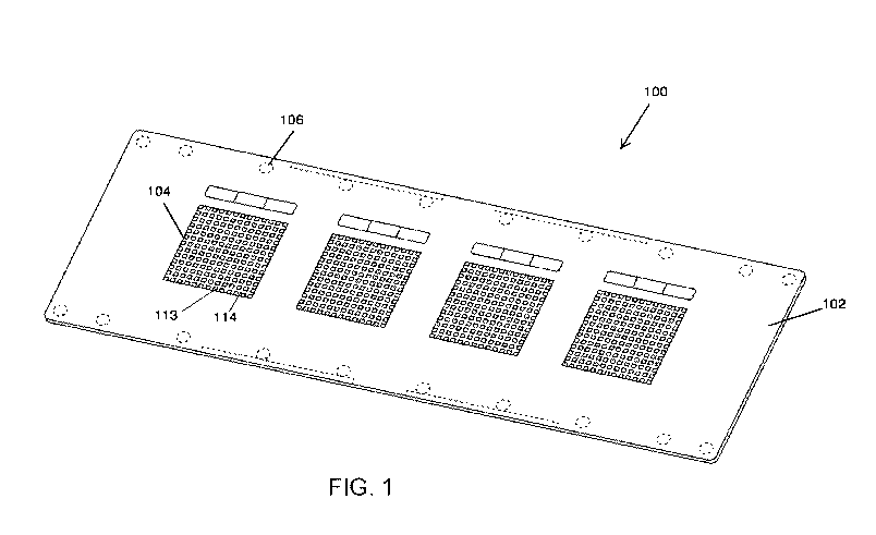
FIG. 1 is a perspective view illustrating a microfabricated device or chip in
accordance
with some embodiments. Chip 100 includes a substrate shaped in a microscope
slide format with
injection-molded features on top surface 102. The features include four
separate microwell
arrays (or microarrays) 104 as well as ejector marks 106. The microwells 113
(spaced by
interstitial space 114) in each microarray are arranged in a grid pattern with
well-free margins
around the edges of chip 100 and between microarrays 104. FIG. 4 shows a
schematic cross
section view of a portion of a microfabricated device or chip of the present
disclosure, where the
internal surfaces (side wall and bottom) of the microwells 113 are hydrophilic
and the interstitial
space 114 between the microwells is hydrophobic.
FIGS. 2A-2C are top, side, and end views, respectively, illustrating
dimensions of chip
8
CA 03138526 2021-10-28
WO 2020/223697
PCT/US2020/031168
100 in accordance with some embodiments. In FIG. 2A, the top of chip 100 is
approximately
25.5 mm by 75.5 mm. In FIG. 2B, the end of chip 100 is approximately 25.5 mm
by 0.8 mm. In
FIG. 2C, the side of chip 100 is approximately 75.5 mm by 0.8 mm.
After a sample is loaded on a microfabricated device, a membrane may be
applied to at
least a portion of a microfabricated device. FIG. 3A is an exploded diagram of
the
microfabricated device 300 shown from a top view in FIG. 3B in accordance with
some
embodiments. Device 300 includes a chip with an array of wells 302 holding,
for example, soil
microbes. A membrane 304 is placed on top of the array of wells 302. A gasket
306 is placed
on top of the membrane 304. A cover 308 with fill holes 310 is placed on top
of the gasket 306.
Finally, sealing tape 312 is applied to the cover 308.
A membrane may cover at least a portion of a microfabricated device including
one or
more experimental units or microwells. For example, after a sample is loaded
on a
microfabricated device, at least one membrane may be applied to at least one
microwell of a high
density array of microwells. A plurality of membranes may be applied to a
plurality of portions
of a microfabricated device. For example, separate membranes may be applied to
separate
subsections of a high density array of microwells.
A membrane may be connected, attached, partially attached, affixed, sealed,
and/or
partially sealed to a microfabricated device to retain at least one biological
entity in the at least
one microwell of the high density array of microwells. For example, a membrane
may be
reversibly affixed to a microfabricated device using lamination. A membrane
may be punctured,
peeled back, detached, partially detached, removed, and/or partially removed
to access at least
one biological entity in the at least one microwell of the high density array
of microwells.
A portion of the population of cells in at least one experimental unit, well,
or microwell
may attach to a membrane (via, e.g., adsorption). If so, the population of
cells in at least one
experimental unit, well, or microwell may be sampled by peeling back the
membrane such that
the portion of the population of cells in the at least one experimental unit,
well, or microwell
remains attached to the membrane.
A membrane may be impermeable, semi-permeable, selectively permeable,
differentially
permeable, and/or partially permeable to allow diffusion of at least one
nutrient into the at least
one microwell of a high density array of microwells. For example, a membrane
may include a
natural material and/or a synthetic material. A membrane may include a
hydrogel layer and/or
9
CA 03138526 2021-10-28
WO 2020/223697
PCT/US2020/031168
filter paper. In some embodiments, a membrane is selected with a pore size
small enough to
retain at least some or all of the cells in a microwell. For mammalian cells,
the pore size may be
a few microns and still retain the cells. However, in some embodiments, the
pore size may be
less than or equal to about 0.2 pm, such as 0.1 p.m. An impermeable membrane
has a pore size
.. approaching zero. It is understood that the membrane may have a complex
structure that may or
may not have defined pore sizes.
In one aspect, the present invention provides a method of modifying a
microfabricated
chip as described herein. The chip is made of a hydrophobic material, such as
a plastic. The chip
has a top surface including a plurality of microwells each having a bottom and
a side wall, and
interstitial space between the microwells on the top surface. The method
includes first treating
the microfabricated chip to render the surface of the bottom and side wall of
the microwells and
the interstitial space hydrophilic (the hydrophilic treatment step); and then
selectively treating the
surface of the interstitial space to render it hydrophobic (the hydrophobic
treatment step).
With an untreated chip made of a hydrophobic polymer material, aqueous samples
may
.. not simply enter the microwells. Instead, liquid can sit on the
interstitial space between the
microwells. With the interior surface of the microwells rendered hydrophilic
while retaining the
hydrophobicity of the interstitial space, loading liquid samples into the
microwells can be made
easier.
To render the overall top surface of the microfabricated chip (including the
well interior
.. space and the interstitial space) hydrophilic, the microfabricated chip can
be treated by plasma in
the presence of a gas containing oxygen (air or pure oxygen), e.g., at powers
of 30W and higher,
for treatment times of 1 minute and longer. Such treatments create hydrophilic
functional groups
on polymers including carboxylic acids, aldehydes, amines, and others,
depending upon the
particular polymer composition and plasma treatment. Alternatively, the
microfabricated chip
.. can undergo an ozone treatment (e.g., 1 L/min, 25 minutes with stage at 60
E ), UV/ozone
(UVO) treatment, corona discharge, or copper enhanced oxidation. In some
embodiments, a thin
layer of a metal oxide can be deposited across the chip. Examples are titanium
or aluminum
oxide, which can be readily deposited by several methods, including physical
deposition
(sputtering).
In some embodiments, the hydrophilic treatment step comprises forming a
hydrophilic
layer of small molecule or polymer on the surface of the bottom and side wall
of the microwells
CA 03138526 2021-10-28
WO 2020/223697
PCT/US2020/031168
and the interstitial space of the microfabricated chip. For example, plasma
enhanced chemical
vapor deposition and/or photochemical surface modification can be used. Such
small molecule or
polymer layer can be formed on top of the fresh "active" surface treated by
the plasma, ozone or
other treatments. For example, cyclic olefin copolymer (COC) surface may be
modified by
copper catalyzed peroxidative oxidation to introduce surface hydroxyl groups
(which may be
further modified to form a hybrid surface). See Carvalho et al., ACS Applied
Materials and
Interfaces, 2017, 9, 16644. As another example, to increase hydrophilicity of
COC surfaces,
poly(ethylene glycol) methacrylate (PEGMA) can be photografted using a two-
step sequential
approach which includes forming covalently-bound surface initiators and then
graft
polymerization of PEGMA from these initiators. See Stachowiak et al., J. Sep.
Sci. 2007, 30,
1088.
In some embodiments, the hydrophobicity treatment step comprises contacting an
object
with the surface of the interstitial space so as to impart hydrophobicity to
the surface of the
interstitial space. The object can comprise a substrate of a PDMS stamp. The
PDMS stamp may
include a planar surface (for contacting the interstitial space of the
microfabricated chip) with
remnant unpolymerized dimethylsiloxane, or other silane molecules (such as
octadecyltrimethoxysilane (ODTMS)). Upon contact with the top surface of the
microfabricated
chip (but not the interior surface of the microwells), the unpolymerized
dimethylsiloxane or other
silanes can react to the hydroxy or carboxyl groups on the activated surface
of the interstitial
space, resulting in a formation of a hydrophobic silane layer formed on top of
the interstitial
space. In one embodiment, a membrane containing a hydrophobic silicone
adhesive can be used
to apply to the top surface of a microfabricated chip and then peeled off,
leaving behind a thin
layer of residual polymerized and/or unpolymerized PDMS on the interstitial
space between the
microwells.
In case a thin layer of a metal oxide has been previously deposited on the
chip (in wells
and interstitial space), a PDMS stamp can then be used to transfer a
hydrophobic phosphonic
acid, such as octadecylphosphonic acid (ODPA), to the interstitial space.
Phosphonic acids have
been shown to bind strongly and selectively to aluminum and titanium oxides.
In some embodiments, the hydrophobicity treatment step can also be
accomplished by
selectively removing a top layer of the surface of the interstitial space. For
example, an organic
solvent such as toluene can be used to partially etch away a top thin layer on
the interstitial
11
CA 03138526 2021-10-28
WO 2020/223697
PCT/US2020/031168
space. The solvent can be impregnated into a PDMS stamp and the extent of the
etching can be
controlled by the amount of the solvent impregnated as well as the contact
time between the
PDMS stamp and the microfabricated chip.
In other embodiments, a thin layer from the interstitials can be subtracted
and such that
the interstitials can be converted back to the underlying hydrophobic
substrate is to use chemical
mechanical polishing, which is a hybrid of chemical etching and free abrasive
polishing. The
process uses an abrasive and corrosive chemical slurry in conjunction with a
very flat polishing
pad which can rotate a high speed. The flat face of the polishing pad can be
held with pressure
against the top surface of the microfabricated pad and with the help of the
corrosive chemical,
wear off desired depth of material off the interstitial space of the
microfabricated chip.
In some embodiments, before the hydrophobicity treatment step, the microwells
of the
microfabricated chip can be first filled with a hydrophilic liquid on the
microfabricated device so
as to protect the interior surface of the microwells from further treatment.
This microwell filling
step can be done using a glass slide spreading a reservoir of liquid on the
top surface of the
microfabricated chip. This step may introduce some liquid retained on top of
the interstitial
space. Such unwanted liquid can be removed by using a soft blade to swipe
through the
interstitial space surface. The material for the soft blade needs to be
compliant enough to adhere
to any surface topology of the surface, hydrophilic enough to attract and push
liquid off of the
interstitials, but not so hydrophilic so as to absorb all of the liquid in the
wells.
Alternatively or in addition, the unwanted liquid can be removed by an
absorbent
material. The material needs to be compliant enough to adhere to any surface
topology of the
surface, and have sufficient adsorption capacity to remove liquid from the
interstitials. But it
must not be so absorbent as to remove all of the liquid in the wells.
Further alternatively or in addition, unwanted liquid sitting on the
interstitial space can be
removed by controlled evaporation, i.e., by providing sealed environment
around the
microfabricated chip with controlled humidity such that the interstitials is
dried but sufficient
amount of liquid is still retained in the microwells.
Once the microwells are protected with liquid, methods for transferring
hydrophobic
materials other than directly contacting the microfabricated chip with a stamp
can be used to
.. impart hydrophobicity on the interstitial space of the microfabricated
chip. In a sense, the liquid-
filled microwells serve as a mask for the microwells. For example, an organic
solvent can be
12
CA 03138526 2021-10-28
WO 2020/223697
PCT/US2020/031168
sprayed onto the surface of the microfabricated chip to etch back the
hydrophilic layer previously
formed on the interstitial space. Solutions or suspensions comprising silanes
can also be sprayed
on the top surface of the microfabricated chip to form a hydrophobic film on
the interstitial
space.
Other polymers and small molecules may also be sprayed, printed, or
lithographically
patterned onto the interstitial space by utilizing "grafting from" or
"grafting to" techniques to
bury the previously hydrophilic surface with hydrophobic film. CVD or iCVD
(initiated
chemical vapor deposition) can also be used to deposit polymeric thin films on
top of the
interstitial space. After the interstitial space is treated, the liquid in the
microwells can be
removed.
In another approach, the initial hydrophobicity treatment step for the overall
top surface
of the microfabricated chip can be omitted. Instead, a hydrophilic liquid is
first applied on the
microfabricated chip so as to fill at least a portion of each of the plurality
of wells with the
hydrophilic liquid. If there is any portion of the hydrophilic liquid
remaining on the interstitial
space, such unwanted hydrophilic liquid is removed from the interstitial space
(e.g., using the
methods described above). Finally, the interior surface of the microwells are
converted
hydrophilic. The hydrophilic liquid to fill the microwells can include a
surfactant at appropriate
concentration, such that the polar tail group of the surfactant will adsorb to
the hydrophobic well
surface, and the hydrophilic head group will thereby give the surface of the
well hydrophilicity.
The liquid can be evaporated away leaving the surfactant onto the interior
well surface. The
concentration of the surfactant is low enough to ensure that only in the wells
available surfactant
can form a continuous coating, but residual on the interstitials will not have
a substantial effect.
In other embodiments, the hydrophilic liquid can include a soluble polymer,
such as polyvinyl
alcohol. When water is dried out, polyvinyl alcohol can form a thin film
covering the interior
surface of the microwells. The amount of polyvinyl alcohol left on the
interstitials is not enough
to form a continuous film, and therefore does not fundamentally change the
hydrophobic nature
of the interstitial space. In yet other embodiments, the hydrophilic liquid
can include
polymerizable compounds, such as acrylic acids, and polymerization initiators
that can be
activated by irradiation or other conditions. The polymerization can be
initiated and carried out
in the microwells to form a thin hydrophilic film on the interior surface of
the microwells.
In alternative embodiments, a thin film mask can be placed on the top surface
of the
13
CA 03138526 2021-10-28
WO 2020/223697
PCT/US2020/031168
microfabricated chip, the mask having through holes matching the dimensions
and relative
locations of the microwells of the microfabricated chip, such that the
interstitial space on the
microfabricated chip is covered by the mask while the microwells are exposed.
Thereafter, the
exposed microwells can be treated by an oxygen plasma, lithography, spray
coating of a
hydrophilic material, and other techniques described herein to render the
interior surface of the
microwells hydrophilic. Then the thin film mask is removed, resulting in a
microfabricated chip
with hydrophilic microwells and hydrophobic interstitial space.
It will be appreciated by persons skilled in the art that numerous variations
and/or
modifications may be made to the invention as shown in the specific
embodiments without
departing from the spirit or scope of the invention as broadly described. The
present
embodiments are, therefore, to be considered in all respects as illustrative
and not restrictive.
14