Note: Descriptions are shown in the official language in which they were submitted.
CA 03138534 2021-10-28
WO 2020/223277
PCT/US2020/030358
STAGGERED DRIVING ELECTRICAL CONTROL OF A PLURALITY OF
ELECTRICALLY CONTROLLABLE PRIVACY GLAZING STRUCTURES
RELATED MATTERS
[0001] This application claims the benefit of U.S. Provisional Patent
Application No.
62/840,032, filed April 29, 2019, the entire contents of which are
incorporated herein by
reference.
TECHNICAL FIELD
[0002] This disclosure relates to structures that include an electrically
controllable optically
active material and, more particularly, to drivers for controlling the
electrically controllable
optically active material.
BACKGROUND
[0003] Windows, doors, partitions, and other structures having controllable
light modulation
have been gaining popularity in the marketplace. These structures are commonly
referred to
as "smart" structures or "privacy" structures for their ability to transform
from a transparent
state in which a user can see through the structure to a private state in
which viewing is
inhibited through the structure. For example, smart windows are being used in
high-end
automobiles and homes and smart partitions are being used as walls in office
spaces to
provide controlled privacy and visual darkening.
[0004] A variety of different technologies can be used to provide controlled
optical
transmission for a smart structure. For example, electrochromic technologies,
photochromic
technologies, thermochromic technologies, suspended particle technologies, and
liquid
crystal technologies are all being used in different smart structure
applications to provide
controllable privacy. The technologies generally use an energy source, such as
electricity, to
transform from a transparent state to a privacy state or vice versa.
[0005] In practice, an electrical driver may be used to control or "drive" the
optically active
material. The driver may apply or cease applying electrical energy to the
optically active
material to transition between a transparent state and privacy state, or vice
versa. In addition,
the driver may apply an electrical signal to the optically active material
once transitioned in a
particular state to help maintain that state. For example, the driver may
apply an electrical
signal of alternating polarity to the optically active material to transition
the optically active
material between states and/or maintain the optically active material in a
transitioned stated.
- 1 -
CA 03138534 2021-10-28
WO 2020/223277
PCT/US2020/030358
[0006] Typically, drivers are configured to apply an electrical drive signals
to one or more
structures (e.g., privacy glazing structures) including an electrically
controllable optically
active material. Some structures have electrical characteristics such that
electrical drive
signals applied thereto result in one or more current and/or power spikes at
one or more
corresponding times in the drive signal. Thus, drivers configured to drive a
plurality of
structures simultaneously must be able to accommodate for the possibility that
the current
and/or power spikes associated with each of the plurality of structures can
occur
simultaneously, placing a large load on the driver. This can result in damage
to the driver, for
example, due to providing a large amount of total current. Additionally or
alternatively, this
can result in an inability to provide the desired drive signal to one or more
corresponding
drive structures (e.g., due to the driver hitting a maximum current output),
which can result in
an undesired optical response from the electrically controllable optically
active material.
SUMMARY
[0007] In general, this disclosure is directed to privacy structures
incorporating an electrically
controllable optically active material that provides controllable privacy. The
privacy
structures can be implemented in the form of a window, door, skylight,
interior partition, or
yet other structure where controllable visible transmittance is desired. In
any case, the privacy
structure may be fabricated from multiple panes of transparent material that
include an
electrically controllable medium between the panes. Each pane of transparent
material can
carry an electrode layer, which may be implemented as a layer of electrically
conductive and
optically transparent material deposited over the pane. The optically active
material may be
controlled, for example via an electrical driver communicatively coupled to
the electrode
layers, e.g., by controlling the application and/or removal of electrical
energy to the optically
active material. For example, the driver can control application and/or
removal of electrical
energy from the optically active material, thereby causing the optically
active material to
transition from a scattering state in which visibility through the structure
is inhibited to a
transparent state in which visibility through the structure is comparatively
clear.
[0008] The electrical driver, which may also be referred to as a controller,
may be designed to
receive power from a power source, such as a rechargeable and/or replaceable
battery and/or
wall or mains power source. The electrical driver can condition the
electricity received from
the power source, e.g., by changing the frequency, amplitude, waveform, and/or
other
characteristic of the electricity received from the power source. The
electrical driver can
deliver the conditioned electrical signal to electrodes that are electrically
coupled to the
- 2 -
CA 03138534 2021-10-28
WO 2020/223277
PCT/US2020/030358
optically active material. In addition, in response to a user input or other
control information,
the electrical driver may change the conditioned electrical signal delivered
to the electrodes
and/or cease delivering electricity to the electrodes. Accordingly, the
electrical driver can
control the electrical signal delivered to the optically active material,
thereby controlling the
material to maintain a specific optical state or to transition from one state
(e.g., a transparent
state or scattering state) to another state.
[0009] Aspects of the instant disclosure include systems and methods for
electrically driving
a plurality of electrically controllable optical privacy glazing structures
using a single
electrical driver. In some embodiments, methods include establishing an
electrical drive
signal for each of the plurality of electrically controllable optical privacy
glazing structures,
applying a first electrical drive signal to a first privacy glazing structure
and applying a
second electrical drive signal to a second privacy glazing structure.
[0010] In some examples, applying the first electrical drive signal and the
second electrical
drive signal comprises temporally staggering delivery of the first and second
electrical drive
signals. Staggering the first and second electrical drive signals can result
in a peak power
draw and/or a peak current draw from the first privacy glazing structure being
temporally
offset from a peak power draw and/or a peak current draw from the second
privacy glazing
structure.
[0011] In some embodiments, temporally staggering delivery of first and second
electrical
drive signals comprises applying the second electrical drive signal a
predetermined amount of
time after applying the first electrical drive signal. Additionally or
alternatively, temporally
staggering delivery of first and second electrical drive signals comprises
incorporating a
phase shift between first and second electrical drive signals.
[0012] In some examples, established electrical drive signals can be analyzed
for determining
whether or not, if applied simultaneously and in phase, such electrical drive
signals would
cause an electrical parameter to exceed a predetermined threshold, such as a
current spike
value. In some such examples, if such a predetermined threshold would not be
exceeded,
such electrical drive signals can be applied simultaneously and in phase.
[0013] In some examples, the amount of temporal stagger between the first and
second
electrical drive signals is based upon one or more parameters of the first and
second electrical
drive signals, such as a frequency component of the first and second
electrical drive signals.
Staggering electrical drive signals in view of a frequency analysis of the
signals can help
reduce or eliminate superposition of one or more features (e.g., state
transitions in a square
wave signal) of the electrical drive signals.
- 3 -
CA 03138534 2021-10-28
WO 2020/223277
PCT/US2020/030358
BRIEF DESCRIPTION OF DRAWINGS
[0014] FIG. 1 is a side view of an example privacy glazing structure.
[0015] FIG. 2 is a side view of the example privacy glazing structure of FIG.
1 incorporated
into a multi-pane insulating glazing unit.
[0016] FIG. 3 is an exemplary schematic illustration showing an example
connection
arrangement of a driver to electrode layers of a privacy structure.
[0017] FIGS. 4A and 4B show exemplary driver signals applied between a first
electrode
layer and a second electrode layer over time.
[0018] FIG. 5 shows an exemplary driver configuration including a switching
network and a
plurality of energy storage devices in communication therewith.
[0019] FIG. 6 shows a driver in communication with a plurality of privacy
glazing structures.
[0020] FIG. 7 shows an exemplary process-flow diagram illustrating an
exemplary process
for driving a privacy glazing structure with an electrical drive signal based
on privacy
structure characterization.
[0021] FIG. 8 shows an exemplary categorization of electrical
characterizations of different
privacy glazing structures and corresponding electrical drive signal
parameters.
[0022] FIG. 9 shows a process-flow diagram for updating an electrical drive
signal provided
to a privacy glazing structure via an electrical driver.
[0023] FIGS. and 10A and 10B show exemplary drive signal and resulting
response current
signal over time for a privacy glazing structure.
[0024] FIGS. 11A and 11B show zoomed-in views of the exemplary current and
voltage
signals of FIGS. 10A and 10B, respectively, including different display scales
for ease of
display.
[0025] FIG. 12 shows a process flow diagram showing an exemplary process for
determining
one or more leakage current values.
[0026] FIG. 13 shows a process flow diagram showing an example process for
applying
staggered electrical drive signals to a plurality of privacy glazing
structures.
[0027] FIG. 14 shows an example implementation of applying electrical drive
signals
including determined amounts of stagger to a plurality of privacy glazing
structures.
[0028] FIG. 15 shows an example implementation of applying electrical drive
signals
including determined amounts of stagger to a plurality of privacy glazing
structures.
[0029] FIGS. 16A-16C show example voltage vs. time profiles for a plurality of
electrical
drive signals used to drive a corresponding plurality of privacy glazing
structures in a system.
- 4 -
CA 03138534 2021-10-28
WO 2020/223277
PCT/US2020/030358
DETAILED DESCRIPTION
[0030] In general, the present disclosure is directed to electrical control
systems, devices, and
method for controlling optical structures having controllable light
modulation. For example,
an optical structure may include an electrically controllable optically active
material that
provides controlled transition between a privacy or scattering state and a
visible or
transmittance state. An electrical controller, or driver, may be electrically
coupled to optically
active material through electrode layers bounding the optically active
material. The electrical
driver may receive power from a power source and condition the electricity
received from the
power source, e.g., by changing the frequency, amplitude, waveform, and/or
other
characteristic of the electricity received from the power source. The
electrical driver can
deliver the conditioned electrical signal to the electrodes. In addition, in
response to a user
input or other control information, the electrical driver may change the
conditioned electrical
signal delivered to the electrodes and/or cease delivering electricity to the
electrodes.
Accordingly, the electrical driver can control the electrical signal delivered
to the optically
active material, thereby controlling the material to maintain a specific
optical state or to
transition from one state (e.g., a transparent state or scattering state) to
another state.
[0031] Example electrical driver configurations and electrical control
features are described
in greater detail with FIGS. 3-10. However, FIGS. 1 and 2 first describe
example privacy
structures that may utilize an electrical driver arrangement and electrical
control features as
described herein.
[0032] FIG. 1 is a side view of an example privacy glazing structure 12 that
includes a first
pane of transparent material 14 and a second pane of transparent material 16
with a layer of
optically active material 18 bounded between the two panes of transparent
material. The
privacy glazing structure 12 also includes a first electrode layer 20 and a
second electrode
layer 22. The first electrode layer 20 is carried by the first pane of
transparent material 14
while the second electrode layer 22 is carried by the second pane of
transparent material. In
operation, electricity supplied through the first and second electrode layers
20, 22 can control
the optically active material 18 to control visibility through the privacy
glazing structure.
[0033] Privacy glazing structure 12 can utilize any suitable privacy materials
for the layer of
optically active material 18. Further, although optically active material 18
is generally
illustrated and described as being a single layer of material, it should be
appreciated that a
structure in accordance with the disclosure can have one or more layers of
optically active
material with the same or varying thicknesses. In general, optically active
material 18 is
configured to provide controllable and reversible optical obscuring and
lightening. Optically
- 5 -
CA 03138534 2021-10-28
WO 2020/223277
PCT/US2020/030358
active material 18 can be an electronically controllable optically active
material that changes
direct visible transmittance in response to changes in electrical energy
applied to the material.
[0034] In one example, optically active material 18 is formed of an
electrochromic material
that changes opacity and, hence, light transmission properties, in response to
voltage changes
applied to the material. Typical examples of electrochromic materials are W03
and Mo03,
which are usually colorless when applied to a substrate in thin layers. An
electrochromic
layer may change its optical properties by oxidation or reduction processes.
For example, in
the case of tungsten oxide, protons can move in the electrochromic layer in
response to
changing voltage, reducing the tungsten oxide to blue tungsten bronze. The
intensity of
coloration is varied by the magnitude of charge applied to the layer.
[0035] In another example, optically active material 18 is formed of a liquid
crystal material.
Different types of liquid crystal materials that can be used as optically
active material 18
include polymer dispersed liquid crystal (PDLC) materials and polymer
stabilized cholesteric
texture (PSCT) materials. Polymer dispersed liquid crystals usually involve
phase separation
of nematic liquid crystal from a homogeneous liquid crystal containing an
amount of
polymer, sandwiched between electrode layers 20 and 22. When the electric
field is off, the
liquid crystals may be randomly scattered. This scatters light entering the
liquid crystal and
diffuses the transmitted light through the material. When a certain voltage is
applied between
the two electrode layers, the liquid crystals may homeotropically align and
the liquid crystals
increase in optical transparency, allowing light to transmit through the
crystals.
[0036] In the case of polymer stabilized cholesteric texture (PSCT) materials,
the material
can either be a normal mode polymer stabilized cholesteric texture material or
a reverse mode
polymer stabilized cholesteric texture material. In a normal polymer
stabilized cholesteric
texture material, light is scattered when there is no electrical field applied
to the material. If
an electric field is applied to the liquid crystal, it turns to the
homeotropic state, causing the
liquid crystals to reorient themselves parallel in the direction of the
electric field. This causes
the liquid crystals to increase in optical transparency and allows light to
transmit through the
liquid crystal layer. In a reverse mode polymer stabilized cholesteric texture
material, the
liquid crystals are transparent in the absence of an electric field (e.g.,
zero electric field) but
opaque and scattering upon application of an electric field.
[0037] In one example in which the layer of optically active material 18 is
implemented
using liquid crystals, the optically active material includes liquid crystals
and a dichroic dye
to provide a guest-host liquid crystal mode of operation. When so configured,
the dichroic
dye can function as a guest compound within the liquid crystal host. The
dichroic dye can be
- 6 -
CA 03138534 2021-10-28
WO 2020/223277
PCT/US2020/030358
selected so the orientation of the dye molecules follows the orientation of
the liquid crystal
molecules. In some examples, when an electric field is applied to the
optically active material
18, there is little to no absorption in the short axis of the dye molecule,
and when the electric
field is removed from the optically active material, the dye molecules absorb
in the long axis.
As a result, the dichroic dye molecules can absorb light when the optically
active material is
transitioned to a scattering state. When so configured, the optically active
material may
absorb light impinging upon the material to prevent an observer on one side of
privacy
glazing structure 12 from clearly observing activity occurring on the opposite
side of the
structure.
[0038] When optically active material 18 is implemented using liquid crystals,
the optically
active material may include liquid crystal molecules within a polymer matrix.
The polymer
matrix may or may not be cured, resulting in a solid or liquid medium of
polymer
surrounding liquid crystal molecules. In addition, in some examples, the
optically active
material 18 may contain spacer beads (e.g., micro-spheres), for example having
an average
diameter ranging from 3 micrometers to 40 micrometers, to maintain separation
between the
first pane of transparent material 14 and the second pane of transparent
material 16.
[0039] In another example in which the layer of optically active material 18
is implemented
using a liquid crystal material, the liquid crystal material turns hazy when
transitioned to the
privacy state. Such a material may scatter light impinging upon the material
to prevent an
observer on one side of privacy glazing structure 12 from clearly observing
activity occurring
on the opposite side of the structure. Such a material may significantly
reduce regular visible
transmittance through the material (which may also be referred to as direct
visible
transmittance) while only minimally reducing total visible transmittance when
in the privacy
state, as compared to when in the light transmitting state. When using these
materials, the
amount of scattered visible light transmitting through the material may
increase in the privacy
state as compared to the light transmitting state, compensating for the
reduced regular visible
transmittance through the material. Regular or direct visible transmittance
may be considered
the transmitted visible light that is not scattered or redirected through
optically active material
18.
[0040] Another type of material that can be used as the layer of optically
active material 18 is
a suspended particle material. Suspended particle materials are typically dark
or opaque in a
non-activated state but become transparent when a voltage is applied. Other
types of
electrically controllable optically active materials can be utilized as
optically active material
18, and the disclosure is not limited in this respect.
- 7 -
CA 03138534 2021-10-28
WO 2020/223277
PCT/US2020/030358
[0041] Independent of the specific type of material(s) used for the layer of
optically active
material 18, the material can change from a light transmissive state in which
privacy glazing
structure 12 is intended to be transparent to a privacy state in which
visibility through the
insulating glazing unit is intended to be blocked. Optically active material
18 may exhibit
progressively decreasing direct visible transmittance when transitioning from
a maximum
light transmissive state to a maximum privacy state. Similarly, optically
active material 18
may exhibit progressively increasing direct visible transmittance when
transitioning from a
maximum privacy state to a maximum transmissive state. The speed at which
optically active
material 18 transitions from a generally transparent transmission state to a
generally opaque
privacy state may be dictated by a variety of factors, including the specific
type of material
selected for optically active material 18, the temperature of the material,
the electrical voltage
applied to the material, and the like.
[0042] To electrically control optically active material 18, privacy glazing
structure 12 in the
example of FIG. 1 includes first electrode layer 20 and second electrode layer
22. Each
electrode layer may be in the form of an electrically conductive coating
deposited on or over
the surface of each respective pane facing the optically active material 18.
For example, first
pane of transparent material 14 may define an inner surface 24A and an outer
surface 24B on
an opposite side of the pane. Similarly, second pane of transparent material
16 may define an
inner surface 26A and an outer surface 26B on an opposite side of the pane.
First electrode
layer 20 can be deposited over the inner surface 24A of the first pane, while
second electrode
layer 22 can be deposited over the inner surface 26A of the second pane. The
first and second
electrode layers 20, 22 can be deposited directed on the inner surface of a
respective pane or
one or more intermediate layers, such as a blocker layer, and be deposited
between the inner
surface of the pane and the electrode layer.
[0043] Each electrode layer 20, 22 may be an electrically conductive coating
that is a
transparent conductive oxide ("TCO") coating, such as aluminum-doped zinc
oxide and/or
tin-doped indium oxide. The transparent conductive oxide coatings can be
electrically
connected to a power source through notch structures as described in greater
detail below. In
some examples, the transparent conductive coatings forming electrode layers
20, 22 define
wall surfaces of a cavity between first pane of transparent material 14 and
second pane of
transparent material 16 which optically active material 18 contacts. In other
examples, one or
more other coatings may overlay the first and/or second electrode layers 20,
22, such as a
dielectric overcoat (e.g., silicon oxynitride). In either case, first pane of
transparent material
- 8 -
CA 03138534 2021-10-28
WO 2020/223277
PCT/US2020/030358
14 and second pane of transparent material 16, as well as any coatings on
inner faces 24A,
26A of the panes can form a cavity or chamber containing optically active
material 18.
[0044] The panes of transparent material forming privacy glazing structure 12,
including first
pane 14 and second pane 16, and be formed of any suitable material. Each pane
of transparent
material may be formed from the same material, or at least one of the panes of
transparent
material may be formed of a material different than at least one other of the
panes of
transparent material. In some examples, at least one (and optionally all) the
panes of privacy
glazing structure 12 are formed of glass. In other examples, at least one (and
optionally all)
the privacy glazing structure 12 are formed of plastic such as, e.g., a
fluorocarbon plastic,
polypropylene, polyethylene, or polyester. When glass is used, the glass may
be aluminum
borosilicate glass, sodium-lime (e.g., sodium-lime-silicate) glass, or another
type of glass. In
addition, the glass may be clear or the glass may be colored, depending on the
application.
Although the glass can be manufactured using different techniques, in some
examples the
glass is manufactured on a float bath line in which molten glass is deposited
on a bath of
molten tin to shape and solidify the glass. Such an example glass may be
referred to as float
glass.
[0045] In some examples, first pane 14 and/or second pane 16 may be formed
from multiple
different types of materials. For example, the substrates may be formed of a
laminated glass,
which may include two panes of glass bonded together with a polymer such as
polyvinyl
butyral. Additional details on privacy glazing substrate arrangements that can
be used in the
present disclosure can be found in US Patent Application No. 15/958,724,
titled "HIGH
PERFORMANCE PRIVACY GLAZING STRUCTURES" and filed April 20, 2018, the
entire contents of which are incorporated herein by reference.
[0046] Privacy glazing structure 12 can be used in any desired application,
including in a
door, a window, a wall (e.g., wall partition), a skylight in a residential or
commercial
building, or in other applications. To help facilitate installation of privacy
glazing structure
12, the structure may include a frame 30 surrounding the exterior perimeter of
the structure.
In different examples, frame 30 may be fabricated from wood, metal, or a
plastic material
such a vinyl. Frame 30 may defines a channel 32 that receives and holds the
external
perimeter edge of structure 12.
[0047] In the example of FIG. 1, privacy glazing structure 12 is illustrated
as a privacy cell
formed of two panes of transparent material bounding optically active material
18. In other
configurations, privacy glazing structure 12 may be incorporated into a multi-
pane glazing
structure that include a privacy cell having one or more additional panes
separated by one or
- 9 -
CA 03138534 2021-10-28
WO 2020/223277
PCT/US2020/030358
more between-pane spaces. FIG. 2 is a side view of an example configuration in
which
privacy glazing structure 12 from FIG. 1 is incorporated into a multi-pane
insulating glazing
unit having a between-pane space.
[0048] As shown in the illustrated example of FIG. 2, a multi-pane privacy
glazing structure
50 may include privacy glazing structure 12 separated from an additional
(e.g., third) pane of
transparent material 52 by a between-pane space 54, for example, by a spacer
56. Spacer 56
may extend around the entire perimeter of multi-pane privacy glazing structure
50 to
hermetically seal the between-pane space 54 from gas exchange with a
surrounding
environment. To minimize thermal exchange across multi-pane privacy glazing
structure 50,
between-pane space 54 can be filled with an insulative gas or even evacuated
of gas. For
example, between-pane space 54 may be filled with an insulative gas such as
argon, krypton,
or xenon. In such applications, the insulative gas may be mixed with dry air
to provide a
desired ratio of air to insulative gas, such as 10 percent air and 90 percent
insulative gas. In
other examples, between-pane space 54 may be evacuated so that the between-
pane space is
at vacuum pressure relative to the pressure of an environment surrounding
multi-pane privacy
glazing structure 50.
[0049] Spacer 56 can be any structure that holds opposed substrates in a
spaced apart
relationship over the service life of multi-pane privacy glazing structure 50
and seals
between-pane space 54 between the opposed panes of material, e.g., so as to
inhibit or
eliminate gas exchange between the between-pane space and an environment
surrounding the
unit. One example of a spacer that can be used as spacer 56 is a tubular
spacer positioned
between first pane of transparent material 14 and third pane of transparent
material 52. The
tubular spacer may define a hollow lumen or tube which, in some examples, is
filled with
desiccant. The tubular spacer may have a first side surface adhered (by a
first bead of sealant)
to the outer surface 24B of first pane of transparent material 14 and a second
side surface
adhered (by a second bead of sealant) to third pane of transparent material
52. A top surface
of the tubular spacer can exposed to between-pane space 54 and, in some
examples, includes
openings that allow gas within the between-pane space to communicate with
desiccating
material inside of the spacer. Such a spacer can be fabricated from aluminum,
stainless steel,
a thermoplastic, or any other suitable material.
[0050] Another example of a spacer that can be used as spacer 56 is a spacer
formed from a
corrugated metal reinforcing sheet surrounded by a sealant composition. The
corrugated
metal reinforcing sheet may be a rigid structural component that holds first
pane of
transparent material 14 apart from third pane of transparent material 52. In
yet another
- 10 -
CA 03138534 2021-10-28
WO 2020/223277
PCT/US2020/030358
example, spacer 56 may be formed from a foam material surrounded on all sides
except a
side facing a between-pane space with a metal foil. As another example, spacer
56 may be a
thermoplastic spacer (TPS) spacer formed by positioning a primary sealant
(e.g., adhesive)
between first pane of transparent material 14 and third pane of transparent
material 52
followed, optionally, by a secondary sealant applied around the perimeter
defined between
the substrates and the primary sealant. Spacer 56 can have other
configurations, as will be
appreciated by those of ordinary skill in the art.
[0051] Depending on application, first patent of transparent material 14,
second pane of
transparent material 16, and/or third pane of transparent material 52 (when
included) may be
coated with one or more functional coatings to modify the performance of
privacy structure.
Example functional coatings include, but are not limited to, low-emissivity
coatings, solar
control coatings, and photocatalytic coatings. In general, a low-emissivity
coating is a coating
that is designed to allow near infrared and visible light to pass through a
pane while
substantially preventing medium infrared and far infrared radiation from
passing through the
panes. A low-emissivity coating may include one or more layers of infrared-
reflection film
interposed between two or more layers of transparent dielectric film. The
infrared-reflection
film may include a conductive metal like silver, gold, or copper. A
photocatalytic coating, by
contrast, may be a coating that includes a photocatalyst, such as titanium
dioxide. In use, the
photocatalyst may exhibit photoactivity that can help self-clean, or provide
less maintenance
for, the panes.
[0052] The electrode layers 20, 22 of privacy glazing structure 12, whether
implemented
alone or in the form of multiple-pane structure with a between-pane space, can
be electrically
connected to a driver. The driver can provide power and/or control signals to
control optically
active material 18. In some configurations, wiring is used establish
electrical connection
between the driver and each respective electrode layer. A first wire can
provide electrical
communication between the driver and the first electrode layer 20 and a second
wire can
provide electrical communication between a driver and the second electrode
layer 22. In
general, the term wiring refers to any flexible electrical conductor, such as
a thread of metal
optionally covered with an insulative coating, a flexible printed circuit, a
bus bar, or other
electrical connector facilitating electrical connection to the electrode
layers.
[0053] FIG. 3 is a schematic illustration showing an example connection
arrangement
between a driver and electrode layers of a privacy structure. In the
illustrated example, wires
40 and 42 electrically couple driver 60 to the first electrode layer 20 and
the second electrode
layer 22, respectively. In some examples, wire 40 and/or wire 42 may connect
to their
- 11 -
CA 03138534 2021-10-28
WO 2020/223277
PCT/US2020/030358
respective electrode layers via a conduit or hole in the transparent pane
adjacent the electrode
layer. In other configurations, wire 40 and/or wire 42 may contact their
respective electrode
layers at the edge of the privacy structure 12 without requiring wire 40
and/or wire 42 to
extend through other sections (e.g., transparent panes 14, 16) to reach the
respective electrode
layer(s). In either case, driver 60 may be electrically coupled to each of
electrode layers 20
and 22.
[0054] In operation, the driver 60 can apply a voltage difference between
electrode layers 20
and 22, resulting in an electric field across optically active material 18.
The optical properties
of the optically active material 18 can be adjusted by applying a voltage
across the layer. In
some embodiments, the effect of the voltage on the optically active material
18 is
independent on the polarity of the applied voltage. For example, in some
examples in which
optically active material 18 comprises liquid crystals that align with an
electric field between
electrode layers 20 and 22, the optical result of the crystal alignment is
independent of the
polarity of the electric field. For instance, liquid crystals may align with
an electric field in a
first polarity, and may rotate approximately 180 in the event the polarity if
reversed.
However, the optical state of the liquid crystals (e.g., the opacity) in
either orientation may be
approximately the same.
[0055] In some embodiments, optical active material 18 behaves electrically
similar to a
dielectric between the first electrode layer 20 and the second electrode layer
22. Accordingly,
in some embodiments, the first electrode layer 20, the optically active
material 18, and the
second electrode layer 22 together behave similar to a capacitor driven by
driver 60. In
various examples, the privacy glazing structure 12 can exhibit additional or
alternative
electrical properties, such as resistance and inductance, for example, due to
the structure itself
and/or other features, such as due to the contact between the driver and the
electrode layers
20, 22 (e.g., contact resistance). Thus, in various embodiments, the privacy
glazing structure
12 electrically coupled to driver 60 may behave similarly to a capacitor, an
RC circuit, and
RLC circuit, or the like.
[0056] FIG. 4A shows an example alternating current drive signal that may be
applied
between first electrode layer 20 and second electrode layer 22 over time. It
will be
appreciated that the signal of FIG. 4A is exemplary and is used for
illustrative purposes, and
that any variety of signals applied from the driver may be used. In the
example of FIG. 4A, a
voltage signal between the first electrode layer and the second electrode
layer produced by
the driver varies over time between applied voltages VA and -VA. In other
words, in the
illustrated example, a voltage of magnitude VA is applied between the first
and second
- 12 -
CA 03138534 2021-10-28
WO 2020/223277
PCT/US2020/030358
electrode layers, and the polarity of the applied voltage switches back and
forth over time.
The optical state (e.g., either transparent or opaque) of optically active
layer 18 may be
substantially unchanging while the voltage is applied to the optically active
layer even though
the voltage applied to the layer is varying over time. The optical state may
be substantially
unchanging in that the unaided human eye may not detect changes to optically
active layer 18
in response to the alternating polarity of the current. However, optically
active layer 18 may
change state (e.g., from transparent to opaque) if the driver stops delivering
power to the
optically active layer.
[0057] As shown in the example of FIG. 4A, the voltage does not immediately
reverse
polarity from VA to -VA. Instead, the voltage changes polarity over a
transition time 70
(shaded). In some examples, a sufficiently long transition time may result in
an observable
transition of the optically active material from between polarities. For
instance, in an
exemplary embodiment, liquid crystals in an optically active material may
align with an
electric field to create a substantially transparent structure, and become
substantially opaque
when the electric field is removed. Thus, when transitioning from VA
(transparent) to -VA
(transparent), a slow enough transition between VA and -VA may result in an
observable
optical state (e.g., opaque or partially opaque) when -VA <V < VA (e.g., when
1V1 << VA). On
the other hand a fast enough transition between polarities (e.g., from VA to -
VA) may appear
to an observer (e.g., to the naked eye in real time) to result in no apparent
change in the
optical state of the optically active material.
[0058] FIG. 4B shows another example alternating current drive signal that may
be applied
between first electrode layer 20 and second electrode layer 22 over time. The
drive signal of
FIG. 4B includes a substantially tri-state square wave, having states at VA,
0, and -VA. As
shown, during transition time 72 between VA and -VA, the signal has a
temporarily held state
at OV. While shown as being much shorter than the duration of the drive signal
at VA and -
VA, in various embodiments, the amount of time the signal is held at OV (or
another third
state value) can be less than, equal to, or greater than the amount of time
that the drive signal
is held at VA or -VA. In some examples, the amount of time that the drive
signal is held at OV
(or another intermediate state) is short enough so that the optically active
material does not
appear to change optical states.
[0059] In some examples, if a particular optical state (e.g., a transparent
state) is to be
maintained, switching between polarities that each correspond to that optical
state (e.g.,
between +VA and -VA) can prevent damage to the optically active material. For
example, in
some cases, a static or direct current voltage applied to an optically active
material can result
- 13 -
CA 03138534 2021-10-28
WO 2020/223277
PCT/US2020/030358
in ion plating within the structure, causing optical defects in the structure.
To avoid this
optical deterioration, a driver for an optically active material (e.g., in an
electrically dynamic
window such as a privacy structure) can be configured to continuously switch
between
applied polarities of an applied voltage (e.g. VA) in order to maintain the
desired optical state.
[0060] One technique for applying a voltage of opposite polarities to a load
(e.g., an optically
active material) is via a switching network, such as an H-bridge
configuration, such as
described in U.S. Provisional Patent Application No. 62/669,005, entitled
ELECTRICALLY
CONTROLLABLE PRIVACY GLAZING STRUCTURE WITH ENERGY
RECAPTURING DRIVER, filed May 9, 2018, which is assigned to the assignee of
the
instant application and is incorporated by reference in its entirety.
[0061] FIG. 5 shows an example driver configuration including a switching
network and a
plurality of energy storage devices in communication with the switching
network. In the
illustrated example, driver 200 includes a power source 210 shown as applying
a voltage VA,
a ground 220, and a switching network 230 used to drive load 240, for example,
in opposing
polarities. Switching network 230 can include one or more switching mechanisms
capable of
selectively electrically connecting and disconnecting components on either
side of the
switching mechanism. In various embodiments, switching mechanisms can include
transistors, such as metal-oxide-semiconductor field-effect transistors
(MOSFETs) or the
like. Power source 210 may be a direct current power source (e.g., battery),
an alternating
current power source (e.g., wall or mains power) or other suitable power
source. The drive
load 240 may be electrically controllable optically active material 18 along
with first and
second electrode layers 20, 22.
[0062] In the example of FIG. 5, switching network 230 includes a first
switching
mechanism SW1 coupled between a first side 235 of a load 240 and ground 220
and a second
switching mechanism 5W2 coupled between a second side 245 of the load 240 and
ground
220. In some examples, an isolating component 224 can selectively prevent or
permit current
flow from switching mechanisms SW1, 5W2 to ground 220. Switching network 230
further
includes a third switching mechanism 5W3 coupled between the first side 235 of
the load 240
and the power source 210 and a fourth switching mechanism 5W4 coupled between
the
second side 245 of the load 240 and the power source 210. It will be
appreciated that, as used
herein, being "coupled to" or "coupled between" components implies at least
indirect
electrical connection. However, unless otherwise stated, the terms "coupled
to" or "coupled
between" does not require that the "coupled" components be directly connected
to one
another.
- 14 -
CA 03138534 2021-10-28
WO 2020/223277
PCT/US2020/030358
[0063] The driver 200 of FIG. 5 includes first energy storage element SE1,
which is shown as
being in electrical communication with the third and fourth switching
mechanisms, SW3 and
SW4, respectively and power source 210 on a first side, and ground 220 on
another side.
Isolating component 212 is shown as being positioned to selectively enable or
disable current
flow between the power source 210 and other components of the driver 200, such
as the first
energy storage element SE1 or the third and fourth switching mechanisms.
[0064] The driver 200 further includes a second energy storage element SE2
coupled to the
first side 235 of the load 240 and being coupled between the third switching
mechanism SW3
and the first switching mechanism SW1. Similarly, the driver includes a third
energy storage
element 5E3 coupled to the second side 245 of the load 240 and being coupled
between the
fourth switching mechanism 5W4 and the second switching mechanism 5W2.
[0065] In various embodiments, energy storage elements can be electrical
energy storage
elements, such as inductive storage elements, capacitive storage elements, one
or more
batteries, or the like. In some examples, storage elements SE1, 5E2, and 5E3
are the same. In
other examples, at least one of SE1, 5E2, and 5E3 is different from the
others. In some
embodiments, SE1 comprises a capacitive energy storage element and 5E2 and 5E3
comprise
inductive energy storage elements. In some such embodiments, 5E2 and 5E3
comprise
matched inductive energy storage elements.
[0066] The driver 200 in FIG. 5 further includes a controller 260 in
communication with the
switching network 230. In the illustrated example, controller 260 is in
communication with
each of the switching mechanisms (SW1, 5W2, 5W3, 5W4). Controller 260 can be
configured to control switching operation of the switching mechanisms, for
example, by
opening and closing switching mechanisms to selectively electrically connect
or disconnect
components on either side of each of the switching mechanisms. In various
embodiments,
controller 260 can be configured to control switching mechanisms in series
and/or in parallel
(e.g., simultaneous switching).
[0067] In some examples, the controller 260 is configured to control the
switching
mechanisms in order to provide a voltage (e.g., from power source 210) to load
240, such as
an optically active material in an electrically dynamic window. Further, in
some
embodiments, the controller 260 can be configured to control the switching
mechanisms in
order to periodically change the polarity of the voltage applied to the load
240. In some such
examples, operation of the switching network can be performed so that at least
some of the
energy discharged from the load (e.g., when changing polarities) can be
recovered and stored
- 15 -
CA 03138534 2021-10-28
WO 2020/223277
PCT/US2020/030358
in one or more energy storage elements SE1, SE2, SE3. Such recovered and
stored energy
can be used, for example, to perform subsequent charging operations.
[0068] As described, in some embodiments, driver 200 further includes
additional
components for selectively preventing current flow to various portions of the
driver. For
instance, in the illustrated embodiment of FIG. 5, driver 200 includes
isolating component
212 configured to selectively permit current flow between power source 210 and
other
portions of the driver. Similarly, driver 200 includes isolating component 224
configured to
selectively permit current flow between ground 220 and other portions of the
driver 200. In
some examples, isolating components 212, 224 can be controlled via the
controller 260
during various phases of driver operation. Isolating components can include
any of a variety
of suitable components for selectively permitting and/or preventing current
flow between
various driver components. For example, in various embodiments, isolating
components 212,
224 can include switches, transistors (e.g., power MOSFETs), or other
components or
combinations thereof
[0069] Other possible driver configurations are possible, for example,
omitting one or more
of the above-referenced features, such as one or more energy storage elements,
switches, or
the like. For instance, in various examples, a driver can be configured output
an AC electrical
drive signal without requiring switching elements.
[0070] FIG. 6 shows a driver 300 in communication with a plurality of privacy
glazing
structures 310, 320, 330. In various embodiments, the driver 300 can be
configured to
communicate with privacy glazing structures 310, 320, 330 simultaneously, for
example, to
control operation of a plurality of structures at the same time. Additionally
or alternatively,
privacy glazing structures 310, 320, 330 can be interchangeably placed in
communication
with driver 300. For instance, in an exemplary embodiment, driver 300 can
include an
electrical interface to which any of a plurality of privacy glazing structures
(e.g., 310, 320,
330) can be coupled. In some embodiments, the driver 300 can be configured to
provide
electrical drive signals to each of the plurality of privacy glazing
structures 310, 320, 330 for
optically controlling such structures.
[0071] In some examples, electrical drive signals provided from the driver 300
to each
privacy glazing structure are limited for safety reasons, for example, to
comply with one or
more safety standards. For instance, in some embodiments, electrical drive
signals are power
limited to satisfy one or more electrical safety standards, such as NEC Class
2. Providing
drive signals that satisfy one or more such safety standards can enable safe
installation by a
- 16 -
CA 03138534 2021-10-28
WO 2020/223277
PCT/US2020/030358
wide range of people, for example, by enabling installation without requiring
licensed
electricians.
[0072] In the illustrated example, each of the privacy glazing structures 310,
320, 330 has
one or more corresponding temperature sensors, 312, 322, and 332,
respectively, that can
provide temperature information regarding the corresponding privacy glazing
structure.
Temperature information can include, for example, contact temperature
information (e.g.,
surface temperature) or non-contact temperature information (e.g., air
temperature). In some
examples, such temperature sensors 312, 322, 332 can provide such temperature
information
to driver 300.
[0073] However, in some cases, different privacy glazing structures have
different electrical
properties, for example, due to different sizes, different materials, and the
like. As a result,
different structures may require different drive signals to operate
effectively and/or
efficiently. For instance, in some embodiments, a drive signal that works well
for a given
privacy glazing structure may result in poor optical performance in a
different privacy
glazing structure due to differences between the structures.
[0074] In some examples, a driver can receive identification information from
a privacy
glazing structure, for example, from a memory storage component on the
structure including
identification information readable by the driver. In some such examples, the
driver can be
configured to read such identification information and establish an electrical
drive signal
(e.g., from a lookup table stored in a memory) for driving the identified
structure. However,
while providing a first order estimate on an appropriate drive signal for a
given structure, in
some cases, variations between similar structures (e.g., due to manufacturing
variability,
environmental factors, aging characteristics, for example, due to UV
degradation, etc.) can
result in different electrical characteristics between such similar
structures. Thus, even two
privacy glazing structures of the same make/model may have different
characteristics that can
lead to inconsistencies between such structures when driven with the same
electrical drive
signal.
[0075] In some embodiments, a driver can be configured to characterize one or
more
properties of a privacy glazing structure in communication therewith in order
to determine
one or more drive signal parameters suitable for driving the privacy glazing
structure. For
example, in some embodiments, a driver is configured to apply an electrical
sensing pulse to
a privacy glazing structure and analyze the response of the privacy glazing
structure to the
electrical sensing pulse. The driver can be configured to characterize the
privacy glazing
structure based on the analyzed response to the electrical sensing pulse. In
some
- 17 -
CA 03138534 2021-10-28
WO 2020/223277
PCT/US2020/030358
embodiments, the driver can be configured to characterize one or more
parameters of the
privacy glazing structure based on the analyzed response, such as one or more
electrical
parameters.
[0076] FIG. 7 shows an exemplary process-flow diagram illustrating an
exemplary process
for driving a privacy glazing structure with an electrical drive signal based
on privacy
structure characterization. The process includes applying an electrical
sensing pulse to the
privacy glazing structure (700).
[0077] The method of FIG. 7 further comprises analyzing a response of the
privacy glazing
structure to the applied electrical sensing pulse (702). In some examples, the
electrical
sensing pulse comprises a voltage pulse (e.g., having a known voltage vs.
time), and the
analyzed response comprises measuring a current flowing through the privacy
glazing
structure over the time the voltage pulse is applied. Additionally or
alternatively, the analyzed
response can include a measurement of a voltage or current value at a specific
time relative to
the application of the sensing pulse (e.g., 40 milliseconds after the sensing
pulse) or a specific
time range (e.g., between 5 and 40 milliseconds after the sensing pulse). In
some examples,
the time or time period can be determined based on measured or estimated
electrical
parameters, such as a resistance and capacitance value, so that time or time
period captures
data within or over a certain time period relative to the parameters, such as
10 RC time
constants. The method further includes determining one or more electrical
characteristics of
the privacy structure (704). Such one or more electrical characteristics can
include a
resistance, a capacitance, an inductance, or any combination thereof For
instance, in some
examples, a resistance value corresponds to contact/lead resistance associated
with applying
electrical signals to the electrode layer(s) (e.g., 20, 22). Additionally or
alternatively, a
capacitance value can correspond to the capacitance of the optically active
material 18
between the electrode layers 20 and 22. After determining the one or more
electrical
characteristics, the driver can be configured to load one or more drive
parameters for driving
the privacy glazing structure (706). Drive parameters can include one or more
electrical drive
signal parameters, such as a voltage (e.g., peak voltage), frequency, slew
rate, wave shape,
duty cycle, or the like.
[0078] In some examples, characterizing one or more electrical parameters
comprises
determining a resistance value (e.g., an equivalent series resistance), a
capacitance value,
and/or an inductance value associated with the privacy glazing structure. In
some such
examples, the driver can be configured to generate a representative circuit
including the one
or more electrical parameters, such as an RC circuit or an RLC circuit. In
some embodiments,
- 18-
CA 03138534 2021-10-28
WO 2020/223277
PCT/US2020/030358
loading one or more drive parameters (706) can be performed based on such
determined one
or more electrical parameters, for example, based on one or more lookup tables
and/or
equations.
[0079] In some embodiments, loading one or more drive parameters (706)
comprises
establishing a drive signal. Additionally or alternatively, if a drive signal
is currently in place,
loading one or more drive parameters can include adjusting one or more drive
parameters of
the existing drive signal. In various examples, adjusting one or more
parameters can include
loading a new value for the one or more parameters, or can include a relative
adjustment,
such as increasing or decreasing a value associated with the one or more
parameters with
respect to an existing electrical drive signal.
[0080] Once the one or more parameters associated with the determined one or
more
electrical characteristics are loaded, the driver can be configured to apply
an electrical drive
signal that includes the loaded drive parameter(s) to the privacy structure
(708).
[0081] In some examples, the process of FIG. 7 can be performed at a plurality
of times. In
some such examples, the analyzed response to the applied electrical sensing
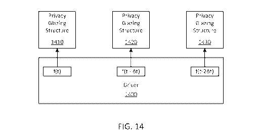
pulse (e.g., step
702) can include calculating a time-based value of a response, such as a
temporal derivative
or running average of a measured response (e.g., resulting voltage or current
value).
Additionally or alternatively, such response data can be filtered over time,
for example, to
remove noise, outliers, etc. from the data collected over time. Such a time-
based value can be
used to determine one or more electrical characteristics of the privacy
structure.
[0082] In some embodiments, the process shown in FIG. 7 is performed upon a
start-up
process of a privacy glazing structure, such as during an initial
installation. An installer may
connect the driver to a privacy glazing structure, and the driver may perform
the method
shown in FIG. 7 in order to establish and apply an initial drive signal for
the privacy glazing
structure. Such a process can be initiated manually and/or automatically. In
some examples,
the ability of the driver to determine and apply an appropriate electrical
drive signal for a
privacy glazing structure eliminates the need for different drivers to drive
different types of
privacy glazing structures, and enables loading an appropriate drive signal
without requiring
expertise of which drive parameters may be suitable for a given privacy
glazing structure.
[0083] FIG. 8 shows an exemplary categorization of electrical
characterizations of different
privacy glazing structures and corresponding electrical drive signal
parameters. As shown in
the exemplary illustration of FIG. 8, a structure can be categorized according
to a low or high
resistance value and a low or high capacitance value. In some examples, a
driver can be
- 19 -
CA 03138534 2021-10-28
WO 2020/223277
PCT/US2020/030358
programmed with threshold values to designate which resistance values are
"low" and which
are "high," and similarly, which capacitance values are "low" and which are
"high."
[0084] One category of privacy glazing structure shown in FIG. 8 includes a
low resistance
and a low capacitance. Such structures can include, for example, small
structures (e.g.,
contributing to a low capacitance value) having busbar contacts (e.g.,
contributing to a low
resistance value). In some cases, low resistance values can lead to large
current spikes when a
square wave or other sharp transitioning voltage signal is applied to the
structure.
Accordingly, a corresponding electrical drive signal can include one or more
features to
mitigate risks of a large current value, such as employing a maximum current
regulator,
utilizing a slew-rate square wave, and/or a pulse-width modulated (PWM) signal
(e.g., from
the rail voltage). In some examples, a lower-frequency electrical drive signal
can be used to
minimize average power consumption over time. One or more such features can
adequately
charge a small capacitive load (e.g., a capacitive electrically controllable
optically active
material in a privacy glazing structure) to provide proper aesthetic structure
behavior while
reducing large current spikes.
[0085] Another category of structure in the example of FIG. 8 comprises a low
resistance and
high capacitance structure, for example, a large structure (having a high
capacitance value)
and busbar contacts (contributing to a low resistance value). Such a structure
may also be
susceptible to large current spikes due to the low resistance, though the low
resistance can
facilitate filling the capacitance with charge quickly to provide high quality
aesthetics during
operation of the structure. Similar techniques can be employed to reduce the
risk of current
spikes, such as a maximum current regulator, a slew-rate square wave signal,
or applying a
PWM signal.
[0086] Another category of structure according to the example of FIG. 8
includes a high
resistance and a high capacitance, for example, a large structure having point
contacts (e.g.,
contributing to a higher resistance value). In some such instances, a large
resistance value
may limit current spikes, but also may make it more difficult to fill the
capacitance with
charge. Further, since the capacitance is large, it can require a large amount
of charge to
quickly charge the structure for good aesthetic behavior. Thus, in some
examples, an
electrical drive signal can include an overdriven square wave. For instance,
in some
embodiments, the electrical drive signal comprises a square wave in which a
portion of the
square wave is overdriven. In an exemplary implementation, within a square
wave pulse, the
first half of the pulse may be applied at a higher voltage than the second
half of the pulse in
order to more quickly fill the capacitance of the structure. Additionally or
alternatively, a
- 20 -
CA 03138534 2021-10-28
WO 2020/223277
PCT/US2020/030358
lower frequency waveform can be used in order to provide additional time for
the large
capacitance to be charged.
[0087] A fourth category of structure according to the example of FIG. 8
includes a high
resistance and a low capacitance, for example, a small structure having point
contacts. The
high resistance generally will reduce large current spikes, and the small
capacitance generally
allows for a relatively small amount of current necessary to fill the
capacitance with charge to
achieve good optical aesthetics. In some examples, such a structure can
operate with a
"default" electrical drive signal. In some embodiments, various electrical
parameters can be
adjusted and/or implemented to increase operation efficiency, such as
incorporating a voltage
slew-rate to mitigate excessive current peaks and minimize peak power
consumption and/or
reducing frequency to mitigate average power consumption.
[0088] While shown as two bins for two categories, it will be appreciated that
any number of
parameters may be analyzed, and may be distinguishable by any number of bins.
For
instance, in general, a group of N parameters (in FIG. 8, N = 2; resistance
and capacitance)
can be divided into M bins (in FIG. 8, M = 2; low and high) into which the
parameter values
may fall. Combinations of the characteristics and corresponding bins into
which they fall can
be used to identify (e.g., via equation or lookup table) an appropriate
electrical drive signal
for driving the privacy glazing structure having such characteristics.
[0089] In some examples, methods similar to that shown in FIG. 7 can be
repeated over time.
Such methods can be carried out manually or automatically (e.g., according to
a pre-
programmed schedule) in order to determine if a drive signal should be updated
based on
changes in one or more electrical characteristics of the privacy glazing
structure. In some
such examples, the existing drive signal may be stopped in order to execute a
method similar
to that shown in FIG. 7 to determine whether or not a drive signal should be
updated. This
can be performed manually or according to a schedule, for example, at night,
when
undesirable optical characteristics that may result from an interruption in
operation may go
unnoticed. In some such embodiments, various data can be stored in memory,
such as
determined characteristics of the privacy glazing structure based on the
response to the
applied sensing pulse. In some examples, characteristics of the privacy
glazing structure
determined at installation to establish an electrical drive signal are
associated with an initial
time to.
[0090] FIG. 9 shows a process-flow diagram for updating an electrical drive
signal provided
to a privacy glazing structure via an electrical driver. In an exemplary
implementation, the
method shown in FIG. 9 can be performed after a driver has been applying an
existing drive
- 21 -
CA 03138534 2021-10-28
WO 2020/223277
PCT/US2020/030358
signal to a privacy glazing structure. The method of FIG. 9 includes applying
an electrical
sensing pulse to a privacy glazing structure at a time tn (900), analyzing the
response of the
privacy glazing structure to the applied electrical sensing pulse (902), and
determining one or
more electrical characteristics of the privacy glazing structure at time tn
(904). The method
includes comparing the determined characteristics at time tn to
characteristics determined at a
previous time tn-i (906). If the change in the characteristic(s) at time tn
with respect to the
characteristic(s) at time tn-i is not greater than a threshold amount (908),
then the driver
continues to apply the existing electrical drive signal (910). If the change
in the
characteristic(s) between times tn-i and tn is/are greater than a threshold
amount (908), the
driver can be configured to load and/or update one or more drive parameters to
establish an
updated electrical drive signal (912).
[0091] In some embodiments, the updated electrical drive signal can be
determined based on
the determined electrical characteristics at time tn, similar to loading one
or more drive
parameters based on the determined characteristics as described with respect
to FIG. 7.
Additionally or alternatively, loading/updating one or more drive parameters
to establish the
updated electrical drive signal can comprise adjusting one or more drive
parameters based on
an amount of change detected for the one or more electrical characteristics.
[0092] With respect to FIG. 9, determining whether or not the change(s) in one
or more
electrical characteristics between times tn-i and tn is/are greater than a
threshold amount can
be performed in a variety of ways. In some embodiments, each characteristic(s)
includes a
corresponding absolute threshold difference that, if surpassed, causes a
change in the one or
more parameters of the electrical drive signal. For instance, in an exemplary
embodiment, if a
resistance value measured as one of the one or more electrical characteristics
changes by
more than 1000 Ohms, the change is considered to be greater than the
threshold. Additionally
or alternatively, a change greater than a threshold amount can correspond to a
percentage
change in a characteristic. For example, in some embodiments, one or more
drive parameters
can be updated in response to a resistance value increasing by at least 100%.
In another
example, one or more drive parameters can be updated in response to a
capacitance value
changing by at least 10%.
[0093] In some embodiments, change in each of the one or more parameters over
time can be
compared to a corresponding threshold. In some examples, if any one
characteristic differs
from its previous value by a corresponding threshold amount, the change in
characteristic(s)
is considered to be greater than the threshold amount, and an updated
electrical drive signal is
established. In other examples, the amount of change in each of the one or
more
- 22 -
CA 03138534 2021-10-28
WO 2020/223277
PCT/US2020/030358
characteristics must be greater than a corresponding threshold amount in order
for the change
to be considered greater than a threshold and to update an electrical drive
signal. In various
embodiments, different combinations of electrical characteristics (e.g., a
subset of a plurality
of determined characteristics) can be analyzed to determine whether or not the
change in the
characteristics is greater than a threshold amount.
[0094] In some embodiments, loading/updating one or more drive parameters
(912) can be
based on additional tracked/measured data 914. Tracked/measured data 914 can
include
information such as the age of the privacy glazing structure, the temperature
of the privacy
glazing structure, or the like. In some examples, the driver can be configured
to adjust one or
more drive parameters based on such data.
[0095] For instance, in an exemplary embodiment, in the event that the
change(s) in one or
more electrical characteristics between times tn-i and tn is/are greater than
a threshold amount,
the driver can be configured to acquire temperature information (e.g.,
structure and/or
environment temperature information) and update the one or more drive
parameters based on
the temperature information. Temperature information can be received, for
example, from a
contact (e.g., thermocouple) or non-contact (e.g., infrared) temperature
measurement device
that outputs temperature information representative of the structure itself
Additionally or
alternatively, temperature information can be received from an ambient
temperature sensor.
In some examples, one or more temperature sensors can be associated with each
of one or
more privacy glazing structures in a privacy system. For example with respect
to FIG. 6,
temperature sensors 312, 322, 332 can be configured to provide temperature
information
(e.g., contact and/or environmental temperature information) associated with
corresponding
privacy glazing structures 310, 320, 330, respectively.
[0096] In addition or alternatively to temperature information, if the
change(s) in one or more
electrical characteristics between times tn-i and tn is/are greater than a
threshold amount, the
driver can be configured to determine the age of the privacy glazing structure
and update one
or more drive parameters based upon the age of the structure. In some
examples, a driver can
be configured to flag a structure as aging, for example, when the structure
has been in
operation for a predetermined amount of time and/or when the electrical
characteristics are
representative of an aging structure. Age and/or temperature can be used in
addition or
alternatively to the determined electrical characteristics when determining an
updated
electrical drive signal.
[0097] As described with respect to FIGS. 7 and 9, in various processes, the
driver can be
configured to apply an electrical sensing pulse to a privacy glazing structure
for
- 23 -
CA 03138534 2021-10-28
WO 2020/223277
PCT/US2020/030358
characterizing the structure (e.g., determining one or more electrical
characteristics thereof).
In some examples, the characterizing the structure comprises determining one
or more
electrical parameters of the structure, such as a resistance, a capacitance,
etc., and in some
such examples, comprises determining an equivalent circuit representative of
the structure's
electrical properties (e.g., an RC circuit, an RLC circuit, etc.).
[0098] In various embodiments, different electrical sensing pulses can be used
to determine
such characteristics. For instance, in various examples, an electrical sensing
pulse can include
a DC sense pulse, a low frequency drive signal (e.g., a signal having similar
characteristics,
such as amplitude or waveform, of a drive signal but having lower frequency),
or an
operational drive signal (e.g., a currently-implemented drive signal). In some
embodiments, a
user may select which type of electrical sensing pulse to use when
characterizing a privacy
glazing structure.
[0099] In some cases, a DC sense pulse can provide the most accurate
characterization, since
the DC signal can be applied over several RC time constants of the structure.
In some
embodiments, the DC pulse is applied to a structure for at least five time
constants, but can
also be applied for longer amounts of time, such as for at least 10 time
constants, at least 100
time constants, at least 1000 time constants, or other values. While the exact
value of an RC
time constant may not be known a priori, in some examples, a privacy glazing
structure can
have an expected range of time constants (e.g., associated with different
structure sizes, types,
etc.) that can be used to determine, for example, a minimum DC pulse length to
increase the
likelihood that the DC sense pulse lasts at least a minimum number of time
constants. A
potential drawback to a DC sense pulse is that during the pulse, the visual
aesthetics of the
privacy glazing structure may degrade. However, this type of electrical
sensing pulse can be
used during, for example, an installation procedure or when the structure is
not in use, a
temporary decline in the aesthetic appearance of the structure may be
acceptable.
[0100] In some examples, an operational drive signal can be used as an
electrical sensing
pulse, such as one of the drive signals shown in FIGS. 4A and 4B. In an
exemplary
embodiment, such a drive signal can be applied at a frequency of between
approximately 45
and 60 Hz. In some such examples, such a frequency generally results in pulses
that are too
short to reach several RC time constants for structure characterization, and
as a result, may
provide a less accurate characterization when compared to a longer DC sense
pulse.
However, since the operational drive signal doubles as the electrical sensing
pulse, no
aesthetic degradation occurs during the characterization process. Thus,
characterization using
- 24 -
CA 03138534 2021-10-28
WO 2020/223277
PCT/US2020/030358
the operational drive signal as an electrical sensing pulse can be performed
during the
daytime when the chances of being viewed are high.
[0101] In some cases, a low frequency drive signal can provide a balance
between the DC
sense pulse and the operation drive signal as a sense pulse. For example, in
some
embodiments, reducing the frequency of the drive signal provides added time
for
characterizing the response of the privacy glazing structure to the signal
while not impacting
the aesthetics of the privacy glazing structure as severely as a longer DC
sense pulse. In some
examples, a low frequency drive signal has a frequency range between
approximately 5 and
45 Hz. In some cases, the low frequency drive signal still reduces the
aesthetics of the privacy
glazing structure, and so may be suitable for applying at night when it is
unlikely that the
privacy glazing structure will be viewed with temporarily reduced aesthetics.
[0102] In various embodiments, a user may manually initiate a privacy glazing
structure
characterization process in which one or more electrical sensing pulses is
applied to the
privacy glazing structure determining one or more electrical characteristics
of the structure,
for example, to determine or update an electrical drive signal. In some such
examples, a user
may select from a plurality of available electrical sensing pulse types, such
as those described
elsewhere herein. Additionally or alternatively, in some examples, a driver
can be configured
to automatically perform a characterization process, for example, according to
a
predetermined schedule (e.g., once per hour, once per day, once per week,
etc.). In some such
examples, a driver can be configured to perform different characterization
processes
according to when the process is carried out. For instance, upon initial
installation, a driver
can apply a DC sense pulse to initially characterize the structure and
establish an electrical
drive signal.
[0103] After installation, the driver can be configured to periodically apply
an electrical
sensing pulse to characterize the structure, for example, to determine if one
or more
characteristics of the structure have changed and/or if an electrical drive
signal should be
updated, such as described with respect to FIG. 9. In some such examples, the
driver can be
configured to select an electrical sensing pulse to apply, for instance,
depending on a time of
day or other factors. For example, in some embodiments, the driver can be
configured to
apply a low frequency drive signal electrical sensing pulse, such as described
elsewhere
herein, if the electrical sensing pulse is applied during one or more
predetermined intervals,
such as when temporary aesthetic degradation may not be noticed. Outside of
the
predetermined time intervals, for example, when temporary aesthetic
degradation may be
noticed, the driver can be configured to apply an electrical sensing pulse
that is the
- 25 -
CA 03138534 2021-10-28
WO 2020/223277
PCT/US2020/030358
operational drive signal to reduce or eliminate the impact on the structure
aesthetics during a
characterization process.
[0104] In some examples, different update schedules may be implemented
according to the
processing capabilities of the system components used for performing the
analysis. For
instance, in some embodiments, on-board processing components may have limited
processing ability, and may perform such analysis less frequently than a cloud-
based
processing system with greater processing resources.
[0105] In some examples, periodic characterization of a privacy glazing
structure over time
can be used to track structure operation and aging characteristics or to
adjust the electrical
drive signal to accommodate for changing characteristics, for example, as
described with
respect to FIG. 9. In some embodiments, determined one or more electrical
characteristics
captured at a plurality of times can be saved in memory, for example, for
comparison (e.g., as
described with respect to FIG. 9), trend analysis, etc. In some examples, the
driver can be
configured to perform statistical analysis of the electrical characteristics
over time and
recognize patterns. Patterns can include trending of one or more electrical
characteristics in a
given direction over time (e.g., due to structure breakdown, etc.), repeating
trends (e.g.,
electrical characteristics changing during daylight and nighttime hours or
changing over
seasons as ambient temperatures change, etc.). In some cases, the driver can
similarly track
and/or analyze additional data, such as ambient or structure temperature data,
and can be
configured to correlate electrical characteristics with such additional data.
[0106] Additionally or alternatively, in some implementations, the driver can
be configured
to periodically characterize aspects of the privacy glazing structure at a
different rate
throughout the life cycle of the structure. For example, in some cases, the
driver characterizes
the structure more frequently shortly after installation while the driver
learns the behavior
and/or typical characteristics of the structure, for example, environmental
impacts (e.g.,
temperature, sunlight, etc.) on structure behavior.
[0107] In some examples, the driver can be configured to detect or predict an
environmental
change (e.g., a temperature change, a change in ambient light, etc.), and can
characterize the
structure within a short time span (e.g., within minutes or hours) to isolate
impacts of certain
factors. For example, a driver can be configured to characterize a structure
when the sun is
blocked by a cloud and then again once the sun is no longer blocked in order
to isolate the
impact of daylight on the structure characteristics. The driver can be
configured to detect
such changes, for example, via one or more sensors and/or via data analysis
(e.g., via internet
access to weather data).
- 26 -
CA 03138534 2021-10-28
WO 2020/223277
PCT/US2020/030358
[0108] Similarly, in an example implementation, a driver can be configured to
detect and/or
predict an earthquake (e.g., via intern& connectivity to an earthquake
notification system
and/or one or more accelerometers or other sensors). The driver can be
configured to
characterize the structure after a detected earthquake to assess for damage or
changing
operating characteristics. If the driver receives information (e.g., from a
notification system)
that an earthquake is imminent, the driver can characterize the structure
prior to the
occurrence of the earthquake and again after the earthquake to specifically
detect changes in
structure characteristics due to the earthquake.
[0109] In some embodiments, the driver can be configured to recognize patterns
in electrical
characteristics of the privacy glazing structure over time and/or correlate
electrical
characteristics of the privacy glazing structure with other data, such as
ambient or structure
temperature data. In some such examples, the driver can be configured to
adjust/update one
or more drive parameters for an electrical drive signals according to the
statistical analysis
and recognized patterns and/or correlations. For example, the driver may be
configured to
automatically switch between summer and winter electrical drive signals based
on a
recognized change in structure behavior over time. Additionally or
alternatively, the driver
can be configured to adjust one or more drive parameters based on received
data, such as
temperature data, based on an observed correlation between temperature data
and structure
characteristics.
[0110] Electrical events, such a detected arcing event within the structure, a
power surge, a
power outage, a lightning strike, or other events can trigger the driver to
perform a
characterization in order to detect changes and/or damage to the structure.
[0111] In some examples, various electrical drive signal parameters can be
adjusted based on
tracked and/or measured data, such as aging data and/or temperature data. In
some
embodiments, such parameters can include voltage (e.g., RMS voltage and/or a
peak
voltage), frequency, and/or a rise time/slew rate. In various examples,
loading/updating one
or more drive parameters (e.g., step 912 in FIG. 9) comprises one or more of:
[0112] decreasing a voltage value in response to a temperature increase
[0113] increasing a voltage value in response to a temperature decrease
[0114] increasing a voltage value as the structure age increases
[0115] decreasing a frequency value in response to a temperature increase
[0116] increasing a frequency value in response to a temperature decrease
[0117] decreasing a frequency value as the structure age increases
[0118] lengthening a slew rate/rise time in response to a temperature increase
- 27 -
CA 03138534 2021-10-28
WO 2020/223277
PCT/US2020/030358
[0119] shortening a slew rate/rise time in response to a temperature decrease
[0120] shortening a slew rate/rise time as the structure age increases.
[0121] Alternatively or in addition to factors such as aging and
temperature/seasonal changes
in the operation of a privacy glazing structure, other factors, such as a
structure health metric,
can be analyzed. In some embodiments, a health metric includes a measure of a
leakage
current through the structure. Leakage current can result from a plurality of
issues, such as
breakdown in a structure material, such as optically active material 18, a
poor or breakdown
coating, or other volatile portion of a structure. Leakage current can be
measured in a variety
of ways. In an exemplary embodiment, a leakage current value can be determined
based on
analysis of a current flowing through the privacy glazing structure during a
particular time.
[0122] FIGS. and 10A and 10B show exemplary drive signal and resulting
response current
signal over time for a privacy glazing structure. As shown, a slew-rate square
wave voltage
applied to the privacy glazing structure results in a periodic current
response. While the
signals are not necessarily shown on the same scale in FIGS. 10A and 10B, it
is apparent that
the shape of the current signal through the privacy glazing structure is
different between FIG.
10A and FIG. 10B. Such differences can indicate changes in a leakage current
flowing
through the privacy glazing structure.
[0123] FIGS. 11A and 11B show zoomed-in views of the exemplary current and
voltage
signals of FIGS. 10A and 10B, respectively, including different display scales
for ease of
display.
[0124] In some embodiments, one or more metrics associated with the current
signal can be
measured during a time when a structure is known to be in good working
condition, such as
upon installation of the structure. Such metrics can include, for example, a
time derivative or
integral of the measured current at or over a predetermined portion of the
drive signal (e.g.,
during a positive voltage pulse, etc.). Additionally or alternatively, a
difference in an
equilibrium current during positive and negative portions of the square wave
(shown as Ai
and A2 in FIGS. 11A and 11B, respectively) can be used as a metric. For
instance, in some
embodiments, a measured current response to the applied electrical drive
signal comprises
measuring a current response during a predetermined portion of the applied
drive signal, such
as a period of time between transitions in an applied square wave. In some
examples, this can
avoid comparisons of current responses that include features (e.g., inrush
currents) that may
be present regardless of the condition of the structure.
[0125] One or more current response metrics can be recorded over time in order
to determine
one or more leakage current values associated with the structure. FIG. 12
shows a process
- 28 -
CA 03138534 2021-10-28
WO 2020/223277
PCT/US2020/030358
flow diagram showing an exemplary process for determining one or more leakage
current
values. In some examples, the method in FIG. 12 can be carried about via the
driver of a
privacy glazing structure. The method includes measuring a value associated
with a current
response signal for a healthy structure at an initial time to (1200). Such
measuring can include
determining a derivative or integral of the current and/or a difference
between equilibrium
currents during positive and negative portions of an applied alternating drive
signal (e.g., a
square wave). In some examples, time to generally corresponds to a time when
the structure is
assumed to be at peak or near-peak health, such as during installation or
initial operation.
[0126] Next, the method includes again measuring a value associated with the
current
response signal at a time tn (1202), which, in a first instance after time to,
may be denoted ti
(n=1). For instance, in some examples, the first measurement after the initial
measurement at
time to is performed at time ti. The method includes determining a leakage
current at time tn
based on determined values associated with the current signal at times to and
tn (1204). For
instance, in some examples, determining the leakage current comprises
determining the
difference in the measured value at time tn vs. time to in order to determine
the change caused
by any leakage current that has developed since the measurement of the value
for the healthy
structure at time to. In various examples, such determination can be performed
locally, for
example via the driver, or can be done via cloud-based computing.
[0127] The method of FIG. 12 includes determining if the leakage current
satisfies a
predetermined condition (1206). If the leakage current does not satisfy the
predetermined
condition, the driver continues to apply an existing electrical drive signal
(1208). For
instance, in some examples, the leakage current not satisfying the
predetermined condition
can indicate that there is no leakage current present or the leakage current
is small enough so
that the existing electrical drive signal can adequately drive the privacy
glazing structure
without visible optical degradation. In some such cases, the drive signal does
not need to be
altered to compensate for excess leakage current.
[0128] However, in some examples, if the leakage current does satisfy the
predetermined
condition, the method can include the step of loading and/or updating one or
more drive
parameters to establish an updated electrical drive signal (1210). For
instance, in some
examples, excess leakage current can degrade the optical performance of a
privacy glazing
structure, but can be compensated for via adjustments to the electrical drive
signal.
[0129] Example adjustments to an electrical drive signal based on excess
leakage current can
include increasing a voltage (1212), decreasing a frequency (1214), and/or
pulsing a voltage
(1216). In some examples, increasing a voltage (e.g., the value of VA in FIG.
4) can
- 29 -
CA 03138534 2021-10-28
WO 2020/223277
PCT/US2020/030358
compensate for lost voltage due to the leakage current. Decreasing frequency
provides
additional time for a capacitive optically active material to charge, for
example, during a
positive portion of a square wave drive signal. In some examples, decreasing a
frequency of
the electrical drive signal comprises increasing a period of the electrical
drive signal. For
instance, with respect to the example electrical drive signal shown in FIG.
4A, adjusting an
electrical drive signal comprises increasing the amount of time that the
voltages VA and -VA
are applied during each cycle.
[0130] With respect to voltage pulsing, in some examples, a drive signal
includes one or
more floating steps, in which the optically active material is disconnected
from power and
ground. For instance, with respect to FIG. 5, in some examples, a drive signal
can include a
period of time during which, for example, all switches SW1, SW2, SW3, and SW4
are
opened so that the load (e.g., the optically active material between contact
electrodes)
maintains its current voltage. However, leakage current may cause the voltage
at the load to
sag during the floating step. Pulsing the voltage (e.g., step 1216) can
include modifying the
electrical drive signal to include applying one or more voltage pulses to the
load during one
or more floating steps in order to maintain a voltage at the load and
compensate for voltage
sagging due to leakage current. In an example implementation, a drop in
voltage from an
expected value (e.g., a voltage sag) across the structure can be measured and
compared to a
predetermined threshold. If the drop in the voltage meets or exceeds the
predetermined
threshold, a rail voltage pulse can be applied to the load. The frequency of
applying the rail
voltage pulse can depend on the severity of the sag (e.g., due to the severity
of a leakage
current). For example, in some cases, the rail voltage pulse can be applied
multiple times in a
single cycle or half cycle of the applied electrical drive signal.
[0131] In various embodiments, the index n can be incremented, and steps in
the process of
FIG. 12 can be repeated for a plurality of times ti, t2,..., tN. In some
examples, measured
values and/or leakage current values associated with one or more times (e.g.,
at any one or
more of times to... tN) can be saved to memory. Additionally or alternatively,
the method can
include generating a measurement curve of the measured leakage current vs.
time and/or vs.
index. In some examples, a trend of leakage current over time can be used to
determine
information regarding a likely cause of the leakage current.
[0132] In some embodiments, determining if the leakage current satisfies a
predetermined
condition (e.g., step 1206) can include determining if a single leakage
current value satisfies a
condition, such as a determined leakage current exceeding a threshold leakage
current value
or falling within a predetermined range of leakage current values.
Additionally or
- 30 -
CA 03138534 2021-10-28
WO 2020/223277
PCT/US2020/030358
alternatively, determining if the leakage current satisfies a predetermined
condition can
include determining if a trend of leakage current vs. time and/or time index
satisfies a
predetermined condition, such as if the derivative of the leakage current over
time exceeds a
predetermined threshold.
[0133] In some embodiments, one or more actions can be taken in response to
the leakage
current satisfying a predetermined condition, such as shown in steps 1212,
1214, and 1216. In
some instances, different such actions or combinations thereof can be
performed in response
to different leakage current conditions, such as a leakage current value
falling into different
predetermined ranges and/or a leakage current trend over time satisfying one
or more
predetermined conditions. In some embodiments, leakage current compensation
can be
initiated and/or modified by a user in the event that the privacy glazing
structure has optically
degraded.
[0134] In some examples, non-linearities in the current response with respect
to an applied
voltage can be attributed to ion behavior in the privacy glazing structure. In
some such
examples, such non-linear responses can be analyzed to determine various
parameters, such
as various sizes and/or densities of ions moving in the structure and the
response of such ions
to the applied electric field in the structure. In some embodiments, such
information can be
used to determine details regarding the optically active material and how such
material is
breaking down during operation causing optical degradation of the privacy
glazing structure.
In some embodiments, data of leakage current over time can be used to
determine one or
more leakage current sources, such as bad coatings, ion generation, and/or
other factors.
[0135] Various such calculations and/or determinations can be performed
locally, for
instance, via the driver, and/or can be performed in an external environment,
such as via
cloud-based computing.
[0136] As described with respect to FIG. 6, a single driver 300 can be
configured to provide
electrical drive signals to each of a plurality of privacy glazing structures
(e.g., 310, 320, 330)
for simultaneous operation of such structures. As described herein, a driver
can be configured
to determine electrical characteristics of a privacy glazing structure in
order to establish an
electrical drive signal appropriate for driving such a structure. In some
embodiments, a driver
can be configured to perform various such processes (e.g., as shown in FIGS.
7, 9, and/or 12)
for each of a plurality of associated privacy glazing structures. A driver can
be configured to
determine an appropriate electrical drive signal for each of a plurality of
privacy glazing
structures, and provide such electrical drive signals to each such privacy
glazing structure
simultaneously.
-31 -
CA 03138534 2021-10-28
WO 2020/223277
PCT/US2020/030358
[0137] As described elsewhere herein, in some examples, the electrical drive
signal
comprises a square wave or an approximately square wave (e.g., a square wave
having a slew
rate, a trapezoidal wave, a square wave shape having a slow zero-crossover,
etc.) signal. For
instance, the exemplary voltage vs. time drive signals shown in FIGS. 4, 10A,
and 10B show
an approximate square wave drive signal. Further, as shown in FIGS. 10A and
10B,
transitions that occur every half-period in the square wave drive signal
results in a spike in
the current through the structure. In general, given a capacitive privacy
glazing structure, the
steeper the edge of the square wave drive signal, the larger the corresponding
current spike is
likely to be. Thus, if a plurality of privacy glazing structures are being
driven simultaneously
with square wave or approximate square wave drive signals, current spikes in
each structure
may occur at approximately the same time, creating a large current/power peaks
output from
the driver.
[0138] In some embodiments, the driver is configured to stagger the electrical
drive signals
applied to one or more privacy glazing structures to reduce the peak
current/power draw
associated with the current response to the applied electrical drive signals.
Put differently,
staggering the electrical drive signals can be done so that the peak current
drawn by each of
the privacy glazing structures driven by the driver occurs at different times.
In some
embodiments, staggering a second electrical drive signal with respect to a
first electrical drive
signal comprises delaying the application of the second electrical drive
signal with respect to
the application of the first electrical drive signal when the first and second
electrical drive
signals are in phase with one another. In some examples, staggering a second
electrical drive
signal with respect to a first electrical drive signal comprises applying the
first and second
electrical drive signals substantially simultaneously while phase-shifting the
second electrical
drive signal relative to the first electrical drive signal. In still further
embodiments, staggering
a second electrical drive signal with respect to a first electrical drive
signal comprises phase
shifting the second electrical drive signal with respect to the first
electrical drive signal and
temporally delaying the application of the second electrical drive signal with
respect to the
application of the first electrical drive signal. Thus, in various
embodiments, staggering
electrical drive signals can include phase-shifting a signal, temporally
delaying the
application of a signal, or combinations thereof
[0139] FIG. 13 shows a process flow diagram showing an example process for
applying
staggered electrical drive signals to a plurality of privacy glazing
structures. The method
includes applying an electrical sensing pulse to each of a plurality of
privacy glazing
structures (1300) and determining an electrical drive signal for each of the
plurality of
- 32 -
CA 03138534 2021-10-28
WO 2020/223277
PCT/US2020/030358
privacy glazing structures (1302). Such steps can be performed for each of the
privacy
glazing structures, for example, as described with respect to FIG. 7.
[0140] The method of FIG. 13 further includes determining a stagger amount for
one or more
of the privacy glazing structures (1304). Such determining can be performed in
a variety of
ways. In some examples, the driver can be configured to provide a
predetermined amount of
delay between the electrical drive signals for each privacy glazing structure.
Additionally or
alternatively, in some examples, the driver can be configured to analyze the
determined
plurality of electrical drive signals in order to determine an appropriate
amount of stagger for
applying the plurality of electrical drive signals. For instance, one or more
parameters of each
electrical drive signal, such as magnitude, frequency, and the like, can be
analyzed to
determine an appropriate amount of stagger between the electrical drive
signals, for example,
to reduce instances of signal superposition that can result in large current
and/or power
spikes. In some embodiments, frequency content of a first electrical drive
signal and a second
electrical drive signal can be compared in order to determine an offset
between the first and
second electrical drive signals to reduce or eliminate superposition of one or
more features of
the drive signals, such as transitions between states in square wave drive
signals.
[0141] In some examples, each of the plurality of electrical drive signals for
the
corresponding plurality of privacy glazing structures is staggered with
respect to the other
signals so that no two signals are applied simultaneously. In other examples,
the driver may
determine that two or more electrical drive signals can be applied
simultaneously without
resulting in an undesirable current spike (e.g., resulting in a total current
draw, such as a peak
current draw, exceeding a predetermined threshold). In some such examples, the
driver can
be configured to provide such electrical drive signals simultaneously while
potentially
staggering other electrical drive signals.
[0142] The method of FIG. 13 further includes applying an electrical drive
signal to each of
the plurality of privacy glazing structures including the determined stagger
amounts (1306).
Including the stagger amounts in applying an electrical drive signal can
include delaying the
application of a determined electrical drive signal and/or phase-shifting the
electrical drive
signal. As described, in some cases, determined stagger amounts can result in
multiple
electrical drive signals (e.g., a subset of a plurality of applied electrical
drive signals) being
applied to corresponding privacy glazing structures simultaneously and in-
phase with one
another while other signals are staggered with respect to the simultaneously-
applied signals.
In other examples, each electrical drive signal is delayed and/or phase-
shifted with respect to
each of the other electrical drive signals.
- 33 -
CA 03138534 2021-10-28
WO 2020/223277
PCT/US2020/030358
[0143] In some embodiments, the driver can be configured to adjust one or more
electrical
drive signals in order to better stagger such signals. For instance, as
represented by the
broken lines in FIG. 13, a driver can be configured to determine a stagger
amount (1304)
based on adjusted electrical drive signals (e.g., different electrical drive
signals than
determined via the method of FIG. 7). Thus, in some such embodiments, the
driver can be
configured to determine updated electrical drive signals (1302) after
determining appropriate
stagger amounts to reduce peak current and/or power loads on the driver. In an
exemplary
embodiment, if a first privacy glazing structure is to be driven with an
electrical drive signal
having a first frequency and a second privacy glazing structure is to be
driven with an
electrical drive signal having a second frequency different from the first.
Staggering such
signals by a phase shift and/or delay may reduce the current spikes associated
with the initial
application of the respective electrical drive signals. However, superposition
of such
electrical drive signals may nevertheless result in times at which undesirably
large current
and/or power spikes occur. In some examples, the driver can be configured to
adjust one or
both such electrical drive signals to reduce or eliminate such instances, such
as adjusting the
electrical drive signals to include a common frequency and/or adjusting the
magnitude of one
or both signals so that combined current and/or power spikes remain below a
threshold level.
Other techniques for adjusting one or more electrical drive signals for
corresponding one or
more privacy glazing structures in response to staggering analysis are
possible. In some such
examples, upon adjusting one or more such electrical drive signals to reduce
instances of
undesirably large current and/or power spikes, the determined electrical drive
signals
including the determined stagger amounts can be applied to respective privacy
glazing
structures (1306).
[0144] FIGS. 14 and 15 show example implementations of applying electrical
drive signals
including determined amounts of stagger to a plurality of privacy glazing
structures. FIG. 14
shows a driver 1400 in electrical communication with privacy glazing
structures 1410, 1420,
and 1430. In the illustrated example of FIG. 14, a driver 1400 provides a
common electrical
drive signal f(t) to each of privacy glazing structure 1410, 1420, and 1430.
For example, each
privacy glazing structure 1410, 1420, and 1430 could be the same type of
structure, include
similar electrical characteristics, or the like, in order to result in the
same general electrical
drive signal to be applied to each structure, such as determined via the
method of FIG. 7.
[0145] As shown in FIG. 14, the electrical drive signal f(t) is phase-shifted
between each
privacy glazing structure to reduce or eliminate current spikes at each
structure
simultaneously. For instance, while signal f(t) is provided to privacy glazing
structure 1410,
- 34 -
CA 03138534 2021-10-28
WO 2020/223277
PCT/US2020/030358
signal f(t-At) is applied to privacy glazing structure 1420. Thus, various
elements of the
electrical drive signals and the resulting current response (e.g., current
spikes) will be delayed
by an amount At in privacy glazing structure 1420 with respect to privacy
glazing structure
1410. Similarly, signal f(t-2At) is applied to privacy glazing structure 1430,
such that
elements of the electrical drive signal and resulting current response will be
delayed by At in
privacy glazing structure 1430 with respect to privacy glazing structure 1420,
and by 2At
with respect to privacy glazing structure 1410.
[0146] In some examples, the amount of stagger between each of the plurality
of electrical
drive signals is within one period of the electrical drive signal. For
example, if the system in
FIG. 14 includes privacy glazing structures 1410, 1420, and 1430, and
electrical drive signal
f(t) is periodic with a period of T, in some instances, 2At < T. For instance,
if the frequency
of the electric drive signal f(t) is 60 Hz, then in some examples, At < 8.3
ms. In still further
examples, the amount of stagger between each of the plurality of electrical
drive signals is
within a half period of the electrical drive signal.
[0147] FIG. 15 shows a driver 1500 providing electrical drive signals to each
of a plurality of
privacy glazing structures 1510, 1520, and 1530. As shown, in some examples,
different
electrical drive signals f(t), g(t), and h(t) can be provided to the privacy
glazing structures
1510, 1520 and 1530, respectively. Such electrical drive signals can be
determined for each
privacy glazing structure, for example, via the method shown in FIG. 7.
Different electrical
drive signals can include one or more different parameters, such as peak
voltage, slew rate,
wave shape, frequency, and the like. As described elsewhere herein, in some
examples, the
driver can determine an amount of stagger to apply between different
electrical drive signals,
for example, based on mathematical analysis of the determined electrical drive
signals. In the
illustrated example, the electrical drive signal g(t) applied to privacy
glazing structure 1520 is
staggered with respect to electrical drive signal f(t) by an amount Ati and
the electrical drive
signal h(t) applied to privacy glazing structure 1530 is staggered with
respect to electrical
drive signal f(t) by an amount At2. In various examples, At can be greater
than, less than, or
equal to At2 according to the determined amount(s) of stagger based on the
determined
electrical drive signals. As described elsewhere herein, in some examples,
different electrical
drive signals can be applied simultaneously (e.g., Ati = 0, At2= 0, and/or Ati
= At2) if the
driver determines that the combined current response to such electrical drive
signals would
not amount to an undesirably large current and/or power spike (e.g., greater
than a
predetermined threshold), for example, due to certain load sizes provided by a
plurality of
such privacy glazing structure.
- 35 -
CA 03138534 2021-10-28
WO 2020/223277
PCT/US2020/030358
[0148] FIGS. 16A-16C show example voltage vs. time profiles for a plurality of
electrical
drive signals used to drive a corresponding plurality of privacy glazing
structures in a system.
FIG. 16A shows a function f(t). FIG. 16B shows function f(t) delayed by a time
At, such that
the resulting signal can be represented by f(t-At). Similarly, FIG. 16C shows
function f(t)
delayed by a time 2At, such that the resulting signal can be represented by
f(t-2At). In the
illustrated example of FIGS. 16A-16C, an electrical drive signal f(t) is
applied to separate
privacy glazing structures with incorporated staggering so that various
transition portions of
each electrical drive signal that may cause individual current and/or power
spikes do not
happen simultaneously.
[0149] In some embodiments, once a plurality of drive signals are determined,
the driver can
determine which electrical drive signals, when applied simultaneously, cause
one or more
parameters (e.g., current spike values) to exceed a predetermined threshold.
Similarly, the
driver can determine which electrical drive signals, when combined, do not
cause the one or
more parameters to exceed the predetermined threshold(s). The driver can
determine which
electrical drive signals can be applied simultaneously and stagger the
application of electrical
drive signals or groups of electrical drive signals such that the one or more
parameters do not
exceed the predetermined threshold(s) when each electrical drive signal or
group of electrical
drive signals are applied.
[0150] In an example embodiment, a driver is connected to power five privacy
glazing
structures, three of which represent a maximum load that can be driven by the
driver. The
remaining two privacy glazing structures are considered small, and can be
driven
simultaneously without any electrical parameters exceeding a predetermined
threshold. The
driver can be configured to provide electrical drive signals to the two
smaller loads
simultaneously and in phase with one another, while staggering delivery of
each of the
remaining three electrical drive signals to the remaining structures.
[0151] While shown in FIGS. 14, 15, and 16A-C as including three privacy
glazing
structures, in general, systems can include a driver and any number of privacy
glazing
structures in communication therewith. The driver can be configured to perform
various
processes described herein for each of one or more privacy glazing structure
in electrical
communication therewith. In some examples, the driver can be configured to
determine the
number of privacy glazing structures to be provided with electrical drive
signals. Such a
determination can be used in determining various information, such as
determining
appropriate electrical drive signals and/or staggering amounts for driving the
one or more
privacy glazing structures.
- 36 -
CA 03138534 2021-10-28
WO 2020/223277
PCT/US2020/030358
[0152] Drivers can be configured to carry out processes as described herein in
a variety of
ways. In some examples, a system driver can include one or more components
configured to
process information, such as electrical signals and/or other received sensor
information, and
perform one or more corresponding actions in response thereto. Such components
can
include, for example, one or more processors, application specific integrated
circuits
(ASICs), microcontrollers, microprocessors, field-programmable gate arrays
(FPGAs), or
other appropriate components capable of receiving and output data and/or
signals according
to a predefined relationship. In some examples, the driver can include or
otherwise be in
communication with one or more memory components, such as one or more non-
transitory
computer readable media programmed with instructions for causing one or more
such
components to carry out such processes. Additionally or alternatively, the
driver can
communicate with additional devices, such as external computer systems and/or
networks to
facilitate information processing, such as cloud-based computing.
[0153] Various non-limiting examples have been described herein. Those having
ordinary
skill in the art will understand that these and others fall within the scope
of the appended
claims.
- 37 -