Note: Descriptions are shown in the official language in which they were submitted.
Lida r receiving unit
The present invention relates to a lidar receiving unit in a focal plane array
arrangement. The present invention furthermore relates to a lidar measuring de-
vice for detecting an object in an environment of a vehicle.
Modern vehicles (cars, vans, lorries) motorcycles, driverless transport sys-
tems, etc.) comprise a multiplicity of systems, which provide a driver or
operator
with information and/or control individual functions of the vehicle in a
partially or
fully automated manner. The environment of the vehicle and, if appropriate,
other
road users are detected by means of sensors. Based on the detected data, a
model
of the vehicle environment can be created and it is possible to react to
changes in
this vehicle environment. Due to the ongoing development in the field of
autono-
mously and partially autonomously driving vehicles, the influence and the
range of
effectiveness of advanced driver assistance systems (ADAS) and autonomously op-
erating transport systems are becoming ever greater. Due to the development of
ever more precise sensors, it is possible to detect the environment and to
control
individual functions of the vehicle completely or partially without the
intervention
of the driver.
An important sensor principle for the detection of the environment in this
case is lidar (light detection and ranging) technology. A lidar sensor is
based on the
emission of light pulses and the detection of the reflected light. A distance
to the
location of the reflection can be calculated by means of a time of flight
measure-
ment. A detection of a target can take place by evaluating the received
reflections.
With regards to the technical realization of the corresponding sensor, a
distinction
is made between scanning systems, which for the most part function on the
basis
of micromirrors, and non-scanning systems, in which a plurality of emitting
and
receiving elements are arranged statically side by side (in particular what is
known
as a focal plane array arrangement).
1
CA 03140197 2021-11-30
In this context, a method and a device for optical distance measurement are
described in WO 2017/081294 Al. The use of an emission matrix for emitting
measuring pulses and a reception matrix for receiving the measuring pulses is
dis-
closed. Subsets of the emission elements of the emission matrix are activated
dur-
ing the emission of the measuring pulses.
One challenge in the field of non-scanning lidar measuring systems lies in
the arrangement of the sensor elements in a reception array and in routing the
signals of the sensor elements to the edge of the reception array. On the one
hand,
a highest possible density of the sensor elements of the array should be
achieved.
On the other hand, an efficient routing of the signals to the edge of the
array for
further processing should be enabled. In addition, a high resolution or a good
de-
tection should be ensured.
On this basis, it is the object of the present invention to provide an
approach
for the efficient reading of an array of sensor elements. In particular, an
array
should be realized, in which blind regions are avoided to the greatest extent
pos-
sible. In addition, a high resolution should be achieved.
To achieve this object, the invention relates in a first aspect to a lidar
receiv-
ing unit in a focal plane array arrangement, having:
a multiplicity of sensor elements for receiving light pulses of a lidar
emitting
unit; and
a plurality of routing channels for transporting signals of the sensor ele-
ments to an edge region of the lidar receiving unit, wherein
in each case a plurality of sensor elements are arranged in a macro cell,
which is allocated to an emission element of the lidar emitting unit;
in each case a plurality of macro cells form a macro cell cluster and in each
case a plurality of macro cell clusters are arranged in a plurality of rows;
and
2
CA 03140197 2021-11-30
the routing channels cross the plurality of rows in each case between adja-
cent macro cell clusters of a row and are configured for transporting the
signals in
a direction orthogonal to the rows.
In a further aspect, the present invention relates to a lidar measuring device
for detecting an object in an environment of a vehicle, having:
a lidar receiving unit according to one of the preceding claims;
a lidar emitting unit with a multiplicity of emission elements for emitting
light pulses; and
a control unit for controlling the lidar emitting unit and for evaluating the
signals of the sensor elements, in order to detect the object.
Preferred embodiments of the invention are described in the dependent
claims. It is understood that the previously mentioned features and the
features
which are still to be explained in the following, can be used not only in the
respec-
tively specified combination, but also in other combinations or alone, without
de-
parting from the scope of the present invention. In particular, the lidar
measuring
device or the lidar emitting unit can be realized in accordance with the
embodi-
ments described in the dependent claims for the lidar receiving unit.
The sensor elements of the lidar receiving unit are configured to receive
light pulses of a corresponding lidar emitting unit. A plurality of sensor
elements
together form a macro cell. A plurality of macro cells together form a macro
cell
cluster. The macro cell clusters of the lidar receiving unit are arranged in
rows. In
order to evaluate the signals which are created in a sensor element when
receiving
a light pulse, these signals must be transported away from the sensor elements
via
routing channels to an edge region of the lidar receiving unit. According to
the in-
vention, the routing channels are arranged orthogonally to the rows. A routing
channel runs between two adjacent macro cell clusters of a row in each case.
In
particular, the lidar receiving unit is a microchip, on which the sensor
elements are
3
CA 03140197 2021-11-30
arranged, and the signals must be routed into an edge region of the chip, in
which
the corresponding evaluation electronics are located.
An efficient forwarding of the signals of the sensor elements to the edge
region of the lidar receiving unit is achieved due to the arrangement of the
routing
channels according to the invention. In a row-by-row design of the lidar
receiving
unit and the lidar emitting unit or in the case of a row-by-row control of the
lidar
emitting unit, it becomes possible to achieve a routing of the signals
orthogonal to
the rows. As a result, a high performance can be ensured at far range. In near
range, although there are gaps owing to the routing, as a result of which the
reso-
lution is reduced, the effective spatial resolution is improved, as the lidar
measur-
ing device operates with a constant angular resolution. An efficient routing
is
achieved. A high resolution is achievable. Due to the use of a focal plane
array ar-
rangement, a high robustness results with respect to vibrations. The service
life of
the lidar measuring device is improved. In addition, advantages result with
regards
to manufacturability. A cost-efficient realization becomes possible.
In a preferred embodiment, in each case two macro cells form a macro cell
cluster. The two macro cells of the macro cell cluster are preferably arranged
par-
allel to the rows. As a routing channel runs between two adjacent macro cell
clus-
ters of a row in each case, the two macro cells of the macro cell cluster can
be read
from both sides. An efficient readability results. A good contactability
results due
to an arrangement of the macro cells parallel to the rows.
In a preferred embodiment, the macro cell clusters of a first row are ar-
ranged offset with respect to the macro cell clusters of a second row, which
is ad-
jacent to the first row. Due to the offset arrangement (interlace structure),
vertical
blind regions (orthogonal to the rows), in which no detections can take place,
are
avoided. An improved detection of objects results.
4
CA 03140197 2021-11-30
In a preferred embodiment, the routing channels run parallel to the rows in
channel sections between the rows. The channels can run parallel to the rows
at
least in certain sections. Nevertheless, the signals are transported out of
the array
orthogonally to the rows. The channel sections running parallel to the rows
are
advantageous in this case in particular if the macro cell clusters of two
adjacent
rows are arranged offset with respect to one another.
In a preferred embodiment, a distance between adjacent macro cell clusters
of a row is greater than a distance between adjacent macro cell clusters in
adjacent
rows. Additionally or alternatively, preprocessing elements are in each case
ar-
ranged between adjacent rows for reading the sensor elements. The
preprocessing
elements preferably comprise a transistor in this case. The distances are
preferably
chosen such that a highest possible density of the sensor elements of the
lidar re-
ceiving unit results. As many sensor elements as possible should be arranged
on a
chip. The routing takes place between adjacent macro cell clusters of a row in
each
case. Preprocessing elements are arranged between the rows, which for the most
part require comparatively less space.
In a preferred embodiment, a whole number multiple of a diameter of the
sensor elements is different from a distance between midpoints of the
allocated
emission elements of the lidar emitting unit. As, in each case, a plurality of
sensor
elements receive a light pulse of an emission element, poorer detections may
re-
sult due to alignment errors. A balancing out or averaging of these errors may
take
place by means of a corresponding choice of the diameter of the sensor
elements
or the distance between midpoints of the allocated emission elements. Thus, a
levelling of the errors results, so to say, in that at least one macro cell
does not
match completely, in terms of its imaging position on the reception array,
with the
allocated emission element. An improved detection of objects results in the
sense
of an improved usability of the sensor data.
5
CA 03140197 2021-11-30
In a preferred embodiment, sensor elements with reduced sensitivity are
arranged between macro cells of a macro cell cluster. In particular, emission
ele-
ments can be used, which have a metallization on an opening and thus receive
fewer photons. This results in an improved delimitability between adjacent
macro
cells of a macro cell cluster. An improved detection of objects is achieved.
In a preferred embodiment, the lidar receiving unit comprises evaluation
electronics for row-by-row reading of the sensor elements. The evaluation elec-
tronics are preferably likewise arranged on the chip. The signals of the
sensor ele-
ments are evaluated in order to enable an object detection.
In a preferred embodiment, a macro cell cluster comprises between 14 and
34 sensor elements.
A focal plane array arrangement is understood to mean a configuration of
the sensor elements (or the emission elements) substantially in one plane. A
lidar
receiving unit is a microchip with the corresponding sensor elements in
particular.
A lidar emitting unit is likewise a microchip with the corresponding emission
ele-
ments in particular. The receiving unit and emitting unit may also be arranged
to-
gether on one microchip. The sensor elements are arranged on a chip in matrix
form. The sensor elements are distributed over a surface of the chip of the
lidar
receiving unit. A light pulse of a lidar emitting unit is in particular
understood to
mean a pulse of laser light. An environment of a vehicle in particular
comprises a
region visible from the vehicle in the vicinity of the vehicle.
In the following, the invention is described and explained in more detail on
the basis of a few selected exemplary embodiments in connection with the at-
tached drawings. In the figures:
Fig. 1
shows a schematic illustration of a lidar measuring
device according to
the invention for detecting an object in an environment of a vehicle;
6
CA 03140197 2021-11-30
Fig. 2 shows a schematic illustration of a lidar
emitting unit for emitting light
pulses;
Fig. 3 shows a schematic illustration of a lidar
receiving unit according to the
invention; and
Fig. 4 shows a schematic illustration of a macro cell of a lidar
receiving unit
according to the invention.
A lidar measuring device 10 according to the invention for detecting an ob-
ject 12 in an environment of a vehicle 14 is illustrated schematically in Fig.
1. In the
illustrated exemplary embodiment, the lidar measuring device 10 is integrated
into
the vehicle 14. The object 12 in the environment of the vehicle 14 may for
example
be another vehicle or else a static object (traffic sign, house) tree, etc.)
or a differ-
ent road user (pedestrian, cyclist, etc.). The lidar measuring device 10 is
preferably
mounted in the region of a bumper of the vehicle 14, and may in particular
evalu-
ate the environment of the vehicle 14 in front of the vehicle. For example,
the lidar
measuring device 10 may be integrated into the front bumper.
The lidar measuring device 10 according to the invention comprises a lidar
receiving unit 16 and a lidar emitting unit 18. Furthermore, the lidar
measuring
device 10 comprises a control unit 20 for controlling the lidar emitting unit
18 and
for evaluating the signals of the sensor elements of the lidar receiving unit
16.
Preferably, both the lidar receiving unit 16 and the lidar emitting unit 18
are
constructed in a focal plane array configuration. The elements of the
respective
device are essentially arranged in one plane on a corresponding chip. The chip
of
the lidar receiving unit or the lidar emitting unit is arranged at a focal
point of a
corresponding optical element (emitting optical element or receiving optical
ele-
ment). In particular, sensor elements of the lidar receiving unit or emission
ele-
ments of the lidar emitting unit 18 are arranged at the focal point of the
respective
receiving or emitting optical element. This optical element may for example be
formed by an optical lens system.
7
CA 03140197 2021-11-30
The sensor elements of the lidar receiving unit 16 are preferably con-
structed as a SPAD (single photon avalanche diode). The lidar emitting unit 18
com-
prises a plurality of emission elements for emitting laser light or laser
pulses. The
emission elements are preferably constructed as VCSELs (vertical cavity
surface
emitting lasers). The emission elements of the lidar emitting unit 18 are
distributed
over a surface of an emission chip. The sensor elements of the lidar receiving
unit
16 are distributed over a surface of the reception chip.
An emitting optical element is assigned to the emission chip, a receiving op-
tical element is assigned to the reception chip. The optical element images a
light
arriving from a spatial region onto the respective chip. The spatial region
corre-
sponds to the visual range of the lidar measuring device 101 which is
investigated
or scanned for objects 12. The spatial region of the lidar receiving unit 16
or the
lidar emitting unit 18 is substantially identical. The emitting optical
element forms
an emission element at a spatial angle which represents a part region of the
spatial
region. The emission element correspondingly emits laser light into this
spatial an-
gle. The emission elements together cover the entire spatial region. The
receiving
optical element maps a sensor element onto a spatial angle which constitutes a
part region of the spatial region. The number of all sensor elements covers
the
entire spatial region. Emission elements and sensor elements which view the
same
spatial angle image to one another and are correspondingly assigned or
allocated
to one another. Normally, laser light of an emission element images onto the
as-
sociated sensor element. A plurality of sensor elements are beneficially
arranged
inside the spatial angle of an emission element.
The lidar measuring device 10 carries out a measuring procedure for deter-
mining or detecting objects 12 inside the spatial region. A measuring
procedure of
this type comprises one or more measuring cycles, depending on the structural
design of the measuring system and the electronics thereof. Preferably a TCSPC
method (time correlated single photon counting method) is used in the control
8
CA 03140197 2021-11-30
unit 20 here. Here, individual arriving photons are detected, particularly by
a SPAD,
and the time of triggering of the sensor element (detection time) is stored in
a
storage element. The detection time has a relationship to a reference time, at
which the laser light is emitted. The time of flight of the laser light can be
deter-
mined from the difference, from which the distance of the object 12 can be
deter-
mined.
A sensor element of the lidar receiving unit 16 can be triggered on the one
hand by the laser light and on the other hand by ambient radiation. Laser
light
always arrives at the same time for a certain distance of the object 12,
whereas
the ambient radiation has the same likelihood of triggering a sensor element
at
any time. Upon carrying out a measurement multiple times, particularly a
plurality
of measuring cycles, the triggerings of the sensor element at the detection
time,
which corresponds to the time of flight of the laser light with respect to the
dis-
tance of the object, add up. By contrast, the triggerings due to the ambient
radia-
tion are distributed evenly over the measurement duration of a measuring
cycle.
A measurement corresponds to the emission and subsequent detection of the la-
ser light. The data of the individual measuring cycles of a measuring
procedure
stored in the storage element enable an evaluation of the detection times
deter-
mined multiple times, in order to reach a conclusion about the distance of the
ob-
ject 12.
A sensor element is beneficially connected to a TDC (time to digital con-
verter). The TDC stores the time of triggering of the sensor element in the
storage
element. A storage element of this type may for example be constructed as a
short-
term storage device or as a long-term storage device. The TDC fills a storage
device
with the times, at which the sensor elements detect an arriving photon, for a
meas-
uring procedure. This can be illustrated graphically by a histogram, which is
based
on the data of the storage element. In a histogram, the duration of a
measuring
cycle is divided into very short time sections (what are known as bins). If a
sensor
element is triggered, then the TDC increases the value of a bin by 1. The bin
is filled,
9
CA 03140197 2021-11-30
which corresponds to the time of flight of the laser pulse, that is to say the
differ-
ence between detection time and reference time.
The structure of the lidar emitting unit 18 is illustrated schematically in
Fig.
2. The chip comprises a plurality of emission elements 22, which are arranged
in
an array (matrix). For example, several thousand emission elements may be
used.
The emission elements 22 are controlled row-by-row. To give a better overview,
only one emission element 22 is provided with a reference number.
In the exemplary embodiment illustrated, the rows 0..ny-1 in each case cor-
respond to a multiplicity of emission elements 0..nx-1. For example, 100 rows
(ny
= 100) and 128 emission elements per row (nx = 128) may be provided. The row
distance Al between the rows may lie in the range of a few micrometres, for ex-
ample 40 p.m. The element distance A2 between emission elements 22 in the same
row may lie in a similar order of magnitude.
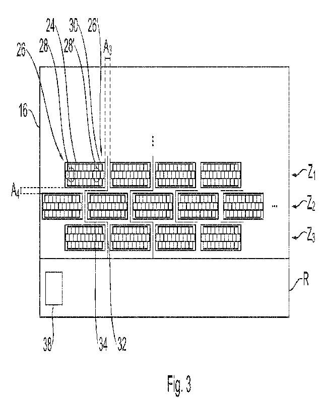
A lidar receiving unit 16 according to the invention is illustrated schemati-
cally in Fig. 3. The lidar receiving unit 16 comprises a multiplicity of
sensor elements
24. The sensor elements are in each case arranged in macro cells 26, 26',
wherein
a macro cell 26, 26' comprises those sensor elements 24 which are together
allo-
cated to an individual emission element 22 of the lidar emitting unit. Two
macro
cells 26, 26' are arranged in a macro cell cluster 30 in each case. The
plurality of
macro cell clusters 30 are arranged in a plurality of rows Zi, Z21 Z3. Routing
channels
32 are arranged between two adjacent macro cell clusters 30 in each case,
which
routing channels cross the rows Zil Z21 Z3 and are constructed to transport
the sig-
nals of the sensor elements 24 to an edge region R of the lidar receiving unit
16.
Two exemplary spot positions 28, 28' are furthermore marked schematically
in the illustration of Fig. 3, which correspond to the positions of allocated
emission
elements of the lidar emitting unit in the array of the lidar receiving unit
16.
CA 03140197 2021-11-30
It is understood that only a detail of the structure of the chip of the lidar
receiving unit 16 is illustrated in Fig. 3, in order to visualize the
arrangement of the
sensor elements 24, routing channels 32, macro cells 26 and macro cell
clusters 30.
The chip extends further upwards and to the side in the illustration.
Preferably, the
number of macro cells corresponds to the number of emission elements of the
lidar emitting unit 18. For a better overview, in each case not all sensor
elements
24 or macro cells 26, 26' and macro cell clusters 30 are provided with
reference
numbers.
As illustrated, the routing channels 32 in the illustrated exemplary embodi-
ment in each case run between adjacent macro cell clusters 30 and transport
the
signals in a direction orthogonal to the course of the rows Z1, Z2, Z3. In the
illus-
trated exemplary embodiment, the routing channels have channel sections 34 in
this case, which run in a region between the rows, parallel to the rows. As a
result,
it becomes possible that the macro cell clusters 30 of a first row are
arranged offset
with respect to the macro cell clusters 30 of a second row, which is adjacent
to the
first row. This has the effect that in the vertical direction, no vertical
blind regions
are created. In this respect, the macro cell clusters 30 are arranged in an
interlace
structure. The sensor elements or spots of the adjacent row are arranged in
the
gaps of a row.
As furthermore shown in the illustrated exemplary embodiment, a distance
A3 between adjacent macro cell clusters 30 of a row is greater than a distance
A4
between adjacent macro cell clusters 30 in adjacent (neighbouring) rows. The
rout-
ing channels 32 run within the distance A3 or between the macro cell clusters.
In
addition, preprocessing elements, preferably transistors, may be arranged be-
tween the rows Z1, Z2, Z3.
Evaluation electronics 38 may be provided in the edge region of the chip of
the lidar receiving unit 16, which are designed to read the sensor elements 24
row-
by-row or to further process the signals of the sensor elements.
11
CA 03140197 2021-11-30
An individual macro cell cluster 30 is illustrated schematically in Fig. 4. In
the
illustrated exemplary embodiment, the macro cell cluster 30 in total comprises
28
sensor elements 24 and two macro cells 26, 26' respectively. In the
illustrated ex-
emplary embodiment, two sensor elements with reduced sensitivity 36, 36' are
arranged between the two macro cells 26, 26' or at the edge of one or both
macro
cells 26, 26'. For example, the sensor elements with reduced sensitivity 36,
36' may
be sensor elements with a metallization on the opening, so that fewer photons
can
be received. The sensor elements with reduced sensitivity 36, 36' may also be
termed aperture SPADs. It is understood that a different number of sensor ele-
ments with reduced sensitivity may also be used.
In the illustration, two exemplary spot positions 28, 28' are marked, which
represent positions of emission elements, which are allocated to the macro
cells
26, 26'. As a whole number multiple of a diameter Ds of the sensor elements is
different from a distance DA between midpoints of allocated emission elements
of
the lidar emitting unit, which are located at the positions P1 and P2, a
balancing
out of alignment errors is achieved. The highest photon density is in each
case re-
ceived at the centre of the spot positions 28, 28' of the emission elements on
the
macro cell cluster. In other words, the reception elements at the centres of
the
spot positions 28, 28' receive the highest photon density in each case. As the
spot
positions 28, 28' cannot be aligned exactly with respect to the array of the
lidar
receiving unit, a distance DA, which corresponds to a whole number multiple of
the
distance Ds, would lead to both spot positions 28, 28' being hit well or
poorly. Due
to the choice according to the invention of the distances Ds and DA, this is
avoided
and a levelling of the errors is achieved in the event of imprecise alignment.
The invention was described and explained comprehensively on the basis of
the drawings and the description. The description and explanation are to be un-
derstood as an example and non-limiting. The invention is not limited to the
em-
bodiments disclosed. Other embodiments or variations will arise for the person
12
CA 03140197 2021-11-30
skilled in the art when using the present invention and during a precise
analysis of
the drawings, the disclosure and the following patent claims.
In the patent claims, the words "comprise" and "with" do not exclude the
presence of further elements or steps. The indefinite article "a" or "an" does
not
exclude the presence of a plurality. An individual element or an individual
unit may
execute the functions of a plurality of the units mentioned in the patent
claims. An
element, a unit, an interface, a device and a system may be implemented
partially
or completely in hard- and/or software. The mere mention of a few measures in
several dependent patent claims is not to be understood to mean that a combina-
tion of these measures cannot likewise be used advantageously. Reference num-
bers in the patent claims are not to be understood as limiting.
13
CA 03140197 2021-11-30
Reference numbers
Lidar measuring device
12 Object
5 14 Vehicle
16 Lidar receiving unit
18 Lidar emitting unit
Control unit
10 22 Emission element
24 Sensor element
26 Macro cell
28 Spot position
15 30 Macro cell cluster
32 Routing channel
34 Channel section
36, 36' Sensor element with reduced sensitivity
14
CA 03140197 2021-11-30