Note: Descriptions are shown in the official language in which they were submitted.
CA 03140616 2021-11-15
WO 2020/236767 PCT/US2020/033505
HIGH TEMPERATURE SINTERING SYSTEMS AND METHODS
CROSS-REFERENCE TO RELATED APPLICATION
[0001] This application claims the benefit of, and priority to, U.S.
Provisional Patent
Application No. 62/849,578, filed on May 17, 2019, U.S. Provisional Patent
Application No.
62/975,483, filed on February 12, 2020, and U.S. Provisional Patent
Application No.
63/022,083, filed on May 8, 2020. The entire contents of the foregoing
applications are
hereby incorporated by reference.
BACKGROUND
Technical Field
[0002] The present disclosure relates to sintering systems and methods, and
more
particularly, to fast high-temperature sintering systems and methods.
Related Art
[0003] Ceramics are widely used in electronics, energy storage, and extreme
environments due to their high thermal, mechanical, and chemical stability.
The sintering of
ceramics is a technology that can be traced back to more than 26,000 years
ago. Conventional
ceramic synthesis often involves two steps: a solid state reaction to form the
ceramic from
precursors, and sintering to form a solid component. Each step requires high-
temperatures
and hours of processing time, which can lead to undesirable, non-uniform grain
growth and
become an obstacle for high throughput discovery of advanced ceramic
materials. The long
sintering time is also a considerable issue in the development of new ceramic-
based solid
state electrolytes (SSEs) that are critical for new batteries with improved
energy efficiency
and safety due to the severe volatility of Li and Na during sintering.
[0004] The process temperature of traditional sintering methods is
typically limited to
about 1200 C due to the limitation of heating elements. With specially
designed graphite
1
CA 03140616 2021-11-15
WO 2020/236767 PCT/US2020/033505
furnaces, the temperature can achieve 2000 C. However, bulk furnaces are
difficult to
control for temperature and temperature distribution, and temperature ramping
and cooling
rates are prolonging. The bulky and sealed equipment are also difficult to
monitor and study
to understand possibilities for improvement, which results in trial-and-error
process with long
iterations that heavily limit materials discovery, especially for ceramics,
glass and metal
materials.
[0005] In this regard, substantial effort has been devoted to the
development of
innovative sintering technologies, such as microwave-assisted sintering, spark
plasma
sintering (SPS), and flash sintering. However, microwave-assisted sintering
fundamentally
depends on the microwave absorption properties of the materials, limiting its
universal
applicability. The SPS technique requires dies to compress the ceramic while
sintering,
which limits product geometries and scalability and is not suitable for
sintering complex 3D
structures due to the applied pressure, and it cannot sinter multiple
specimens at the same
time. A more recently-developed flash sintering method displays a high heating
rate of up to
about 10,000 C/min. However, it typically requires expensive Pt electrodes
and is difficult to
apply to specimens with complex geometry (e.g., 3D structures). In particular,
the specific
flash sintering conditions depend strongly on the electrical characteristics
of the material,
limiting its applicability for high-throughput processing when the material's
properties are
unknown. Thus, there is interest in developing and improving sintering
technology that can
be more universally applied for higher throughput processing.
SUMMARY
[0006] The present disclosure relates to fast high-temperature sintering
systems and
methods. Aspects of the present disclosure provide innovative non-material-
specific,
ultrafast, energy-saving sintering technology that can be applied to different
materials to
2
CA 03140616 2021-11-15
WO 2020/236767 PCT/US2020/033505
enable high-throughput fabrication of bulk ceramics for a broad range of
technological
applications.
[0007] In accordance with aspects of the present disclosure, a method of
fabrication
includes positioning a material at a distance of 0-1 centimeters from a first
conductive carbon
element and at a distance of 0-1 centimeters from a second conductive carbon
element;
heating the first conductive carbon element and the second conductive carbon
element by
electrical current to a temperature between 500 C and 3000 C, inclusive; and
fabricating a
sintered material by heating the material with the heated first conductive
carbon element and
the heated second conductive carbon element for a time period between one
second and one
hour.
[0008] In various embodiments of the method, the method includes initiating
heating of
the first conductive carbon element and the second conductive carbon element,
and the first
conductive carbon element and the second conductive carbon element achieve a
temperature
between 500 C and 3000 C, inclusive, within thirty seconds of initiating the
heating.
[0009] In various embodiments of the method, at least one of the first
conductive carbon
element and the second conductive carbon element are at least partially in
contact with the
material, and the method further includes applying pressure to at least
partially press at least
one of the first conductive carbon element and the second conductive carbon
element against
the material during the heating of the material.
[0010] In various embodiments of the method, the method includes holding
the material
on a conveyor strip, where the first conductive carbon element is positioned
above a portion
of the conveyor strip, and where the second conductive carbon element is
positioned at one
of: a position below a portion of the conveyor strip, or as a portion of the
conveyor strip, and
where positioning the material includes advancing the conveyor strip to convey
the material
between the first conductive carbon element and the second conductive carbon
element.
3
CA 03140616 2021-11-15
WO 2020/236767 PCT/US2020/033505
[0011] In various embodiments of the method, the method includes, at an end
of the time
period, advancing the conveyor strip to remove the sintered material from
between the first
conductive carbon element and the second conductive carbon element while
maintaining the
temperature of the first conductive carbon element and the second conductive
carbon
element.
[0012] In various embodiments of the method, the material is a 3D-printed
material
having a composition and a structure, and the sintered material is a
functional device that
maintains the composition and the structure.
[0013] In various embodiments of the method, the material is a powder
having a plurality
of compositions, and fabricating the sintered material includes causing the
plurality of
compositions to react during the time period.
[0014] In various embodiments of the method, the sintered material is one
of: metals,
alloys, high entropy alloys, refractory metals, refractory alloys, ceramics,
or ion conductors.
[0015] In various embodiments of the method, the sintered material is one
of glass dense
structure or a transparent ceramic dense structure, and fabricating the
sintered material
includes causing the powder to at least partially melt.
[0016] In various embodiments of the method, the material is a multilayer
structure
having at least two layers, wherein the sintered material includes an
interface layer between
the at least two layers, the interface layer having a depth less than 10 um.
[0017] In various embodiments of the method, the material includes at least
two
compositions, where the sintered material is a composite structure that
includes the at least
two compositions, and where the composite structure has an interface layer
between the at
least two compositions, where the interface layer having a depth less than 10
um.
4
CA 03140616 2021-11-15
WO 2020/236767 PCT/US2020/033505
[0018] In various embodiments of the method, the material is identified in
a
computational study, and the method includes analyzing the sintered material
to validate
computations of the computational study.
[0019] In various embodiments of the method, the method includes
positioning a plurality
of additional materials between the first conductive carbon element and the
second
conductive carbon element, and fabricating a plurality of additional sintered
materials by
heating the plurality of additional material with the heated first conductive
carbon element
and the heated second conductive carbon element for the time period, where the
plurality of
additional materials are co-sintered simultaneously with the material.
[0020] In various embodiments of the method, the plurality of additional
materials are
identified in a computational study.
[0021] In accordance with aspects of the present disclosure, a furnace
includes a material,
a first conductive carbon element positioned at a distance of 0-1 centimeters
from the
material, a second conductive carbon element positioned at a distance of 0-1
centimeters from
the material, an electrical source configured to cause the first conductive
carbon element and
the second conductive carbon element to heat by electrical current to a
temperature between
500 C and 3000 C, inclusive, and a controller configured to control the
electrical source to
heat the material with the heated first conductive carbon element and the
heated second
conductive carbon element for a time period between one second and one hour.
[0022] In various embodiments of the furnace, at least one of the first
conductive carbon
element and the second conductive carbon element are at least partially in
contact with the
material, and the furnace includes a pressure mechanism, where the controller
is configured
to control the pressure mechanism to at least partially press at least one of
the first conductive
carbon element and the second conductive carbon element against the material
during the
heating of the material.
CA 03140616 2021-11-15
WO 2020/236767 PCT/US2020/033505
[0023] In various embodiments of the furnace, the furnace includes a
conveyor strip
holding the material, where a portion of the conveyor strip is positioned
between the first
conductive carbon element and the second conductive carbon element, and where
the
controller is configured to control the conveyor strip to convey the material
between the first
conductive carbon element and the second conductive carbon element.
[0024] In accordance with aspects of the present disclosure, a method of
fabrication
includes positioning a conductive carbon element at a distance of at most 1
centimeter from a
material where the material has a larger size than a size of the conductive
carbon element,
heating the conductive carbon element by electrical current to a temperature
between 500 C
and 3000 C, inclusive, and moving the heated conductive carbon element over
the material to
provide a treated material.
[0025] In various embodiments of the method, moving the heated conductive
carbon
element over the material causes annealing of the material. In various
embodiments of the
method, the annealing of the material creates a new surface layer at a surface
of the material.
[0026] In various embodiments of the method, the material includes a thin
film over a
substrate, the method further comprising depositing the thin film onto the
substrate by using
one of: sputtering, chemical vapor deposition, atomic layer deposition, or
physical vapor
deposition.
[0027] In various embodiments of the method, moving the heated conductive
carbon
element over the material causes sintering of the material to provide a
sintered material.
[0028] In various embodiments of the method, the method includes applying a
layer over
the sintered material, and moving the heated conductive carbon element over
the layer to
provide a sintered layer, where the sintered material and the sintered layer
together form a
sintered multilayer structure.
6
CA 03140616 2021-11-15
WO 2020/236767 PCT/US2020/033505
[0029] In various embodiments of the method, the material includes a coated
powder
over a substrate and the sintered material includes a sintered coating over
the substrate.
[0030] In various embodiments of the method, the material is one of: a
printed film of
solid state electrolyte (SSE) precursor or a film of an SSE powder, and the
method includes
dispensing one of an SSE precursor slurry or the SSE powder into a film, where
the sintered
material is a sintered SSE film.
[0031] In various embodiments of the method, the material is a thermal
barrier coating
coated over a metal substrate, where the thermal barrier coating including a
top porous layer
and a bottom dense layer, where the top porous layer has pore sizes between 1-
10,000 nm,
where the sintered material is a sintered thermal barrier coating on the metal
substrate, and
where the top porous layer and the bottom dense layer are one of: co-sintered
in a single
sintering process, or sintered one layer at a time in separate sintering
processes.
[0032] In various embodiments of the method, the material is an
environmental barrier
coating coated over a metal substrate, where the sintered material is a
sintered environmental
barrier coating on the metal substrate.
[0033] In accordance with aspects of the present disclosure, a furnace
includes a material,
a conductive carbon element positioned at a distance of at most 1 centimeter
from the
material where the material has a larger size than a size of the conductive
carbon element, an
electrical source configured to cause the conductive carbon element to heat by
electrical
current to a temperature between 500 C and 3000 C, inclusive, a mechanical arm
configured
to move the heated conductive carbon element over the material to provide a
treated material,
and a controller configured to control the electrical source to heat the
conductive carbon
element and configured to control the mechanical arm to move the heated
conductive carbon
element.
7
CA 03140616 2021-11-15
WO 2020/236767 PCT/US2020/033505
[0034] In accordance with aspects of the present disclosure, a structure
includes a
sintered composite structure having at least two compositions and an interface
layer between
the at least two compositions, where the interface layer has a depth of less
than 10 um.
[0035] In various embodiments of the structure, the at least two
compositions of the
sintered composite structure include one of: metal and carbon nanomaterials,
metal and
ceramics, or alloy and alloy, where the carbon nanomaterials include one of:
nanotubes or
graphene.
[0036] In various embodiments of the structure, each of the at least two
compositions of
the sintered composite structure is a material from the group consisting of:
ceramics, glass,
metals, alloys, carbon, or polymers.
[0037] In various embodiments of the structure, each of the at least two
compositions of
the sintered composite structure is one of: a dense composition or a porous
composition.
[0038] In accordance with aspects of the present disclosure, a structure
includes a
sintered multilayer structure having at least two layers, where a first layer
of the at least two
layers has a different material than a second layer of the at least two
layers.
[0039] In various embodiments of the structure, each of the at least two
layers of the
sintered multilayer structure includes a material from the group consisting
of: ceramics, glass,
metals, alloys, carbon, or polymers.
[0040] In various embodiments of the structure, each of the at least two
layers of the
sintered composite structure is one of: a dense layer or a porous layer.
[0041] In various embodiments of the structure, the first layer of the
sintered multilayer
structure is a porous layer and the second layer of the sintered multilayer
structure is a dense
layer, wherein the dense layer is one of: a single dense layer or at least two
dense sub-layers.
[0042] In various embodiments of the structure, the at least two layers of
the sintered
multilayer structure includes a third layer, wherein the third layer is a
porous layer.
8
CA 03140616 2021-11-15
WO 2020/236767 PCT/US2020/033505
[0043] In various embodiments of the structure, the first layer is a solid
state electrolyte
and the second layer is a different solid state electrolyte, and the sintered
multilayer structure
forms a multifunctional solid state electrolyte.
[0044] In various embodiments of the structure, the at least two layers
includes a third
layer, wherein: the first layer is a solid state electrolyte, the second layer
is an electrode, and
the third layer is an interface layer between the electrode and the solid
state electrolyte, where
the interface layer has a depth less than 10 p.m.
[0045] In various embodiments of the structure, the structure includes a
solid state
battery, where the solid state battery includes the sintered multilayer
structure, and the
sintered multilayer structure is a solid state electrolyte.
[0046] In various embodiments of the structure, the structure includes a
fuel cell, where
the fuel cell includes the sintered multilayer structure, and the sintered
multilayer structure is
a solid state electrolyte.
[0047] In aspects of the present disclosure, a method of fabricating a
thermoelectric
device includes providing a p-type thin film on a substrate, providing a n-
type thin film on
the substrate, positioning at least one conductive carbon element at a
distance of at most 1
centimeter from the p-type thin film and the n-type thin film, heating the at
least one
conductive carbon element by electrical current to a temperature between 500 C
and 3000 C,
inclusive, sintering the p-type thin film and the n-type thin film by heat
from the at least one
heated conductive carbon element, and providing at least one electrode on at
least a portion of
at least one of the sintered p-type thin film or the sintered n-type thin
film.
[0048] In various embodiments of the method, the p-type thin film and the n-
type thin
film are sintered simultaneously.
[0049] In various embodiments of the method, the p-type thin film and the n-
type thin
film are sintered sequentially.
9
CA 03140616 2021-11-15
WO 2020/236767 PCT/US2020/033505
[0050] In aspects of the present disclosure, a piezoelectric device
includes a first
electrode and a second electrode, and a sintered piezoelectric thin film
between the first
electrode and the second electrode.
[0051] Further details and aspects of exemplary embodiments of the present
disclosure
are described in more detail below with reference to the appended figures.
BRIEF DESCRIPTION OF THE DRAWINGS
[0052] The above and other aspects and features of the present disclosure
will become
more apparent in view of the following detailed description when taken in
conjunction with
the accompanying drawings wherein like reference numerals identify similar or
identical
elements and:
[0053] FIG. 1 is a diagram of an exemplary UHS sintering process, in
accordance with
aspects of the present disclosure;
[0054] FIG. 2 is a diagram of an exemplary configuration of heating
elements for the
UHS process, in accordance with aspects of the present disclosure;
[0055] FIG. 3 is a diagram of an exemplary UHS system that includes
applying pressure
to the heating elements, in accordance with aspects of the present disclosure;
[0056] FIG. 4 is a diagram of an exemplary UHS system that includes a
conveyor strip, in
accordance with aspects of the present disclosure;
[0057] FIG. 5 is a diagram of an exemplary USH system that includes a
movable heating
bar for sintering a top layer of a material, in accordance with aspects of the
present
disclosure;
[0058] FIG. 6 is a diagram of an exemplary 3D-printed structures which can
be sintered
using UHS systems and processes, in accordance with aspects of the present
disclosure;
CA 03140616 2021-11-15
WO 2020/236767 PCT/US2020/033505
[0059] FIG. 7 is a diagram of an exemplary operation of applying the UHS
systems and
processes to powders, in accordance with aspects of the present disclosure;
[0060] FIG. 8 is a diagram of exemplary multilayer structures formed by
applying UHS
systems and processes, in accordance with aspects of the present disclosure;
[0061] FIG. 9 is a diagram of an exemplary operation of applying UHS
systems and
processes for co-sintering compositions to form a composite structure, in
accordance with
aspects of the present disclosure;
[0062] FIG. 10 is a diagram of an exemplary operation of applying UHS
systems and
processes to conduct post-treatment for solid materials, in accordance with
aspects of the
present disclosure;
[0063] FIG. 11 is a diagram of an exemplary operation of applying UHS
systems and
processes to treat a surface of a solid material, in accordance with aspects
of the present
disclosure;
[0064] FIG. 12 is a diagram of an exemplary operation of applying UHS
systems and
processes to treat a thin film at the surface of a substrate, in accordance
with aspects of the
present disclosure;
[0065] FIG. 13 is a diagram of an exemplary operation of applying UHS
systems and
processes to co-sinter electrode materials and solid state electrolytes, in
accordance with
aspects of the present disclosure;
[0066] FIG. 14 is a diagram of an exemplary operation of applying UHS
systems and
processes to co-sinter and fabricate solid state batteries, in accordance with
aspects of the
present disclosure;
[0067] FIG. 15 is a diagram of an exemplary operation of applying UHS
systems and
processes to fabricate printed thin film batteries, in accordance with aspects
of the present
disclosure;
11
CA 03140616 2021-11-15
WO 2020/236767 PCT/US2020/033505
[0068] FIG. 16 is a diagram of exemplary multilayer structures formed by
applying UHS
systems and processes for different applications (e.g., batteries and fuel
cells), in accordance
with aspects of the present disclosure;
[0069] FIG. 17 is a diagram of an exemplary thermoelectric device formed by
applying
UHS systems and processes, in accordance with aspects of the present
disclosure;
[0070] FIG. 18 is a diagram of an exemplary piezoelectric device and thin
film formed by
applying UHS systems and processes, in accordance with aspects of the present
disclosure;
[0071] FIG. 19 is a diagram of an exemplary thermal barrier coating or
environmental
barrier coating formed by applying UHS systems and processes, in accordance
with aspects
of the present disclosure;
[0072] FIG. 20 is a diagram of an exemplary process of computation
screening and
fabrication of materials by applying UHS, in accordance with aspects of the
present
disclosure; and
[0073] FIG. 21 is a diagram of an exemplary UHS system for simultaneously
co-sintering
multiple materials, in accordance with aspects of the present disclosure.
DETAILED DESCRIPTION
[0074] The present disclosure relates to fast high-temperature sintering
systems and
methods. Aspects of the present disclosure provide innovative non-material-
specific,
ultrafast, energy-saving sintering technology that can be applied to different
materials to
enable high-throughput fabrication of bulk ceramics for a broad range of
technological
applications. As will be explained below and in connection with the figures,
the present
disclosure provides systems and methods for sintering many types of materials
in a process
that can be as fast as forty-five seconds or less, providing a significant
improvement over
conventional furnace sintering times of more than twenty hours.
12
CA 03140616 2021-11-15
WO 2020/236767 PCT/US2020/033505
[0075] As used herein, and unless otherwise indicated otherwise, the term
"sintering"
refers to a process which forms a solid mass of material by heat and/or
pressure without
completely liquefying the material and can include processes which partially
melt a material
without completely liquefying it. In certain situations, the term "sintering"
may refer to a
process that melts materials, as explained for various situations described
below.
[0076] The sintering process disclosed herein may be referred to as
ultrafast high-
temperature sintering ("UHS") or as high temperature pulse ("HTP") sintering.
The UHS
process features uniform temperature distribution, fast heating rates (e.g.,
2,000-100,000
C/min) and fast cooling rates (e.g., up to about 10,000 C/min), and high
sintering
temperatures (e.g., up to about 3,000 C). The high heating rates and high
temperature of the
heating source enable ultrafast sintering times of less than ten seconds and
overall processing
times of approximately forty-five seconds or less. Additionally, the UHS
process is scalable
and has minimal sample requirements in terms of intrinsic properties and
preparation, thus
providing universal and rapid ceramic synthesis and sintering. UHS enables
rapid
experimental validation for new material predictions from computation to
facilitate materials
discovery. Accordingly, the systems and methods disclosed herein provide a
significant
advance for rapid materials screening and synthesis that could be applied in a
wide range of
fields, including batteries, 3D printed ceramics, and high-entropy ceramics
with vast
compositional space that is otherwise difficult to explore.
[0077] In accordance with aspects of the present disclosure, and as
explained in more
detail later herein, the UHS process directly synthesizes ceramics from oxide
precursors in a
single step, in which the precursor pellet is quickly and uniformly sintered
between two
carbon strips through radiative heating. The short sintering time prevents
volatile evaporation
and undesirable interdiffusion at interfaces (i.e., cross-contamination).
Additionally, the UHS
process is compatible with 3D printing of ceramic precursors, producing novel
structures that
13
CA 03140616 2021-11-15
WO 2020/236767 PCT/US2020/033505
are retained after sintering, in addition to well-defined interfaces between
multilayer ceramic
compounds, with applicability for thin film SSE applications.
[0078] The UHS process for synthesizing ceramics or other solid materials
has the
following attributes. (1) The UHS process can directly synthesize and sinter
precursors into
solid, dense ceramics or glass thin films, reducing sintering time from tens
of hours to less
than ten seconds, which allows fast converging to successful synthesis for
rapid materials
screening. (2) High temperature leads to melted and merged grain boundaries
while
avoiding/mitigating uncontrolled grain growth. Such control results in
outstanding
performance and superior mechanical and electrochemical properties. (3) Short
sintering time
avoids/mitigates Li loss problem of solid state electrolytes (SSEs) during
synthesis and
avoids/mitigates side reactions, and results in multilayer structures without
crossover
diffusion. (4) The UHS process is a universal process for a wide range of
ceramics, glass, and
other solid materials. These attributes demonstrate the uniqueness of the UHS
process as a
physicochemical process for discovering ceramics, glass, and other solid
materials.
[0079] Portions of the present disclosure refer to U.S. Provisional Patent
Application No.
62/849,578, filed on May 17, 2019, which has been incorporated by reference in
its entirety,
and which may be referred to herein as "Supplement."
[0080] Portions of the present disclosure refer to U.S. Provisional Patent
Application No.
63/022,083, filed on April 30, 2020, which has been incorporated by reference
in its entirety,
and which may be referred to herein as "Supplement B."
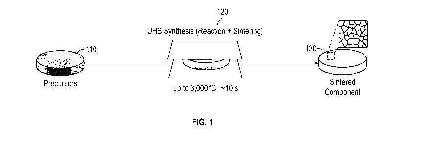
[0081] Referring now to FIG. 1, there is shown an exemplary UHS process for
sintering
material precursors. The precursors 110 are directly sintered into a dense
ceramic pellet 130
in approximately ten seconds in one step at a high sintering temperature of up
to about 3,000
C. In contrast, a conventional ceramic synthesis is a two-step process that
involves a 5-10
hour solid-state reaction step at 800-1,000 C for forming the ceramic phase
from precursors,
14
CA 03140616 2021-11-15
WO 2020/236767 PCT/US2020/033505
followed by hours-long sintering at typically 1,000-1,600 C to form dense
components. In
general, the UHS sintering process is approximately 2-4 orders of magnitude
faster than
conventional sintering methods (Supplement, Table 51).
[0082] In FIG. 1, an exemplary embodiment of the UHS process is shown, in
which the
precursor pellet 110 is directly "sandwiched" between two blanket Joule-
heating carbon
strips 120 that can rapidly heat the sample pellet 110 through radiation
and/or conduction to
form a uniform high-temperature environment for quick synthesis (solid-state
reaction) and
reactive sintering. In an inert atmosphere, the carbon heating elements 120
can provide a
temperature higher than 3,000 C (Supplement, Fig. 51), which is sufficient
for synthesizing
and sintering virtually any ceramic material, though most do not require a
temperature this
high. In various embodiments of the UHS process, the heating elements 120 can
ramp up
from room temperature to the sintering temperature in approximately thirty
seconds or less,
followed by approximately ten seconds of sintering time and then rapid cooling
of
approximately five seconds. The short processing duration results in the
ability to achieve
excellent compositional control of ceramics which contain volatile components
(e.g., Li in
solid-state electrolytes for Li ion batteries), as well as the ability to
prevent uncontrolled grain
growth for outstanding material performance.
[0083] The temperature of the heating elements 120 is tunable to different
ramp rates,
including heating rates of about 100 C/min to about 20,000 C/min, and
cooling rates of
about 100 C/min to about 10,000 C/min. The achievable temperature of the
heating
elements 120 can range from about 500 C up to about 3,500 C. At maximum
sintering
temperature, the UHS process enables direct sintering of ceramics, glass, or
other solid
materials from precursors 110 to dense pellets 130 in less than ten seconds.
Due to the rapid
sintering speed, evaporation of volatile materials and potential cross-
contamination can be
significantly minimized, which enables co-sintering of multiple materials in
one step.
CA 03140616 2021-11-15
WO 2020/236767 PCT/US2020/033505
[0084] In contrast, the conventional ceramic synthesis process involves
multiple steps
and long time. The precursors are first calcinated at about 800-1000 C for 5-
10 hours to form
ceramic phase. Then the materials are re-grinded to ceramic power and pressed
to pellets,
which are sintered at about 1000-1200 C for another 10-30 hours to form dense
pellets. If the
ceramics contain volatile components, additional ceramic powder beds with
excess volatile
components are necessary to compensate the evaporation at high temperature
during the long-
time sintering. The long sintering time can lead to uncontrollable grain
growth and
nonuniform size distribution (Supplement, Figure B 1A), while the relative low
sintering
temperature can result in the weak-bonded grain boundaries, which will
decrease the
mechanical strength and affect the uniformity of the ceramic properties.
[0085] When the space between the heating element 120 and the material 110
is small, or
the material 110 directly contacts the heating element 120, the temperature
ramp rate of the
sample 110 can be much faster, and the temperature distribution is more
uniform than
conventional furnaces. The short sintering time of the UHS process enables
control of the
grain growth, while the high sinter temperature ensures the excellent welding
of the grain
boundaries, which leads to uniformly distributed and well-merged small grains
for UHS
sintered ceramics (Supplement, Figure BM). Various embodiments of UHS systems
and
processes are described below in connection with the figures.
[0086] FIG. 2 is a diagram of an exemplary configuration of heating
elements for the
UHS process. One heating element 210 is positioned on one side of the material
230 and a
second heating element 220 is position on the other side of the material 230.
The heating
elements 210, 220 can be wholly or partially in contact with the material 230
or can be
positioned 1 cm or less away from the material 230. The material 230 can be
supported in
various ways, such as by a tray in a furnace used for the UHS process, among
others. In
various embodiments, the heating elements 210, 220 are positioned such that
they are
16
CA 03140616 2021-11-15
WO 2020/236767 PCT/US2020/033505
substantially parallel to each other. In various embodiments, the heating
elements 210, 220
are positioned such that they are substantially parallel to the material 230
surface closest to
the heating element. Positioning the heating elements 210, 220 closer to the
material 230
will cause the material 230 to heat at a faster heating rate. Even at a
distance of about 1 cm,
the heating elements 210. 220 can be capable of heating the materials 230 at a
sufficient
heating rate to complete the sintering process in a matter of seconds, such as
10 seconds. In
various embodiments, the material 230 can be positioned on the bottom heating
element
220, and the top heating element 210 can be positioned 1 cm or less away from
the material
230. When the top heating element 210 and the bottom heating element 220 are
different
distances away from the material 220, the heating elements 210, 220 may be
heated at
different heating rates or may achieve different temperatures based on the
different
distances. For example, when the material 230 is positioned on the bottom
heating element
220, the bottom heating element 220 may be heated to a lower temperature than
the top
heating element.
[0087] In various embodiments, the heating elements 210, 220 can be made of
conductive carbon materials, such as carbon papers, carbon felts, carbon
clothes, graphite
papers, graphite felts, graphite clothes, graphite films, or graphite plates.
In various
embodiments, other conductive materials or composites can be used for the
heating
elements. The heating elements 210, 220 can be sized based on sizes of the
materials to be
sintered and to meet manufacturing needs. When the heating elements 210, 220
are made of
conductive materials, the heating elements 210, 220 can be heated by an
electrical source
(not shown) passing electrical current through the conductive materials of the
heating
elements 210, 220. The amount of current through the conductive material of
the heating
elements 210, 220 corresponds to the heating rate, such that the heating rate
and electrical
source can be controlled by a controller (not shown) by providing a desired
amount of
17
CA 03140616 2021-11-15
WO 2020/236767 PCT/US2020/033505
current through the conductive materials of the heating elements 210, 220.
Heating profiles
are described in more detail in Supplement with respect to particular
materials. It is
sufficient to note here that current should be passed through the heating
elements in the
same direction to cause the heating elements 210, 220 to apply heat to the
material 230 in
the same direction. In various embodiments, the heating elements 210, 220 can
have
approximately a width of 2 cm and a length of 10 cm. Other shapes and sizes
for the heating
elements are contemplated to be within the scope of the present disclosure.
[0088] The heating environment can be a vacuum or can include one or more
of inert
gas, Ar, N2, hydrogen, carbon dioxide, oxygen, air, and/or other gases. The
heating
environment can be varied based on the type of material and type of heating
elements.
[0089] FIG. 3 is a diagram of a UHS system that includes applying pressure
to the
heating elements. The heating elements 310, 320 and heating environment may be
the same
as those described in connection with FIG. 2. The heating elements 310, 320
are placed in
contact with the material 330, and pressure may be applied to the heating
elements 310, 320
by various mechanisms 340, 350, such as hydraulic plates, robotic/mechanical
arms, or other
mechanical pressure applicators. In various embodiments, the heating elements
310, 320 can
be secured to the pressure applicators 340, 350. The application of pressure
can cause the
sintered materials 360 to have higher density. In various embodiments, the
amount of
pressure exerted can be electronically controlled by a controller (not shown)
based on desired
density and/or based on other parameters.
[0090] FIG. 4 is a diagram of a UHS system that includes a conveyor strip.
The heating
elements 410, 420 and heating environment may be the same as those described
in
connection with FIG. 2. The materials 430 can be placed on the conveyor strip
440, and the
heating elements 410, 420 may be positioned less than 1 cm away from the
materials 430 to
be sintered. The conveyor strip 440 can be made of a heat-resistant material
that can
18
CA 03140616 2021-11-15
WO 2020/236767 PCT/US2020/033505
withstand the high temperatures of the heating elements 410, 420 and that can
quickly heat up
and cool down. In embodiments where the lower heating element 420 is below the
conveyor
strip 440, the lower heating element 420 may be heated to a higher temperature
than the
upper heating element 410 to provide more uniform sintering. In various
embodiments, the
lower heating element 420 can be incorporated into the conveyor strip 440 and
form part of
the conveyor strip 440, such that the material 430 to be sintered can be
placed in contact with
a heating element 420 that is directly on the conveyor strip 440. In
embodiments where the
material 430 is in contact with the lower heating element 420, the lower
heating element 420
may be heated to a lower temperature than the top heating element 410, to
provide more
uniform sintering. Because the sintering time can be very short (e.g., ten
seconds), the
conveyor strip 440 can operate continuously for rapid sintering and
manufacturing high
throughput. In various embodiments, the heating elements 410 may be smaller in
size than
the size of the material 430, such that the entirety of the material 430 is
sintered by the
conveyor strip 440 advancing the material 430.
[0091] Not every components of a conveyor system is shown or described, as
persons
skilled in the art will recognize and understand such components. For example,
a conveyor
system that moves the conveyor strip can include rollers, motors, and
controllers, among
other components. A controller (not shown) can control an electrical source to
heat the
heating elements and can control the conveyor system to advance the material.
Additionally,
the conveyor strip can be used for other purposes, such as post-treatment of
solid materials
which will be described in connection with FIG. 10 and 11. For such other
purposes, the
heating elements may be positioned up to several inches away from the
materials and the roll
speed of the conveyor strip can be adjustable so that the materials can be
heated for a suitable
duration, such as from 1 second to 1 hour, or another time duration.
19
CA 03140616 2021-11-15
WO 2020/236767 PCT/US2020/033505
[0092] The embodiments of FIGS. 1-4 are exemplary and variations are
contemplated to
be within the scope of the present disclosure. For example, in various
embodiments, only one
heating element may be used rather than both heating element being used. In
various
embodiments, rather than having two heating elements, the systems and
processes of FIGS.
1-4 may have only one heating element. The time to heat the heating elements
to a target
temperature can vary. The amount of time to sinter a material can vary and can
be between
one second and one hour.
[0093] FIG. 5 is a diagram of a USH system that includes a movable heating
bar for
sintering a top layer of a material. The heating bar 530 can include a heating
element made
from the materials described in connection with the heating element of FIG. 2.
The heating
element can be secured to a mechanical arm or other mechanical mechanism (not
shown) that
can move the heating element across the surface of a material 510. As
described above, the
heating element can be positioned approximately 1 cm or less away from the
surface of the
material 510. The heating bar 530 can be scanned across the surface of the
material 510 to
sinter a top layer 540 of the material, such as a coating layer 510 above a
substrate 520, thin
films, or other multilayer structures. Not every component of a heating bar
system is shown
or described, as persons skilled in the art will recognize and understand such
components. For
example, a heating bar system that moves the heating bar can include motors,
sensors, and
controllers, among other components. The controller can control an electrical
source to heat
the heating bar and can control the mechanical arm or other mechanism to move
the heating
bar across the surface of the material.
[0094] In various embodiments, the heating bar 530 UHS system can be
applied to a
coating 510 process involving steel powder. As an example, in the coating
process, a steel
powder (e.g., powder mixture of elemental metals, i.e. Fe, Mn, Ni, Cr, 1-5 um
powder size)
with 3-5 wt% polymer binder can be dispersed in ethanol to make a slurry. The
viscosity of
CA 03140616 2021-11-15
WO 2020/236767 PCT/US2020/033505
the slurry can be controlled by tuning the concentration of the metal powders
and polymer
binder for different coating techniques, including spray coating and doctor
blade. The powder
slurry can then deposited on a steel substrate or the pipe wall with a wet
thickness of ¨5 mm.
After the coating layer dries in air, a carbon heating bar with a temperature
of ¨ 1500 C can
be closely run over the coating layer to sinter the coating into a dense steel
layer. After the
UHS sintering process, the area of the coating layer close to the carbon
heating bar was
sintered into dense and shiny steel in about five seconds. Cross-sectional SEM
image show
that the sintered steel is about 1 mm thick, dense, and has a tight binding
with the steel
substrate (Supplement B).
[0095] Accordingly, various systems for performing the UHS process are
described
above. The following paragraphs will describe applications of the UHS process
for various
structures and uses.
[0096] FIG. 6 is a diagram of 3D-printed structures which can be sintered
using UHS
systems and process, including complex 3D-printed structures 610, ordered 3D-
printed
structures 620, porous 3D-printed structures 630, and texture-like porous 3D-
printed
structures 640. The composition of the 3D-printed structures 610, 620, 630,
640 can include
various solid materials, including ceramics, glass, metals, alloys, carbons,
polymers, and
other solid state materials and their composites. The geometries of the 3D-
printed structures
610, 620, 630, 640 can be any shape. The structures can be formed by 3D
printing methods
that include extrusion, UV-aided solidification, ink jet, or any other
printing techniques. In
various embodiments, the 3D-printed structures 610, 620, 630, 640 can be
functional devices
having different compositions and complex structures.
[0097] Uniform temperature distribution of the UHS systems and processes
enable the
structures to shrink uniformly in every direction, which maintains the form of
the printed
structures 612, 622, 632, 642 after UHS sintering. Thus, the UHS process
maintains the
21
CA 03140616 2021-11-15
WO 2020/236767 PCT/US2020/033505
composition and structure of the devices after sintering 612, 622, 632, 642 to
achieve
functional devices. In various embodiments, the sintered 3D-printed structures
612, 622, 632,
642 can maintain excellent mechanical, electrical, optical, thermal, acoustic,
magnetic, and
other physical and chemical properties, after undergoing the UHS process. In
various
embodiments, the 3D-printed structure can be used as support materials for
other
applications, such as catalysis. In various embodiments, the UHS systems and
processes can
be used to sinter complex porous 630 or textile-like porous structures 640.
The porous
structures 630 can be 3D or 2D structures, which can have various morphologies
and can be
random or ordered structures. The porosity and pore size of the porous
structures 630 and
vary. In various embodiments, 2D textile-like structures 642 that have gone
through the UHS
process can possess flexibility. In accordance with aspects of the present
disclosure, the UHS
systems and processes disclosed herein (e.g., FIGS. 1-5, 10-15, 21) can be
used to sinter all
such three-dimensional and/or porous structures, whether they are formed by 3D-
printing or
by other ways. The illustrated three-dimensional structures are exemplary and
do not limit the
scope of the present disclosure. The disclosed UHS systems and processes are
generally
applicable to all three-dimensional structures.
[0098] FIG. 7 is a diagram of applying the UHS systems and processes to
powders. The
top portion of FIG. 7 shows an example of reactive sintering in the UHS
process, where the
precursor powders 710 react and sinter into a dense bulk 720. Compositions A,
B, C and D
can be elementary powders or oxide precursors 710. When the powders are
precursor
powders 710, the precursor powders rapidly react and sinter into dense bulk
sample 720 in
one step during the UHS process. For example, in FIG. 7, the precursor powders
A, B, C, and
D 710 react during UHS sintering to form resulting bulk material E 720. The
bottom portion
of FIG. 7 shows an example of direct sintering in the UHS process, where the
powders 730
directly sinter into dense bulk 720. In the bottom portion, the powders 730
can be composite
22
CA 03140616 2021-11-15
WO 2020/236767 PCT/US2020/033505
powders 730, which form the composite without reaction between them. When the
powders
730 are synthesized/composite powders 730 of the resulting bulk material 720,
there is no
reaction among the powders 730 during the UHS sintering process. With regard
to powders,
the sintering temperature can be tuned so the powders partially or fully melt
to form a dense
structure. Thus, in the situation of sintering powders, the term "sintering"
permits the
powders to fully melt.
[0099] In aspects of the present disclosure, the UHS systems and processes
disclosed
herein (e.g., FIGS. 1-5, 10-15, 21) can be applied to rapidly sinter metals
and alloys directly
from powders. Due to the ultra-high temperature of UHS, the UHS process can
rapidly sinter
metals and alloys directly from powders. The powders for alloy sintering can
be a mixture of
elemental powders or can be pre-alloyed powders with same composition the
resulting bulk
material. The metal and alloys can be sintered in various types of UHS
systems, including the
UHS systems shown in FIGS. 1-5. Table 1 below provides non-limiting examples
of
compositions that can be sintered by UHS process. Other compositions not shown
in Table 1
can also be sintered by the UHS process.
[0100] Table 1
Metals W, Fe, Cu, Mn, Ni, Al, Zn, Ti, Mg, Cr, Co, Ta,V, Nb,
Mo, Au,
Ag, Pt, Pd, Sn, Zr, and other metals.
Alloys and metallic Fe-based, Cu-based, Ti-based, Ni-based, Al-based, Mg-
based,
glasses Zr-based, and other alloys and metallic glasses.
High entropy alloys FeCoNiCrMn, TiZrVNbTa, Coi.5CrFeNi1.5Ti,
Alo.2Coi.5CrFeNii.5Ti, AlCoCrFeNi, Cuo.5NiAlCoCrFeSi,
CoCrFeNiCu, CoCrFeNiMn, CoCrFeNiV, MoNbTaVW,
MoNbTaW, AlBxMnNiTi, AlCoxCrCuo.5FeNi, AlxCrCuFeMnNi,
CoCuFeMnNi, AlxCo.2CuFeMnNi, MoTiVFeNiZrCoCr,
ZrTiCuNiBe, PdNiCuP, LaAlNiCu, and CuZrAlY, NbMoTaW,
VNbMoTaW, CoCrFeNiCuAlo.5, VCuFeCoNi, Alo.5CrFeCoNi,
Ti2CrCuFeCoNi, AlTiVYZr, ZrTiVCuNiBe, CrFeCoNiAlCuo.25,
Al3CoCrCuFeNi, NixCoo.6Feo.2-CrySizAlTio.2, BeCoMgTi,
BeCoMgTiZn, CuNiCoZnAlTi, AlCoCrFeNiNbx, BiFeCoNiMn,
CoCrCuFeNiTix, AlCoCrFeNiTix, TaNbHfZrTi, TaNbMoW,
23
CA 03140616 2021-11-15
WO 2020/236767 PCT/US2020/033505
TaNbVMoW, and CrCoCuFeNiAlo.5, NbCrMoo.5Ta0.5TiZr,
NbCrMoo.5Ta0.5TiZr, Tio.8CoCrCuFeNi, NbTiAlVTaLax,
CoCrFeNiCu, and CoCrFeNiAl, TixCoCrCuFeNi, (Ti, Zr, Hf)¨
(Ni, Cu)¨Al, (Fe, Co, Ni)¨(Zr, Hf, Nb, Ta, Mo, W)¨B,
Cuo.5NiAlCoCrFeSi, SrCaYbMgZn,
Zn2oCa2oSr2oYb2o(Lio.55Mgo.45)20, Fe64Moi4C15B6Eri,
Zr4iTii4Cui2.5Ni1oBe22.5, Mg65Cu25Y9Gdi, Pr6oAlioNiloCu2o,
Ce62AlioCu2oCo3Ni5, (Ti33Zr33Hf33)50(Ni5oCu50)40A110,
(Ti25Zr25Hf25Nb25)70(Ni5oCu5o)20A110, (Ti33Zr33Hf33)70(Ni33
Cu33Ag33)20Alio, Ni¨Al¨Cu¨Co¨Ti¨V¨Zn¨Zr, TiZrHfTaNb,
PdPtNiCuP, and other alloy compositions
Ultrahigh-temperature Ni superalloy, Nb-Si Alloys, Mo-Si-B Alloys, IrRhNbNi,
alloys PtAlTa, and other high-temperature alloys.
Intermetallics Zr5Si3, Ti5Si3, MoSi2, TiSi2, NiAl, NiTi, Cu3Sn,
MgCu2, Ag3Sn,
Cu3Sn, FeCo, MgZn2, MgNi2, and other intermetallics.
[0101] In various embodiments, metals and alloys can be sintered in the
form of special
structures, such as 3D-printed structures as described above in connection
with FIG. 6. In
various embodiments, the UHS process can be applied to metal coatings in a
layer-by-layer
printing and sintering process that forms bilayer or multilayer structures,
which is described
below in connection with FIG. 8. For example, the UHS process can sinter a
BMG/crystal
bilayer or multilayer structures. In various embodiments, the UHS process can
rapidly sinter
a wide range of metal and alloys, including Al, Ti, Cu, Fe, refractory metals,
refractory
alloys, and silicide alloys, which can all be directly sintered from the
mixture of the elemental
powders. The sintering temperature of these metal and alloys varies from about
1000 C to
about 3000 C. Besides single-composition pellets, the UHS process can be
applied to co-
sinter multi-materials, such as a Cu/Fe bilayer pellet.
[0102] In aspects of the present disclosure, the USH systems and processes
disclosed
herein (e.g., FIGS. 1-5, 10-15, 21) can be applied to sinter ceramics directly
from powders.
The ceramics can be sintered in various types of UHS systems, including the
UHS systems
24
CA 03140616 2021-11-15
WO 2020/236767 PCT/US2020/033505
shown in FIGS. 1-5. Table 2 below provides a non-limiting list of ceramic
compositions that
can be sintered by UHS process.
[0103] Table 2
Piezoelectric and PZT,PMNT (Pb(Mg1/3Nb2/3)03-PbTiO3),
ferro el ectri c PZNT(Pb(Zn1/31/3Nb2/3)03-PbTiO3)PbTiO3,
ceramics KNN(K1/2Na1/2Nb03), BaTiO3(A=Ca, B=Zr, Sr), BZT-xBCT((1-
x)Ba(Zr0.2Ti0.8)03-x(Ba0.7Ca0.3)TiO3), ZnO, and other
piezo/ferroelectric ceramics
Ionic conductor La2Mo209, LaGa03, Ba2In205, YSZ, LaA103, garnet, A1203,
Li ion
and their thin conductors, Na ion conductors, Mg ion conductors, Al ion
films conductors, Ag ion conductors, H ion conductors, 0 ion
conductors,
and other ion conductors.
Ultra-High HfC, TaC, ZrC, NbC, TiC, WC, VC, ThC, RN, TaN, TiN, ThN,
Temperature ZrN, TiCN, TiC, TiN, Mg0-Be0-A1203, ZrB2, A1203, BN, VB2,
Ceramics TiB2, Hf132, B4C, and other ultrahigh temperature
ceramics.
[0104] In various embodiments, the ceramics can also be sintered in the
form of special
structures, such as 3D-printed structures as described above in connection
with FIG. 6. In
various embodiments, the UHS process can be applied to sinter ceramics in a
layer-by-layer
printing and sintering process that forms thin films, bilayer, or multilayer
structures, which is
described below in connection with FIGS. 8 and 12. For example, multiple thin
film ion
conductors and piezoelectric ceramics can be sintered by the UHS process.
[0105] In aspects of the present disclosure, the UHS systems and processes
disclosed
herein (e.g., FIGS. 1-5, 10-15, 21) can be applied to sinter glass or
transparent ceramics
directly from powders. The powders for glass or transparent ceramics can be a
mixture of
precursor powders or can be pre-synthesized powders having the same
composition as the
resulting bulk material. The glass or transparent ceramics can be sintered in
various types of
UHS systems, including the UHS systems shown in FIGS. 1-5. Table 3 below
provides a
non-limiting list of glass or transparent ceramics compositions that can be
sintered by the
UHS process.
CA 03140616 2021-11-15
WO 2020/236767 PCT/US2020/033505
[0106] Table 3
Glass silicate glass, soda-lime glass, borosilicate glass, lead
glass,
aluminosilicate, A1203-Si203, A1203-Si203-B203, P205, Ge02,
As205, Li20-A1203-Si02, Mg0-A1203 -Si02, Na20-A1203 -Si02,
Zn0-A1203 -Si02, Ba0-Ti02-A1203 -Si02,
Ba0-Ti02-Sr0-
A1203 -Si02, Mg0-Ca0-Si02-P205, Fe203 -Ca0. Si02-B203 -
P205, Na20-Ca0-A1203-Si02, Na20-Ca0-B203-Si02, Na20-
Ca0-A1203-B203-Si02, Na20-Ca0-Si02, and other glass
materials or their composites.
Glass
(energy Multi-layer glass: glass-TC0-(a-Si)-TCO-glass; glass-TC0-(a-Si)-
efficiency) Al-glass (Transparent conducting oxide is called as
"TCO")
BaTiO3 (BT) and PbTiO3 (PT) doped glass
BaTiO3-V205-B203
Si02-ZnO
Si02-TiO2
V02-Si02-Ti02
Glass foam: glass-carbon composite
Transparent Y203, Y3A15012, MgA1204, MgF2, ZnS, ZnSe, A123027N5,
A1203
ceramics Tb3A15012, Tm3A15012, Lu203, Sc203, A2B207, CaF2, SrF2,
BaF2,
CsI, ZnSe, Sr5(PO4)3F, Lu203, Lu3A15012, Mg0, Y-Zr02, YAG,
YSZ, and other transparent ceramics or their composites.
[0107] In various embodiments, the glass or transparent ceramics can also
be sintered in
the form of special structures, such as 3D-printed structures as described
above in connection
with FIG. 6. In various embodiments, the UHS process can be applied to sinter
glass or
transparent ceramics in a layer-by-layer printing and sintering process that
forms thin films,
bilayer, or multilayer structures, which is described below in connection with
FIGS. 8 and 12.
[0108] In aspects of the present disclosure, the UHS systems and processes
disclosed
herein (e.g., FIGS. 1-5, 10-15, 21) can be applied to sinter borides,
carbides, and nitrides
directly from powders. The powders for borides, carbides, and nitrides can be
a mixture of
precursor powders or can be pre-synthesized powders having the same
composition as the
resulting bulk material. The borides, carbides, and nitrides can be sintered
in various types of
UHS systems, including the UHS systems shown in FIGS. 1-5. Table 4 below
provides a
26
CA 03140616 2021-11-15
WO 2020/236767
PCT/US2020/033505
non-limiting list of borides, carbides, and nitrides compositions that can be
sintered by the
UHS process.
[0109] Table 4
Ultra-High HfC,
TaC, ZrC, NbC, TiC, WC, VC, ThC, RN, TaN, TiN, ThN,
Temperature ZrN,
TiCN, TiC, TiN, MgO-Be0-A1203, ZrB2, VB2, TiB2, HfB2,
Ceramics B4C,
and other composties or high entropy ultrahigh temperature
ceramics.
Super hard Borides, carbides, nitrides, and other super hard
materials.
materials Examples: HfC, TaC, ZrC, NbC, TiC, WC, VC, ThC, HfN, TaN,
TiN, ThN, ZrN, TiCN, TiC, TiN, VB2, TiB2, HfB2, WC-Co, 13-SiC,
ZrC, ZrB, ZrB2, WB4, MnB4, ReB2,B4C, (AlCrNbSiTiV)N, and
other composties or high entropy super hard materials.
[0110] In various embodiments, the borides, carbides, and nitrides can also
be sintered in
the form of special structures, such as 3D-printed structures as described
above in connection
with FIG. 6. In various embodiments, the UHS process can be applied to sinter
borides,
carbides, and nitrides in a layer-by-layer printing and sintering process that
forms thin films,
bilayer, or multilayer structures, which is described below in connection with
FIGS. 8 and 12.
[0111] FIG. 8 is a diagram of exemplary bilayer or multilayer structures
(bilayer being
one instance of multilayer) formed by applying UHS systems and processes
disclosed herein
(e.g., FIGS. 1-5, 10-15, 21). A bilayer structure can have a first layer 810
and a second layer
820. A multilayer structure as illustrated has layers 820, 822, 824, and 826,
and so on. The
composition of the layers 810-826 can be any solid materials, including
ceramics, glass,
metals, alloys, carbons, polymers, and/or other solid state materials. The
layers of the bilayer
or multilayer structures 810-826 can be dense or porous. The UHS systems and
processes
described herein (e.g., FIGS. 1-5, 10-15, 21) can be applied to a bilayer
structure where one
of the layers 810 is a porous structure and the other layer 812 is a dense
layer (or vice versa),
thereby forming a porous-dense bilayer. The porous layer 810 can be
infiltrated with
27
CA 03140616 2021-11-15
WO 2020/236767 PCT/US2020/033505
electrode materials for batteries and fuel cell applications. The UHS systems
and processes
can also be applied to any multilayer structure, such as a porous-dense-porous
multilayer
structure for solid state battery, flow battery, and/or fuel cell
applications. Due to the short
sintering time of UHS, the composition of multilayer structures will maintain
without cross
reaction or diffusion.
[0112] In various embodiments, the bilayer or multilayer structures can be
ion
conductors/solid state electrolytes (SSEs). By developing bilayer ceramics as
solid state
electrolytes, the advantages of different electrolytes can be combined to form
multifunctional
SSEs with superior performance in solid state batteries. For example, garnet
can act as
negative side for stable interface with Li metal, and another layer having
good interface with
cathode can be on the positive side. Other bilayer or multilayer thin films
(e.g., three or more
layers) can also be SSEs, and other bilayer and multilayer structure materials
are also
contemplated to be within the scope of the present disclosure.
[0113] In various embodiments, the UHS process can be used to sinter metal
and alloy
bilayers and multilayers. The composition of each layer 810-826 can be any
metals, alloys,
and the bulk metal glasses (BMG). The composition of the high temperature
sintered metals,
alloys, and BMG can be any metals, alloys, metallic glass, intermetallics, and
other metals
and alloys and their composites. The UHS process enables BMG and crystal
compositions to
be successfully co-sintered to form bilayer or multilayer structures, which
combine both
mechanical advantages of BMGs and crystals. Due to the short sintering time,
the diffusion
between the layers is very small/minimized (such as less than 10 p.m) so that
each layer can
maintains the original structure. As an example, Fe-based BMG/crystal bilayer
can be co-
sintered using the UHS process. XRD patterns show pure crystal and glass
phases of each
layer (Supplement B), indicating no obvious side reactions between layers. The
bilayer
design can also be extended to other metal systems. To further improve the
mechanical
28
CA 03140616 2021-11-15
WO 2020/236767 PCT/US2020/033505
properties, some crystal phases can be added to the BMG layer to increase the
ductility
(Supplement B). In this case, the BMG compositions with low glass form ability
can be used
to in situ create some crystal phase in BMG layer. Due to the fast sintering
rate, other crystal
phase can also be added to the BMG layer without cross diffusion.
[0114] FIG. 9 is a diagram of applying UHS systems and processes disclosed
herein (e.g.,
FIGS. 1-5, 10-15, 21) for co-sintering compositions to form a composite
structure. In the left
side of FIG. 9, the composites have a mixture 912 and other structures 910. In
the right side
of FIG. 9, the composites have a core-shell 922 and other structures 920. As
used herein the
term "co-sintering" can refer to applying UHS to sinter multiple compositions
to form a
composite structure. Due to the short sintering time of UHS, the composition
of composite
structures will maintain without/with minimal cross reaction or diffusion
(e.g., less than 10
[tm). The compositions 910-922 of a composite structure can be a combination
of any solid
materials, including ceramics, glass, metals, alloys, carbons, polymers,
and/or other solid
state materials.
[0115] As an example, composite SSEs can make use of advantages of
different
compositions to achieve superior SSEs. By introducing the melting glass state,
composite
SSEs can be sintered at lower temperature and form denser structure. As an
example, a glass-
ceramic composite SSE can be sintered by adding Li3PO4 in LLZTO garnet, where
Li3PO4
can melt at high temperature and weld with LLZTO particles to form a dense
composite
pellet. EDS mapping indicates no obvious cross-doping (Supplement, Figure
B20), and the
XRD pattern confirms no secondary phases or side reactions (Supplement, Figure
B20A). In
contrast, severe side reactions occur between Li3PO4 and LLZTO during one hour
sintering at
1200 C (Supplement, Figure B21 B-D). Therefore, the UHS process enables new
structure
designs for ceramics and glass materials due to the ultra-fast sintering
speed. The UHS
process of FIG. 9 can be applied to sintering other composite structures
having of two or
29
CA 03140616 2021-11-15
WO 2020/236767 PCT/US2020/033505
more compositions. The composition of the composite contents 910-922 can be
ceramics,
glasses, metals, alloys, carbons, polymers, and other solid state materials.
The structure of the
composite can be a mixture of multiple phases (as shown in the left side of
FIG. 9), or can be
a core-shell (as shown in right side of FIG. 9), or can be other structures.
[0116] FIG. 10 is a diagram of applying UHS systems and processes to
conduct post-
treatment for solid materials. The solid materials 1010 can be pre-synthesized
or can be
formed by other sintering techniques. The UHS systems and processes disclosed
herein (e.g.,
FIG. 1-5) can then be applied to the solid materials 1010 as a post-treatment.
For example,
the heating element 1010 may be positioned 1 mm to several inches away from
the materials
1010. The UHS post-treatment can cause the treated solids 1010 to experience
structure,
composition, crystallinity, morphology, surface, or other changes. The treated
solid materials
1030 can have excellent mechanical, electrical, ionic, optical, thermal,
acoustic, magnetic,
and/or other physical and/or chemical properties. In various embodiments, the
solid materials
can be glass or other optical materials with excellent UV-Vis-IR properties or
other optical
properties. The composition of the solid material 1010 can be any solid
materials, including
ceramics, glasses, metals, alloys, carbons, polymers, and other solid state
materials and their
composites.
[0117] FIG. 11 is a diagram of applying UHS systems and processes disclosed
herein
(e.g., FIGS. 1-5) to treat a surface of a solid material 1110. The solid
material 1110 can be
ceramics, glass, metals, alloys, carbons, polymers, and/or other solid state
materials. In
various embodiments, the solid material 1110 can be in direct contact with the
heating
element 1120 or can be 1 mm to several inches away from the heating element
1120. In
various embodiments, the UHS process and the high temperature can quickly heat
the sample
surface to form a new surface layer 1130, which has new structure, morphology,
composition, or other property changes. The UHS treating temperature and time
can be
CA 03140616 2021-11-15
WO 2020/236767 PCT/US2020/033505
adjusted to achieve desired thickness or properties of the surface layer 1130.
Thus, the UHS
process can cause a change in just the new surface layer 1130 of the solid
material without
causing any changes to the bulk properties 1110 beneath the new surface layer
1130. Thus,
the UHS surface treatment can cause changes to structure, composition,
crystallinity,
morphology, and/or other properties of the surface 1130 of the solid material.
The treated
surface 1130 can have excellent mechanical, electrical, ionic, optical,
thermal, acoustic,
magnetic, and/or other physical and/or chemical properties.
[0118] FIG. 12 is a diagram of applying UHS systems and processes disclosed
herein
(e.g., FIGS. 1-5) to treat a thin film at the surface of a substrate. A thin
film 1212 can be
deposited onto a substrate 1210 by sputtering, chemical vapor deposition
(CVD), atomic
layer deposition (ALD), physical vapor deposition (PVD), and/or other
deposition
techniques, and the deposited thin film may have amorphous structure. For
example, LiPON,
LLZO, and/or LATP ionic conductors can be deposited by ALD or PLD to improve
ionic
conductivities. Applying UHS to treat a thin film can cause beneficial changes
the properties
of the treated films 1230. In various embodiments, the thickness of the thin
film 1212 can be
1 nm to several millimeters. The composition of the thin film 1212 and the
substrate 1210 can
be any solid materials, including ceramics, glasses, metals, alloys, carbons,
polymers, and/or
other solid state materials and their composites. The heating element 1220 may
be positioned
1 mm to several inches away from the materials 1212 and treating temperature
and time can
be adjusted. For example, the heating element may be a conductive heating
element as
described above herein and can be heated to a temperature between 500 C and
3000 C,
inclusive. The heating element may sinter the materials 1212 in about ten
seconds, for
example, or in another time duration, such as one second to one hour. The
heating element
1220 may have sufficient size to cover the entire material 1212 or may be
moved over the
material 1212 to sinter the entirety of the material 1212.
31
CA 03140616 2021-11-15
WO 2020/236767 PCT/US2020/033505
[0119] FIG. 13 is a diagram of applying UHS systems and processes disclosed
herein
(e.g., FIGS. 1-5, 10-12, 15, 23) to co-sinter electrode materials and solid
state electrolytes
(SSE). In co-sintering of electrodes 1320 and SSEs 1310, a goal is to achieve
good interface
in solid state batteries for performance, but cross diffusion and side
reactions during co-
sintering are problems with regular sintering techniques. In the UHS process,
due to very
low/minimum cross-diffusion, the electrode materials 1320 can be sintered on
the SSE 1310
resulting in conformal interface 1332 without side reactions. The UHS process
enables in situ
synthesis and co-sintering of electrode materials 1330 and SSEs 1310 with good
interface
1332 and minimal/no cross doping, as shown in FIG. 13. As an example, an LCO
cathode can
be directly synthesized and sintered from LiOH and Co304 precursors on a
sintered LLZTO
garnet using the UHS process. The high temperature provides a quick and
thorough reaction
to form LCO cathode, while the short sintering time significantly minimizes
the potential side
reactions between cathode and SSEs. As shown in FIG. 13, EDS mapping indicates
there is
no obvious cross-doping. This process can apply to other electrode materials
1320 (such as
NMC, LiFePO4, Li2S, and other Li, Na, K, Mg, Zn electrode materials, etc.) and
other
ceramics or glass SSEs 1310 (such as LLTO, LATP, NASICON, LISICON, Thio-
LISICON,
Na ion conductors, and other solid state ion conductors or their composites).
[0120] FIG. 14 is a diagram of applying UHS systems and processes disclosed
herein
(e.g., FIGS. 1-5, 10-12, 15, 23) to co-sinter 1420 and fabricate solid state
batteries. As an
example of a co-sintered solid state battery, LLMO, an electrical-ionic mixed
conductive
material serving as an electrode, can be co-sintered with LLZTO garnet. As
shown in FIG.
14, the LLMO layer has a good contact with garnet SSE, and EDS mapping 1440
indicates no
obvious cross-doping after the UHS sintering. Li can be coated on the other
side of garnet
SSE 1430 and a layer of CNT can be coated on LLMO as the current collector
1410. The
resulting solid state battery can be directly cycled at room temperature
without adding any
32
CA 03140616 2021-11-15
WO 2020/236767 PCT/US2020/033505
liquid electrolyte. The mixed conductivity of LLMO enables a low resistance
for all solid
state batteries. The voltage profiles are shown in Supplement, Figure B22,
where there are
two plateaus at about 1.6 V and 1.2 V. Computation results indicate that these
two plateaus
may correspond to Li3-Li5 and Li5-Li7 lithiation processes, respectively. The
cycling
performance shown in Supplement, Figure B22 indicates that the all solid state
batteries have
excellent cycling stability in more than 600 cycles. Therefore, any all solid
state battery can
be assembled with UHS systems and processes with excellent interfaces and
battery
performance. This technique can be extended to fabricate other solid state
batteries or fuel
cells. The electrode materials can be NMC, LiFePO4, Li2S, and other Li, Na, K,
Mg, Zn
electrode materials. The electrodes include both cathodes and anodes. The
solid state
electrolytes can be ceramics, glass, and other solid state ion conductors or
their composites,
such as LLTO, LATP, NASICON, LISICON, Thio-LISICON, and other Li ion
conductors,
Na ion conductors, K ion conductors, 0 ion conductors, H ion conductors, and
other ion
conductors. The electrode materials can also be sintered into the porous SSE
without side
reaction.
[0121] FIG. 15 is a diagram of applying UHS systems and processes to
fabricate printed
thin film batteries. Both the SSE and electrodes can be printed 1510, 1530
with a slurry
process followed by a rapid UHS sintering 1520, 1540 to form a dense layer and
good
interface between the electrodes and SSEs.
[0122] The need for safer rechargeable batteries that avoid the use of
flammable liquid
organic electrolyte has motivated the development of solid-state electrolytes
(SSEs), such as
lithium phosphorus oxynitride (LiPON) and garnet-based ceramic compounds. SSE
thin films
(less than 10 m) that feature a high ionic conductivity of > 10-4 S/cm are
desirable to achieve
high energy and power densities. Various methods have been developed to
synthesize thin-
film ceramic SSEs (e.g., garnet), but they present challenges in sintering
thin film electrolyte
33
CA 03140616 2021-11-15
WO 2020/236767 PCT/US2020/033505
and cause severe Li and Na loss and corresponding low ionic conductivities.
Other methods
provide solid-state thin-film batteries with a low current density of 50-800
A/cm2, but
large-scale applications (e.g., electric vehicles) require a current density
of up to 3-10
mA/cm2.
[0123] The present disclosure provides systems and processes to synthesize
thin-film
ceramic SSEs using the UHS process and will be referred to herein as "printing
and radiative
heating", or PRH. PRH provides a solution-based and printable technique for
synthesizing
ceramic thin film SSEs with improved scalability. PRH operates using sintering
temperatures
up to 1500 C for a short period of time (e.g., three seconds). The rapid
heating enables the
formation of a dense, polycrystalline thin-film structure, but with negligible
volatile element
loss due to the short sintering time. In the PRH process, a precursor film is
printed on a
substrate 1502 with a thickness that is tuned by controlling the ink
concentration and wet
thickness. The air-dried precursor film is then placed in close contact to a
radiative heating
strip (e.g., about 1500 C) for rapid close-proximity sintering 1504 by using
the UHS process,
as shown at the top of FIG. 15. This Joule-heated strip runs across the
precursor film with a
total heating duration of a few seconds to complete the sintering process
1506. In various
embodiments, a conveyor strip system (e.g., FIG. 4) may be used instead of a
heating strip or
heating bar. The PRH process can be used to fabricate a Li6.5La3Zri.5Ta0.5012
(LLZTO)
ceramic thin film SSE on a single crystal MgO substrate, which features a
translucent, dense,
and uniform structure. The resulting ceramic thin film exhibits excellent
crystallinity,
negligible Li loss, and a high ionic conductivity comparable to that of bulk
materials. The
PRH process 1502-1506 is not material-specific and is able to sinter a range
of high-
performance solid-state thin films. PRH-sintered thin films 1506 provide
significant
advantages in term of ionic conductivity, universality, stoichiometry,
fabrication speed,
34
CA 03140616 2021-11-15
WO 2020/236767 PCT/US2020/033505
crystallinity, and scalability, all of which greatly benefit the development
of solid-state
batteries.
[0124] The PRH sintering process is based on radiative heating, which is
not material
specific and can be applied to sinter a wide range of compositions. For
example, the
universality of the PRH process can be used to fabricate Lio3Lao567TiO3
(LLTO),
3Tii 7(PO4)3 (LATP), f3-A1203, and PbZro 52Tio 4803 (PZT) thin films from
precursor
ink solutions (Supplement B), all of which contain volatile components. LLTO,
LATP, and
I3-A1203 are high performance Li-ion and Na-ion conductors whose thin films
face the
challenge of controlling Li/Na loss during synthesis. The PRH process can
print the LLTO,
LATP, and f3-A1203 precursor inks on an A1203 substrate by spray coating,
followed by high-
temperature (1500 C) sintering for about 3-5 seconds which provides uniform
and dense
thin films with thicknesses of 5-10 1.tm (Supplement B). The LATP and LLTO
thin films can
be sintered in air to prevent the potential reduction of Ti4+. Similar to the
LLZTO thin film,
no obvious cross-doping or side reactions between the SSE layer and substrate
was observed,
according to EDS mapping (Supplement B). The grain boundaries of the sintered
thin films
were well merged due to the melting effect at high sintering temperature.
Furthermore, due to
the rapid sintering process within three seconds, the Li/Na loss in the LATP,
LLTO, and f3-
A1203 SSEs was minimized, which is confirmed from the pure phases in the XRD
patterns
(Supplement, Figure S12¨S14).
[0125] The capability of the PRH process to avoid/mitigate elemental loss
can be applied
to materials containing other volatile elements, such as Pb. The evaporation
of Pb at high
temperature is one of the main challenges to fabricating PZT, a high-
performance
piezoelectric ceramic. Conventional fabrication processes involve the low-
temperature
(-500-800 C) treatment of sol-gel deposited PZT thin films to avoid/mitigate
Pb loss and
cracking during sintering. However, low-temperature-treated PZT thin films
generally have
CA 03140616 2021-11-15
WO 2020/236767 PCT/US2020/033505
poor crystallinity, which can affect the piezoelectric behavior of the thin
films. In contrast,
the PRH process provides a much higher sintering temperature (-1500 C) to
achieve a dense
PZT thin film with excellent crystallinity, while the short sintering time
greatly minimizes the
Pb loss. As an example, PZT precursor ink can be directly printed on an A1203
substrate,
followed by rapid sintering at 1500 C for about three seconds. An
insufficient sintering time
or low sintering temperature results in porous or amorphous PZT thin films,
while prolonged
sintering or a high sintering temperature lead to severe Pb loss and
corresponding phase
changes (Supplement B). However, optimized PRH-sintering conditions result in
a PZT thin
film that demonstrates a dense structure with well-merged grains, while the
EDS mapping
illustrates the uniformly distributed Pb element (Supplement B). The XRD
pattern shows a
pure PZT phase without secondary phases caused by Pb loss (Supplement B),
which further
demonstrates the unique capability of the PRH process for the synthesis of
ceramic thin films
with volatile compositions. Accordingly, the PRH process has the ability to
mitigate/prevent
volatile element loss for superior compositional control (Supplement B).
[0126] Besides single-component thin films, the PRH process can be used to
rapidly
sinter composite thin films, as the short sintering time can effectively
prevent side-reactions
between materials. As an example, the PRH process can be used to sinter a
LiB02-LLZTO
composite SSE thin film. The resulting material features LiB02 uniformly
distributed
between the LLZTO grains with conformal interfaces and no obvious co-doping,
likely due to
the short sintering time of three seconds, even with a high sintering
temperature of 1200 C.
In contrast, sintering the same materials in a conventional furnace for one
hour results in a
porous structure with large reacted grains rather than a dense composite
(Supplement B).
Thus, prolonged sintering in a conventional furnace leads to significant cross-
diffusion and
side reactions between components, while the PRH process is able to
avoid/mitigate such
side-reactions to generate composite structures (Supplement B). The capability
to fabricate a
36
CA 03140616 2021-11-15
WO 2020/236767 PCT/US2020/033505
broad range of both single and multi-component compounds indicates the
universality of the
PRH process for manufacturing high-performance ceramic thin films.
[0127] The thin films sintered by the PRH process can have structure,
composition,
crystallinity, morphology, or other changes and have excellent mechanical,
electrical, ionic,
optical, thermal, acoustic, magnetic, and other physical and chemical
properties. The
thickness of the thin film can be 1 nm to millimeters. The composition of the
thin film and
the substrate can be any solid materials, including ceramics, glasses, metals,
alloys, carbons,
polymers, and other solid state materials and their composites.
[0128] With continuing reference to the bottom portion of FIG. 15, the PRH
process can
be applied to fabricate solid-state batteries with layered structures via
layer-by-layer printing
and sintering 1510-1540. As an example, a LiCo02 precursor solution can be was
printed on
a thin LLZTO pellet 1510 using a solution process (Supplement B), followed by
PRH
sintering 1520 at about 800 C (due to the low reaction temperature) for about
three seconds
to in situ synthesize the LiCo02 cathode. Then, a Li metal anode can be coated
on the other
side of the pellet 1530 and the sintered 1540 to form a LiCo02/LLZTO/Li solid-
state battery
for cycling (Supplement B). Cross-sectional SEM imaging and EDS mapping
(Supplement
B) indicate that the LiCo02 cathode was uniformly sintered on the LLZTO
surface with a
conformal and clear interface. The PRH-synthesized LiCo02 also shows XRD peaks
well-
matching the standard LiCo02 phase without much secondary phase, indicating
successful
synthesis during the three seconds sintering time (Supplement, Figure S20).
Due to the high
temperature and short sintering time, the sintered LiCo02 exhibits a
nanoporous structure
with a grain size of ¨200 nm (Supplement, Figure S21) and a well-defined,
conformal
interface without obvious cross-doping with the LLZTO garnet (Supplement B).
To facilitate
Li transport in the porous LiCo02 layer and avoid/mitigate capacity decay due
to the volume
change of the cathode during cycling, LiB02 can be used a solid-state binder
mixed with the
37
CA 03140616 2021-11-15
WO 2020/236767 PCT/US2020/033505
LiCo02 cathode. Since LiB02 can melt at about 850 C, the LiB02 precursor can
be directly
printed and sintered for about three seconds into the porous LiCo02 layer
using the PRH
process, which results in a uniform composite structure (Supplement B).
[0129] Due to the conformal interfaces, the interfacial resistance of this
PRH-sintered
battery was as low as about 100 SI cm2 at 60 C (Supplement B), which is
considerably
smaller than other co-sintered all solid-state batteries. The voltage profiles
of the printed
battery exhibited typical plateaus of the LiCo02 cathode (Supplement B),
further
demonstrating the successful synthesis of LiCo02 via the rapid PRH process.
Additionally,
the battery's rate and cycling performance show good capacity retention and
excellent
cycling stability over about 450 cycles (Supplement B). Specifically, the
initial specific
capacity was about 87 mA=h/g at a current density of 30 mA/g. The capacity
slightly
decreases with increasing current density but has little change over the
cycles at each current
density (Supplement B). After about 450 cycles, the interfacial resistance
slightly increased to
about 170 S2= cm2 (Supplement B), which further demonstrates the excellent
stability of the in
situ sintered cathode and interface synthesized by the PRH process.
[0130] This PRH process 1510-1540 can be applied to other electrode
materials (such as
NMC, LiFePO4, Li2S, and other Li, Na, K, Mg, Zn electrode materials, etc.) and
other
ceramics or glass SSEs (such as LLTO, LATP, NASICON, LISICON, Thio-LISICON, Na
ion conductors, and other solid state ion conductors or their composites).
[0131] FIG. 16 is a diagram of multilayer structures formed by applying UHS
systems
and processes disclosed herein (e.g., FIGS. 1-5, 10-15, 21). The bilayer,
trilayer, and
multilayer structures can be used for fuel cells and batteries (bilayer and
trilayer being
specific instances of multilayer). In various embodiments, the bilayer and
multilayer
structures can be formed by 3D-printing or by deposition methods. The
thickness of each
layer 1610-1624 is about 1-500 p.m. A porous layer has the electrode materials
for batteries
38
CA 03140616 2021-11-15
WO 2020/236767 PCT/US2020/033505
and fuel cells or the composite of electrode materials and SSEs. A dense layer
has the solid
state electrolytes for battery and fuel cells, which can include, without
limitation, Li ion
conductors, Na ion conductors, K ion conductors, proton conductors, 0 ion
conductors, Mg
ion conductors, and/or Al ion conductors. For a bilayer structure, one layer
1610 can be a
porous layer, which can be infiltrated with electrode materials for batteries
and fuel cell
applications, and the other layer 1612 can be the dense SSE. For a trilayer
structure, layers
1620, 1624 can be porous layers for electrode materials loading, and layer
1622 can be the
dense SSE to separate anode and cathode materials. Each dense layer may be a
single dense
layer or can include two or more dense sub-layers of different compositions.
[0132] In accordance with aspects of the present disclosure, the UHS
systems and
processes disclosed herein (e.g., FIGS. 1-5, 10-15, 21) can be used to form
solid state
batteries containing multilayer structures. UHS can be applied to co-sinter
electrodes with
bilayer or multilayer SSEs to form a solid state batteries (with bilayer being
a specific
instance of multilayer). By developing multilayer ceramics as solid state
electrolytes, the
advantages of different electrolytes can be combined to form multifunctional
SSEs with
superior performances in solid state batteries. For example, garnet can act as
negative side for
stable interface with Li metal, and another layer having good interface with
cathode can be on
the positive side. Due to the short sintering time, the composition of the
multilayer or
composite structure will maintain without or with minimal cross reaction or
diffusion. In
various embodiments, any dense layer of a multilayer SSEs 1614, 1624 may be a
single dense
layer or can have two or more dense sub-layers.
[0133] In accordance with aspects of the present disclosure, the UHS
systems and
processes disclosed herein (e.g., FIGS. 1-5, 10-15, 21) can be applied to form
flow batteries
or fuel cells containing single layer or multilayer structures. UHS can be
applied to co-sinter
electrodes with single-layer, bilayer, or multilayer SSEs to form flow
batteries (with bilayer
39
CA 03140616 2021-11-15
WO 2020/236767 PCT/US2020/033505
being a specific instance of multilayer). The anode and cathode are porous
structures which
allow the flow of electrode materials in solutions. Due to the short sintering
time, the
composition of each layer of multilayer SSEs will maintain without or with
minimal cross
reaction or diffusion.
[0134] UHS can also be applied to co-sinter electrodes with single layer,
bilayer, or
multilayer SSEs to form fuel cells (with bilayer being a specific instance of
multilayer). The
anode and cathode are porous structures which allow the oxygen and fuel gas
(hydrogen or
carbon monoxide, or methane) to diffuse. Due to the short sintering time, the
composition of
multilayer or composite structures will maintain without or with minimal cross
reaction or
diffusion.
[0135] FIG. 17 is a diagram of an exemplary thermoelectric device formed by
applying
UHS systems and processes disclosed herein (e.g., FIGS. 1-5, 10-15, 21). A p-
type thin film
1720 or a n-type thin film 1730 can be, for example, printed onto a substrate
1710 and can be
sintered to form thin films on the substrate. The printed thin films 1720,
1730 can be sintered
using, for example, the system and processes of FIG. 5, among others disclosed
herein. In
various embodiments, the n-type thin film and the p-type thin film can be
sintered
simultaneously or can be sintered sequentially. The sintered p-type thin film
and n-type thin
film on substrate can be used to form thermoelectric devices, such as the
example shown in
FIG. 17. The electrodes can be sintered onto the thin films using the systems
and processes
disclosed herein.
[0136] A process of forming the thermoelectric device can include providing
the p-type
thin film 1720 on the substrate 1710, providing the n-type thin film 1730 on
the substrate
1710, positioning at least one conductive carbon element at a distance of at
most 1 centimeter
from the p-type thin film 1730 and the n-type thin film 1720, heating the at
least one
conductive carbon element by electrical current to a temperature between 500 C
and 3000 C,
CA 03140616 2021-11-15
WO 2020/236767 PCT/US2020/033505
inclusive, and sintering the p-type thin film and the n-type thin film by heat
from the at least
one heated conductive carbon element. In various embodiments, the at least one
heated
conductive carbon element can be moved/scanned over the thin films. In various
embodiments, the at least one conductive carbon element can cover both of the
thin films.
The thin films can be sintered simultaneously or sintered sequentially. At
least one electrode
can be deposited or sintered on at least a portion of the sintered p-type thin
film and/or the
sintered n-type thin film. The illustrated and described embodiments are
exemplary and
variations contemplated to be within the scope of the present disclosure. For
example, the
thermoelectric device may have a different layout than as illustrated. The
heating element
may be made from another type of conductive material or composition.
[0137] FIG. 18 is a diagram of an exemplary piezoelectric device and thin
film formed by
applying UHS systems and processes disclosed herein (e.g., FIGS. 1-5, 10-15,
21). UHS can
be applied to co-sinter electrodes 1810, 1812 with a piezoelectric thin film
2014 to form a
piezoelectric device, such as a piezoelectric actuator. The thin film 1814 can
be printed or
deposited onto one of the electrodes 1810, 1812. The printed thin film 1814
can be sintered
using, for example, the system and processes of FIG. 5, among others disclosed
herein. The
other electrode can be deposited and sintered using the systems and processes
disclosed
herein, or can be deposited in another manner which persons skilled in the art
will recognize.
[0138] FIG. 19 is a diagram of an exemplary thermal barrier coating or
environmental
barrier coating formed by applying UHS systems and processes disclosed herein
(e.g., FIGS.
1-5, 10-15, 21). For thermal barrier coating, the total thickness of the
coating 1920, 1922 can
be 1-500 p.m. The thermal barrier coating can include a porous layer 1920 and
a dense layer
1922. The porous layer 1920 pore sizes are approximately is 1-10,000 nm or
smaller. The
USH systems and processes disclosed herein can be used to sinter the thermal
barrier coating
onto metal substrate or onto a coated/treated metal substrate. The top porous
layer 1920 and
41
CA 03140616 2021-11-15
WO 2020/236767 PCT/US2020/033505
the bottom dense layer 1920 can be co-sintered in a single sintering process
or can be sintered
one layer at a time in separate sintering processes. In various embodiments,
the layers of
thermal barrier coating or environmental barrier coating can be deposited or
printed and can
then be sintered by the systems and processes of FIG. 5, among others
disclosed herein.
[0139] FIG. 20 is a diagram of a process of computation screening and
fabrication of
materials by applying UHS. Computation screening 2010 is a rapid material
discovery
technique and significantly facilitates the development of materials science.
Materials
exploration/mining is the concept of combining elements and compounds based on
design
principles, and recent artificial intelligence (Al) greatly accelerate
materials discovery by a
tremendous amount of computations and predictions. For theoretical
predictions, actual
material synthesis is needed to check computations for correct materials
discovery. While
computational study combined with artificial intelligence can lead to many
predictions of
new materials, a limiting factor for realizing the goal of verifying those
predictions in
synthesis speed.
[0140] The ability of the UHS process to rapidly and reliably synthesize
2020 a wide
range of ceramics enables quick verification of new materials predicted by
computation, thus
greatly accelerating the screening rate for bulk ceramic materials.
[0141] As an example, lithium garnet compounds (Li7A3B2012, A = La Group, B
= Mo,
W, Sn, Zr) can be used to demonstrate this rapid screening ability enabled by
computational
prediction and the UHS process. As shown in Supplement, Fig. 3B, a large
number of
compounds with other non-Li cation combinations based on garnet structures
were predicted,
and their energies were evaluated by density functional theory (DFT)
calculations. The phase
stabilities of these computer-generated hypothetical Li7-garnet compounds
(Supplement,
Figure 3C) are described by the lower value of energy above hull (Eno), which
is determined
from the energy difference of the compound in comparison to the stable phase
equilibria on
42
CA 03140616 2021-11-15
WO 2020/236767 PCT/US2020/033505
the phase diagram. A material with a small Eno (color-coded green) should
feature good
phase stability, and a high Ehull (color-coded red) suggests an unstable
phase. Compositional
screening captured most known stoichiometric Li7-garnets, such as
Li7La3Zr2012,
Li7Nd3Zr2012, and Li7La3Sn2012, which validates this computational method.
[0142] As an example of the rapid synthesis and materials screening
capability, the
computationally predicted Zr- and Sn-based garnet compositions featuring small
Ehull values
listed in Supplement, Fig. 3C can be selected for experimental verification
using the UHS
process, which include Li7Pr3Zr2012 (LPrZ0), Li7Sm3Zr2012 (LSmZ0),
Li7Nd3Zr2012
(LNdZ0), Li7Nd3Sn2012 (LNdSnO), and Li7Sm3Sn2012 (LSmSnO), as well as the
corresponding 0.5 Ta-doped compositions in the B-site (e.g.,
Li6.5Sm3Zr1.5Tao.5012
(LSmZTO)). The SEM images shown in Supplement, Fig. S13-17 indicate that the
new
garnet compounds are well synthesized and sintered, demonstrating uniform
grain size and
microstructure. The final relative densities are in the range of 91-96% a
typical grain size in
the range of 2-10 m, achieved in as little as 10 seconds of UHS sintering.
Additionally,
XRD patterns shown in Supplement, Fig. S18 confirm that garnet phases (cubic
phase for B-
site doped, tetragonal phase for non-doped) were successfully synthesized for
the predicted
stable compositions. The newly discovered garnet compounds exhibit different
optical
properties and are not the typical white color, due to the different La-group
elements
(Supplement, Fig. 3D). These new garnets also have ionic conductivities of
¨10' S/cm
(LNdZTO shown as a representative sample in Supplement, Fig. S19), comparable
to that of
LLZO garnets. The UHS process was also used to synthesize unstable garnet
compounds
predicted by computation, such as Li7Gd3Zr2012 and Li7Yb3Zr2012. As expected,
even though
the SEM images show well sintered grains for Li7Yb3Zr2012 and Li7Gd3Zr2012
(Supplement,
Fig. 520A, B), these two compositions do not form the garnet phase according
to their XRD
patterns (Supplement, Fig. 520C), which verifies the computational
predictions.
43
CA 03140616 2021-11-15
WO 2020/236767 PCT/US2020/033505
[0143] An advantage of UHS is highly controllable temperature profile
(i.e.,
heating/cooling rate and sintering temperature), which provides excellent
tunability for
synthesizing ceramics that are challenging to achieve using conventional
procedures. For
example, DFT computation predicts that Mo-based Li7-garnets have low Eno
values
(Supplement, Fig. 3C), which are novel garnet compositions that have never
been previously
synthesized. When synthesizing these Mo-based garnets, it was seen that the
Mo02 precursor
tended to melt and evaporate at a relatively low temperature (-1100 C),
preventing the
precursors from reacting and sintering at a high temperature (Supplement, Fig.
521A). This
behavior is confirmed with SEM imaging and energy dispersive X-ray
spectroscopy (EDS)
mapping of the low-temperature sintered Li7La3Mo2012 (LLMO) garnet in
Supplement, Fig.
521B and C, which show the La203 precursor particles surrounded by the melted
Mo02
phase, indicating little reaction. Enabled by the excellent tunability of the
UHS process, the
heating rate was tuned and the sintering temperature was increased up to about
¨1500 C to
run the reaction faster while decreasing the sintering time to about three
seconds to
simultaneously minimize the evaporation of the Mo02 (Supplement, Fig. 521D).
The SEM
image and EDS mapping in Supplement, Fig. 521E and F indicate that the
precursors react
and form new grain morphologies. Furthermore, XRD pattern in Supplement, Fig.
S22
confirms that the LLMO garnet phase was successfully achieved, though some
unreacted
La203 and secondary phase can still be identified. The sintered LLMO garnet
pellet exhibits
mixed ionic-electronic conductivities due to the multiple charge states of Mo
and possible
defects from the reducing atmosphere of UHS. The ionic and electronic
conductivities were
measured to be about 1.4x10⁻⁵ S/cm and about 3.3x10' S/cm (Supplement, Fig.
S23),
respectively. The mixed conductivities in LLMO are of interest as a potential
electrode
material for solid-state batteries. These findings demonstrate that UHS is
highly adaptable
44
CA 03140616 2021-11-15
WO 2020/236767 PCT/US2020/033505
and can be easily tailored for the synthesis of various materials with
different properties for
computation screening and material discovery.
[0144] FIG. 21 is a diagram of an exemplary UHS system for simultaneously
co-sintering
multiple materials. The illustrated system enables rapid synthesis and
screening of ceramics,
glass, or other solid state materials. As an example, with the UHS heating
elements 2110,
2120 , over 100 ceramic pellets 2130 can be rapidly co-sintered in just about
ten seconds
using a 20 x 5 configuration, with an area of just ¨12 cm x 3 cm (for a pellet
size of 5 mm),
which is highly practical for materials screening processes. As an example of
this scalability,
ten garnet compositions were synthesized by co-sintering directly from the
corresponding
material precursors in one step (Supplement, Fig. 3F). In comparison, SPS is
currently
considered a high-throughput method to fabricate bulk ceramic specimens, as it
can produce
one specimen in a turnaround time of ¨1-2 hours, which is at least 10-times
slower than the
UHS process if only one sample is being made. Moreover, SPS cannot easily be
carried out in
parallel experiments as it would require multiple expensive SPS instruments,
which makes
UHS more than 103 times more efficient if fabricating 100 pellets
simultaneously.
[0145] In various embodiments, the sizes of the materials can be adjusted
from
millimeters to meters to suit the application, and the size of the UHS system
2110, 2120 can
be adjusted accordingly. The sample materials can be in direct contact with
the heating
elements 2110, 2120 or can be spaced apart from the heating elements 2110,
2120. For each
UHS sintering operation, the composition of the sample materials 2130 can be
the same or
can be different. The composition of the materials 2130 can include, without
limitation,
ceramics, glass, metal, alloy, carbon, and/or other solid materials.
[0146] Accordingly, described above is are systems and methods that can
enable high-
throughput fabrication of bulk ceramics for discovering new materials, the
sintering of
thermally fragile compounds containing volatile components, and the
fabrication of 3D
CA 03140616 2021-11-15
WO 2020/236767 PCT/US2020/033505
printed complex structures and devices that cannot be made by SPS or flash
sintering.
Moreover, the UHS process can be universally applied to different materials,
independent of
their electrical characteristics. The rapid sintering enables the potential
for scalable roll-to-
roll sintering of ceramics by a conveyor strip (FIG. 4), as the precursor film
can quickly pass
through the heating elements to achieve continuous fabrication. The thin, high-
temperature
carbon heater in the UHS technique is also highly flexible and can conformally
wrap around
structures for rapid sintering of unconventional shapes and devices
(Supplement, Fig. S30).
[0147] The UHS systems and process can be extended to a broad range of non-
oxide
high-temperature materials, including metals, carbides, borides, nitrides, and
silicides, due to
its high temperature (up to about 3000 C). Also, UHS systems and processes
may be used to
fabricate functionally-graded materials (beyond simple multilayers) with
minimum
undesirable interdiffusion. The ultrafast, far-from-equilibrium nature of the
UHS process may
produce materials with non-equilibrium concentrations of point defects,
dislocations, and
other defects or metastable phases leading to desirable properties. In
particular, the ultrafast
UHS method can potentially produce non-equilibrium grain boundaries, thereby
minimizing
the detrimental equilibrium segregation of impurities, dopants, and defects
(including non-
stoichiometric grain boundaries). These are otherwise difficult to avoid in
conventional high-
temperature fabrication processes. Thus, UHS systems and processes open up new
possibilities to mitigate high grain boundary resistance in solid
electrolytes, as well as tailor
various grain boundary properties for a broad range of other materials beyond
solid
electrolytes. The UHS method allows a highly controllable and tunable
temperature profile to
enable excellent control of sintering and microstructural evolution.
[0148] The embodiments disclosed herein are examples of the disclosure and
may be
embodied in various forms. For instance, although certain embodiments herein
are described
as separate embodiments, each of the embodiments herein may be combined with
one or
46
CA 03140616 2021-11-15
WO 2020/236767 PCT/US2020/033505
more of the other embodiments herein. Specific structural and functional
details disclosed
herein are not to be interpreted as limiting, but as a basis for the claims
and as a
representative basis for teaching one skilled in the art to variously employ
the present
disclosure in virtually any appropriately detailed structure. Like reference
numerals may refer
to similar or identical elements throughout the description of the figures.
[0149] The phrases "in an embodiment," "in embodiments," "in various
embodiments,"
"in some embodiments," or "in other embodiments" may each refer to one or more
of the
same or different embodiments in accordance with the present disclosure. A
phrase in the
form "A or B" means "(A), (B), or (A and B)." A phrase in the form "at least
one of A, B, or
C" means "(A); (B); (C); (A and B); (A and C); (B and C); or (A, B, and C)."
[0150] It should be understood that the foregoing description is only
illustrative of the
present disclosure. Various alternatives and modifications can be devised by
those skilled in
the art without departing from the disclosure. Accordingly, the present
disclosure is intended
to embrace all such alternatives, modifications and variances. The embodiments
described
with reference to the attached drawing figures are presented only to
demonstrate certain
examples of the disclosure. The embodiments described and illustrated herein
are exemplary,
and variations are contemplated to be within the scope of the present
disclosure. Various
embodiments disclosed herein can be combined in ways not expressly described
herein, and
such combinations are contemplated to be within the scope of the present
disclosure. Other
elements, steps, methods, and techniques that are insubstantially different
from those
described above and/or in the appended claims are also intended to be within
the scope of the
disclosure.
47