Note: Descriptions are shown in the official language in which they were submitted.
CA 03141306 2021-11-18
WO 2020/256886 PCT/US2020/034119
ULTRA-WIDE BAND ELECTROMAGNETIC JAMMING PROJECTOR
[0001] This application claims the benefit of U.S. Provisional Application
No.
62/852,333 filed May 24, 2019 and titled "ULTRA-WIDE BAND ELECTROMAGNETIC
JAMMING PROJECTOR". U.S. Provisional Application No. 62/852,333 filed May 24,
2019 is incorporated herein by reference in its entirety.
BACKGROUND
[0002] The following relates to the radio frequency (RF) jamming arts,
broadband RF
jamming arts, and the like.
[0003] RF jamming finds application in numerous areas, such as disrupting
control of
radio-controlled vehicles such as unmanned aerial vehicles (UAVs), sometimes
referred
to as drones, disrupting illegal radio communications, and the like.
Disruption of UAVs,
for example, is an important countermeasure for preventing UAV operation in
the airspace
around airports, since a collision between a UAV and a commercial (or private)
aircraft
can severely damage or even bring down the aircraft. Similarly,
countermeasures against
UAVs are employed to protect government buildings and other sensitive areas
that may
be deemed high-value targets of malicious drone operators.
[0004] Some known devices employing RF jamming to counter UAVs are
described
in Stamm et al., U.S. Pat. No. 10,020,909 issued July 10, 2018 and Morrow et
al., U.S.
Pat. No. 10,103,835 issued October 16, 2018, both of which are incorporated
herein by
reference in their entireties.
[0005] Certain improvements are disclosed herein.
BRIEF SUMMARY
[0006] In accordance with some illustrative embodiments disclosed herein, a
radio
frequency (RF) jamming device comprises: a differential segmented aperture
(DSA); a
jammer source configured to output a jamming signal at one or more frequencies
or
frequency bands which are to be jammed; and RF electronics configured to
amplify and
feed the jamming signal to the DSA whereby the DSA emits a jamming beam at the
one
or more frequencies or frequency bands which are to be jammed. In some
embodiments,
1
CA 03141306 2021-11-18
WO 2020/256886 PCT/US2020/034119
the DSA comprises an array of electrically conductive tapered projections, and
in some
embodiments the RF electronics comprise power splitters configured to split
the jamming
signal to aperture pixels of the DSA wherein the aperture pixels comprise
pairs of
electrically conductive tapered projections of the array of electrically
conductive tapered
projections. In some embodiments, the RF electronics further comprise pixel
power
amplifiers wherein each pixel power amplifier is connected to amplify the
jamming signal
fed to a single corresponding aperture pixel of the DSA. Some embodiments
further
include a rotatable turret that enables the DSA to be rotated about a vertical
axis to a
desired azimuth angle. In some embodiments, the DSA comprises a plurality of
DSAs
arranged to provide RF jamming over a full 360 degree azimuth. In some
embodiments,
the RF jamming device further comprises a rifle shaped housing having a
barrel, the DSA
being mounted on the end of the barrel. In some of these latter embodiments,
the DSA
comprises an array of electrically conductive tapered projections facing
outward from the
end of the barrel.
[0007] In accordance with some illustrative embodiments disclosed herein,
an RF
jamming method comprises: generating a jamming signal at one or more
frequencies or
frequency bands which are to be jammed; and amplifying and feeding the jamming
signal
to a differential segmented aperture (DSA) whereby the DSA emits a jamming
beam at
the one or more frequencies or frequency bands which are to be jammed. In some
such
embodiments, the DSA comprises an array of electrically conductive tapered
projections,
and the amplifying and feeding comprises splitting the jamming signal to
aperture pixels
of the DSA wherein the aperture pixels comprise pairs of electrically
conductive tapered
projections of the array of electrically conductive tapered projections. Some
embodiments
further comprise amplifying the jamming signal fed to each aperture pixel
individually
using a corresponding pixel power amplifier.
BRIEF DESCRIPTION OF THE DRAWINGS
[0008] Any quantitative dimensions shown in the drawing are to be
understood as
non-limiting illustrative examples. Unless otherwise indicated, the drawings
are not to
scale; if any aspect of the drawings is indicated as being to scale, the
illustrated scale is
to be understood as non-limiting illustrative example.
2
CA 03141306 2021-11-18
WO 2020/256886 PCT/US2020/034119
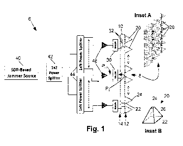
[0009] FIGURE 1 diagrammatically illustrates a radio frequency (RF) jamming
device.
Inset A of FIGURE 1 shows a perspective view of the illustrative differential
segmented
aperture (DSA) of the RF jamming device. Inset B of FIGURE 1 shows a variant
embodiment of the electrically conductive tapered projections.
[0010] FIGURE 2 diagrammatically shows a side sectional view of an
embodiment of
the electrically conductive tapered projections, along with a diagrammatic
representation
of the connection of the balanced port of a chip balun between two adjacent
electrically
conductive tapered projections forming an aperture pixel.
[0011] FIGURE 3 diagrammatically illustrates a jamming station employing
the DSA
of FIGURE 1 on a rotatable turret.
[0012] FIGURE 4 diagrammatically shows arranging a plurality of DSAs of the
type
shown in FIGURE 1 to provide full 360 degrees azimuth jamming.
[0013] FIGURE 5 diagrammatically shows a portable jamming device having a
rifle
form factor, which employs a DSA of the type shown in FIGURE 1.
DETAILED DESCRIPTION
[0014] With reference to FIGURE 1, a diagrammatic view of a jamming device
6 is
shown, which employs a differential segmented aperture (DSA) 8 which is shown
in
diagrammatic side sectional view in the main drawing of FIGURE 1 and in
diagrammatic
perspective view in Inset A of FIGURE 1. The illustrative DSA 8 includes a
printed circuit
board (PCB) 10 having a front side 12 and a back side 14, and an array of
electrically
conductive tapered projections 20 having bases 22 disposed on the front side
12 of the
PCB 10 and extending away from the front side 12 of the PCB 10 and tapering to
terminate in an apex 24. The electrically conductive tapered projections 20
can have any
type of cross-section (e.g. square so as to form faceted electrically
conductive tapered
projections 20' as four-sided pyramids having four facets, as in Inset B,
circular,
hexagonal, i.e. faceted with six facets, octagonal, i.e. faceted with eight
facets, or so
forth). The apex 24' can be flat, as in the nonlimiting illustrative example
four-sided
pyramid electrically conductive tapered projection 20' of Inset B, or can come
to a sharp
point 20 as in the nonlimiting illustrative conical electrically conductive
tapered projections
20, or can be rounded or have some other apex geometry. The rate of tapering
as a
3
CA 03141306 2021-11-18
WO 2020/256886 PCT/US2020/034119
function of height (i.e. distance "above" the base 22, with the apex 24 being
at the
maximum "height") can be constant, or the rate of tapering can be variable
with height,
e.g. the rate of tapering can increase with increasing height so as to form a
projection
with a rounded peak, or can be decreasing with increasing height so as to form
a
projection with a more pointed tip. Similarly, as best seen in FIGURE 1, Inset
A, the
illustrative array of the electrically conductive tapered projections 20 is a
rectilinear array
with regular rows and orthogonal regular columns; however, the array may have
other
symmetry, e.g. a hexagonal symmetry, octagonal symmetry, or so forth. The
sidewalls of
the electrically conductive tapered projections 20 can have various sidewall
shapes, e.g.
a square base and square apex lead to having four flat slanted sidewalls; as
another
example, if the base and apex are circular (or the base is circular and the
apex comes to
a point) then the sidewall is suitably a slanted or tapering cylinder; as yet
another
example, for a hexagonal base and a hexagonal or pointed apex six slanted
sidewalls are
suitable, and so forth.
[0015] With continuing reference to FIGURE 1, the RF aperture further
comprises RF
circuitry, which in the illustrative embodiment includes chip baluns 30
mounted on the
back side 14 of the PCB 10. Each chip balun 30 has a balanced port PB
electrically
connected with two neighboring electrically conductive tapered projections 20
of the array
of electrically conductive tapered projections via electrical feedthroughs 32
passing
through the PCB 10. Each chip balun 30 further has an unbalanced port Pu
connecting
with the remainder of the RF circuitry. As will be further described, each
chip balun 30
thus drives an aperture pixel comprising a pair of projections 20 connected
with its
balanced port PB by power received at its unbalanced port Pu. The illustrative
RF circuitry
further includes a software-defined radio (SDR) based jammer source 40 that
generates
a jamming signal at pre-defined or user-defined frequencies or frequency bands
which
are to be jammed; one or more RF power splitter 42, 44 for splitting the power
generated
by the SDR based jammer source 40 to the unbalanced ports Pu of the chip
baluns 30,
and a power amplifier 46 driving the unbalanced port Pu of each chip balun 30.
In FIGURE
1, the illustrative electrical configuration of the RF circuitry employs first
level 1x2 RF
power splitters 42 and second level 1xN RF power splitters 44 that further
split the power
to the baluns 30. It is alternatively contemplated to employ a single power
splitter or to
4
CA 03141306 2021-11-18
WO 2020/256886 PCT/US2020/034119
employ two (as illustrated), three, or more levels of power splitters,
depending upon the
number of aperture pixels to be driven and the rated power specifications for
the power
splitter components.
[0016] In the illustrative embodiment of FIGURE 1, a compact design is
achieved in
part by employing one or more printed circuit boards (PCBs) including at least
the
illustrative PCB 10 on which are mounted the chip baluns 30. Additional
electronic
components of the RF circuitry (e.g., the power splitters 42, 44, the power
amplifiers 46,
and optionally also components of the SDR based jammer source 40, are suitably
also
mounted on the back side 14 of the PCB 10, and/or on one or more additional
circuit
boards (not shown), which may be mounted in parallel with and spaced apart
from the
illustrated PCB 10 using suitable standoffs; or may be mounted elsewhere, with
the
components of the optional additional PCB(s) (not shown) being electrically
connected
with the unbalanced ports Pu of the chip baluns 30 by electrical wiring. The
illustrative RF
aperture includes chip baluns 30 mounted on the back side 14 of the PCB 10.
Alternatively, the baluns 30 may be otherwise implemented, e.g., as baluns
inscribed into
the PCB 10. In another approach, RF circuitry driving the RF aperture may be
entirely
differential signal chains, in which case the baluns can be omitted.
[0017] The jamming device 6 employs the DSA 8 as the jamming signal output
aperture. The balanced ports PB of the chip baluns 30 connect adjacent (i.e.
neighboring)
pairs of electrically conductive tapered projections 20 of the array to apply
a differential
RF signal received at the unbalanced port Pu of the chip balun 30 between the
two
adjacent electrically conductive tapered projections 20. Operation of pairs of
electrically
conductive tapered projections in radiating RF power is described in
Steinbrecher, U.S.
Pat. No. 7,420,522 which is incorporated herein by reference in its entirety.
The tapering
of the electrically conductive tapered projections 20 presents a separation
between the
two electrically conductive tapered projections 20 that continuously varies
with the
"height", i.e. with distance "above" the base 22 of the electrically
conductive tapered
projections 20. This provides the DSA 8 with broadband RF functionality since
a large
range of RF wavelengths can be coupled corresponding to the range of
separations
between the adjacent electrically conductive tapered projections 20 introduced
by the
tapering. The DSA 8 thus has differential RF transmit elements corresponding
to the
CA 03141306 2021-11-18
WO 2020/256886 PCT/US2020/034119
adjacent pairs of electrically conductive tapered projections 20. These
differential RF
transmit elements are referred to herein as aperture pixels. For example, the
illustrative
rectilinear 6x6 array of adjacent electrically conductive tapered projections
20 shown in
Inset A of FIGURE 1 has five aperture pixels along each row (or column) of six
electrically
conductive tapered projections 20. More generally, for a rectilinear array of
projections
having a row (or column) of N electrically conductive tapered projections 20,
there will be
a corresponding N-1 aperture pixels along the row (or column).
[0018] The SDR based jammer source 40 advantageously employs a suitably
programmed microprocessor or microcontroller and associated digital
electronics (e.g.
random access memory or other electronic storage) to generate a digital
jamming signal
at a desired set of one or more frequencies to be jammed that is converted to
an analog
jamming signal using digital-to-analog (D/A) circuitry. Use of a SDR
advantageously
promotes configurability as the choice of jamming frequencies (or frequency
bands) can
be configured in software of the SDR. However, it is alternatively
contemplated to employ
an analog jammer source in place of the SDR based jammer source 40.
[0019] In operation, the jammer source 40 is configured to output a jamming
signal at
one or more frequencies or frequency bands which are to be jammed. The RF
electronics
42, 44, 46 are configured to amplify and feed the jamming signal to the DSA 8,
whereby
the DSA 8 emits a jamming beam at the one or more frequencies or frequency
bands
which are to be jammed. The configuration of the jammer source may be hard
wired, e.g.
the jammer source may be an analog RF circuit that generates an RF signal at
the one
or more frequencies or frequency bands which are to be jammed. In the
illustrative
embodiment, the SDR based jammer source 40 is configured by software
programming
of the SDR to generate a digital signal at the one or more frequencies or
frequency bands
which are to be jammed that is then converted to an analog RF signal by a D/A
converter.
In a variant embodiment, the SDR may generate the digital signal mapped to the
one or
more frequencies or frequency bands which are to be jammed, which is then
converted
to an analog RF signal by a D/A converter and then heterodyned in the analog
domain to
the one or more frequencies or frequency bands which are to be jammed. These
are
merely some non-limiting illustrative examples, and more generally any SDR
based RF
signal generation system can be employed as the SDR based jammer source 40. In
some
6
CA 03141306 2021-11-18
WO 2020/256886 PCT/US2020/034119
embodiments, the SDR includes a user interface (e.g., see the examples
described with
reference to FIGURES 3 and 5) via which a user can select the one or more
frequencies
or frequency bands which are to be jammed.
[0020] The described configuration employing the PCB 10 with its front side
12 serving
as a mounting surface for the electrically conductive tapered projections 20
of the DSA 8
and the chip baluns 30 mounted on its back side 14 advantageously enables the
jamming
device 6 to be made compact and lightweight. As described next, embodiments of
the
electrically conductive tapered projections 20 further facilitate providing a
compact and
lightweight jamming device 6.
[0021] FIGURE 2 shows a side sectional view of one illustrative embodiment
in which
each electrically conductive tapered projection 20 is fabricated as a
dielectric tapered
projection 50 with an electrically conductive layer 52 disposed on a surface
of the
dielectric tapered projection 50. The dielectric tapered projections may, for
example, be
made of an electrically insulating plastic or ceramic material, such as
acrylonitrile
butadiene styrene (ABS), polycarbonate, or so forth, and may be manufactured
by
injection molding, three-dimensional (3D) printing, or other suitable
techniques. The
electrically conductive layer 52 may be any suitable electrically conductive
material such
as copper, a copper alloy, silver, a silver alloy, gold, a gold alloy,
aluminum, an aluminum
alloy, or so forth, or may include a layered stack of different electrically
conductive
materials, and may be coated onto the dielectric tapered projection 50 by
vacuum
evaporation, RF sputtering, or any other vacuum deposition technique. FIGURE 2
shows
an example in which solder points 54 are used to electrically connect the
electrically
conductive layer 52 of each dielectric tapered projection 20 with its
corresponding
electrical feedthrough 32 passing through the PCB 10. FIGURE 2 also shows the
illustrative connection of the balanced port PB of one chip balun 30 between
two adjacent
electrically conductive tapered projections 20 via solder points 56.
[0022] It is to be understood that the DSA manufacturing design of FIGURE 2
is merely
an illustrative example, and numerous other approaches for fabricating the DSA
8 are
contemplated. For example, the electrically conductive tapered projections 20
may be
solid metal cones (or otherwise shaped tapered projections), formed as
freestanding
metal shells by sheet metal punching or other sheet metal processing
techniques, or so
7
CA 03141306 2021-11-18
WO 2020/256886 PCT/US2020/034119
forth. Moreover, the illustrative PCB 10 can be replaced by another DSA
substrate, with
electrical wiring provided to electrically connect the aperture pixels of the
DSA to the RF
electronics. These are merely further illustrative examples.
[0023] In the illustrative design of FIGURE 1, each power amplifier 46
drives an
individual aperture pixel of the DSA 8. Said another way, each pixel power
amplifier 46 is
connected to amplify the jamming signal fed to a single corresponding aperture
pixel of
the DSA 8. Accordingly, the power amplifiers 46 are also referred to herein as
pixel power
amplifiers 46. The gain provided by the pixel power amplifier 46 (in
combination with any
optional further amplifiers, not shown, optionally interposed between the SDR
based
jammer source 40 and the pixel power amplifier 46) is referred to herein as
the aperture
gain. As the jamming signal input to each aperture pixel is individually
amplified by its
corresponding pixel power amplifier 46, the individual pixel power amplifiers
46 can be of
lower power rating as compared with an RF aperture that is driven by a jamming
signal
amplified by a single power amplifier driving the entire RF aperture.
[0024] Moreover, the power at any point in space in the far field is an
additive
combination of the power from each aperture pixel. This is referred to as the
spatial gain.
[0025] These two gains: aperture gain due to the size of the effective
aperture, and
spatial gain due to the combination of power from the individual aperture
pixels in the far
field, are additive. Consequently, the Effective Isotropic Radiated Power
(EIRP) in the far
field is the additive sum of the aperture gain and spatial gain in decibels.
This enables the
jamming device 6 to output high jamming power in the far field while using
relatively small
pixel power amplifiers 46. For example, if a 16 pixel DSA, each having a 30
dBm power
amplifier connected as shown in FIGURE 1, configured as a 5"x5" physical
aperture (that
is, five inch square physical aperture) operating with 100% efficiency (that
is, the physical
aperture equals the effective aperture), then the total EIRP in the far field
will be the sum
of the two gains. So, for a jamming frequency of 2.4 GHz, the calculated
aperture gain
will be approximately 7 dBi and the spatial gain will be equal to 10*Log(16)
or 12 dB.
Since each pixel has a 30 dBm amplifier connected, the total EIRP would be 30
dBm +
12 dB + 7 dB or 49 dBm. If each of the power amplifiers has a 30 dB gain, and
the splitting
loss is 12 dB (16 power divisions), an SDR would only have to source 30 dBm ¨
30 dB +
12 dB or 12 dBm to realize the full 49 dBm EIRP, neglecting small insertion
losses.
8
CA 03141306 2021-11-18
WO 2020/256886 PCT/US2020/034119
[0026] Furthermore, this high EIRP can be provided over a wide beam angle.
A square
planar DSA results in a beam pattern that is directional in nature. An
estimate of the beam
width (in radians) of a square, flat DSA is given by the following equation:
( 1 A2 \
Beamwidth(rad) = 2 = cos-1 (1)
2n-Aeff )
where A is the wavelength of the RF signal, and Aeff is the effective area of
the RF
aperture. As the effective area (Aeff) decreases, the beamwidth increases
(albeit with a
lower gain as the total power is spread out into the larger beamwidth).
[0027] Still further, with reference back to FIGURE 2, the DSA 8 is a
broadband RF
aperture due to the large range of frequencies that can couple with the
aperture pixels.
FIGURE 2 diagrammatically indicates that, at a "height" H above the base 22 of
the
electrically conductive tapered projections 20, the projections 20 of the
aperture pixel are
spaced apart by a distance D(H). This spacing range from a minimum spacing at
the base
22 of D(0) to a maximum spacing at the apex 24 of D(Hapex). The band of
wavelengths
that can couple then corresponds to the continuous range of spacings
[D(0),D(Hapex)],
and can be recast as the aperture frequency band using the conversion fA = c
where f
is frequency, A is the wavelength, and c is the speed of light.
[0028] The combination of the SDR based jammer source 40 (see FIGURE 1) and
the
wide bandwidth of the DSA 8, along with the efficiently obtained high far
field power
achievable with the DSA 8, enables the jamming device 6 to be programmed in
the field
(or, alternatively, pre-programmed) to jam radio signals at any desired
frequency,
combination of frequencies, band of frequencies, or set of disjoint bands of
frequencies.
[0029] With non-limiting illustrative reference to FIGURES 3-5, the jamming
device 6
of FIGURE 1 can be deployed in various ways. FIGURE 3 illustrates a deployment
on a
rotatable turret 60 that enables a single planar DSA 8 to be rotated about a
vertical axis
62 so as to be positioned at a desired azimuth angle. The turret 60 may be a
fixed
mounting, or could be mounted in the bed of a truck or other vehicle (not
shown) in order
to provide a mobile jamming station. The illustrative turret 60 positions the
DSA 8 to
generate a horizontally directed jamming beam. Alternatively, the DSA 8 could
be
9
CA 03141306 2021-11-18
WO 2020/256886 PCT/US2020/034119
mounted at some other angle, e.g. at a shallow elevation to increase jamming
capacity at
higher elevations. In another contemplated variant, a further joint (not
shown) could be
provided to enable tilting of the DSA 8 about a horizontal axis to enable
jamming directed
at a user-selected elevation. The geometry of the DSA 8 could also be tuned to
provide
an asymmetric beam. For example, a wider vertical beamwidth compared with a
narrower
horizontal beamwidth could be achieved by making the DSA rectangular with a
longer
horizontal dimension and a shorter vertical dimension. In one suitable
implementational
approach, the power splitters 42, 44 and pixel power amplifiers 46 shown in
FIGURE 1
are integrated with the planar DSA 8 (e.g. being mounted on the PCB 10 and, if
needed,
on an additional one or more PCBs mounted in parallel with the illustrated PCB
10 using
suitable standoffs. The SDR based jammer source 40 may be mounted remotely
from the
DSA 8, for example in the bed or cab of the vehicle in embodiments in which
the rotating
turret 60 is vehicle-mounted. In this approach, for example, the SDR based
jammer
source 40 may comprise a notebook computer providing the microprocessor and
non-transitory storage medium (e.g. hard drive or solid state drive, SSD)
storing the SDR
software, with the computer connected via a USB port or other digital
communication link
with external intermediary RF circuitry including a D/A converter and an
optional power
(pre-)amplifier feeding into the base-level power splitter(s) 42 of FIGURE 1.
Advantageously, the computer could also run software providing control for the
rotation
mechanism of the turret 60, so that a user sitting in the cab of the vehicle
could set the
azimuth direction of the DSA 8 via the turret 60 (and the elevation, if a
further elevation
adjustment is provided for the DSA 8) and select the frequency or frequencies
or
frequency band or bands to be jammed, as well as the total jamming power.
[0030] FIGURE 4 illustrates an example in which four DSAs 8 are arranged at
0 degree, 90 degree, 180 degree, and 270 degree azimuth angles (referenced to
an
arbitrary 0 degree azimuth angle) forming a cube so as to provide full 360
degree azimuth
coverage. This assumes that each DSA 8 has a horizontal beamwidth of at least
90
degrees. If the DSAs have a smaller horizontal beamwidth than this, then
additional
planar DSAs may be added, e.g. six planar DSAs at 0, 60, 120, 180, 240, and
300 degree
azimuth angles thereby forming a hexagon. In a variant embodiment, the
illustrative flat
DSAs 8 can be replaced by DSAs having a curved surface to increase the
beamwidth
CA 03141306 2021-11-18
WO 2020/256886 PCT/US2020/034119
(albeit possibly at the loss of some spatial gain). For example, the curved
surface could
be manufactured to be conformal with a curved surface of the fuselage of an
aircraft or
unmanned aerial vehicle (UAV), or to be conformal with the hull of an ocean-
going ship
or submarine, or to be conformal with a surface of a round or cylindrical
orbiting satellite,
or so forth. Each planar DSA 8 in the embodiment of FIGURE 4 includes the PCB
10 and
the RF electronics as shown in FIGURE 1, except that in the embodiment of
FIGURE 4 it
is contemplated for a single instance of the SDR based jammer source 40 to
drive all four
DSAs 8 of the embodiment of FIGURE 4 by way of a further 1x4 power splitter
(not
shown). In one contemplated practical implementation, the assembly shown in
FIGURE
4 is mounted on a fixed tower to provide omnidirectional jamming over the full
360
degrees of azimuth.
[0031] FIGURE 5 illustrates an example of a portable jamming device having
a rifle
form factor, which employs a single instance of the planar DSA 8. The rifle
form factor is
provided by a rifle-shaped housing 70 having a barrel 72, and the DSA 8 is
mounted on
the distal end of the barrel 72 with the array of electrically conductive
tapered projections
20 facing outward from the end of the barrel 72. (Said another way, the array
of electrically
conductive tapered projections 20 are oriented to generate the jamming beam
directed
outward from the barrel in the direction that a bullet would be fired if the
rifle-shaped
housing 70 were an actual rifle). In the illustrative embodiment, the SDR
based jammer
source 40 (indicated diagrammatically by dashed lines in FIGURE 5 to indicate
an internal
component). The power splitters 42, 44 and pixel power amplifiers 46 may be
mounted
integrally with the DSA 8 as described for the embodiment of FIGURE 3, or may
be
disposed inside the rifle-shaped housing 70 and connected with the DSA 8 by
suitable
wiring in the "barrel" of the rifle-shaped housing 70. Some portable jamming
devices
having rifle form factors are described in Stamm et al., U.S. Pat. No.
10,020,909 issued
July 10, 2018 and Morrow et al., U.S. Pat. No. 10,103,835 issued October 16,
2018, both
of which are incorporated herein by reference in their entireties. The rifle-
shaped housing
70 further supports a trigger 74 by which an operator energizes the DSA 8 to
emit a
jamming beam. The illustrative rifle-shaped housing 70 further has a display
76 and user
controls 78 mounted thereon by which a user can read and adjust settings of
the SDR
based jamming source 40, respectively. (While user controls 78 separate from
the display
11
CA 03141306 2021-11-18
WO 2020/256886 PCT/US2020/034119
76 are shown, it is contemplated for the display and the user controls to be
integrated
together, e.g. in the form of a touch-screen display in which user controls
are displayed
on the display and are operated by user touches to the display). This enables
the user to
select the jamming frequency, frequencies, frequency band, or frequency bands
in the
field. (Other user interfacing hardware is contemplated, for example a mobile
device
application program or "app" running on a cellphone, tablet computer, or the
like may be
used to interface wirelessly with the SDR based jamming source 40). The
portable
jamming device of FIGURE 5 can be useful, for example, in disrupting operation
of an
unmanned aerial vehicles (UAV), sometimes referred to as a drone, if it is
impinging upon
the controlled airspace of a commercial airport or other security-sensitive
location.
[0032] In some embodiments, it is contemplated for the jamming device 6 to
provide
jamming capability over a broad spectrum of communications from 4 MHz to 6
GHz,
although a larger, smaller, or different broad spectrum operation range is
also
contemplated. In one non-limiting illustrative example, the jamming device 6
provides
jamming capability over a broad spectrum encompassing the unlicensed
"Industrial
Scientific Manufacturing" (ISM) bands in which many drones are currently
operated.
Again, these are merely non-limiting illustrative examples, and the broad
spectrum of
operation is suitably designed based on the shapes of the electrically
conductive tapered
projections 20 so as to design the D(H) function described with reference to
FIGURE 2
and by the operating frequency ranges of the SDR based jammer source 40 and
power
distribution/amplification RF electronics 30, 42, 44, 46.
[0033] The jamming device 6 operates in transmit mode to output a jamming
beam. In
some embodiments (including the illustrative embodiment), the jamming device 6
is not
configured to receive an RF signal via the DSA 8. For example, the jamming
device 6
does not include RF electronics configured to receive an RF signal via the DSA
8.
Similarly, the SDR of the SDR based jammer source 40 is not programmed to
process a
received RF signal.
[0034] In other embodiments, it is contemplated to provide receive
capability to assist
in the jamming process. For example, it is contemplated (although not
illustrated) to
include receive capability (e.g. the illustrated RF electronics can be
configured to receive
an RF signal via the DSA 8, for example using suitable RF switches to switch
out the
12
CA 03141306 2021-11-18
WO 2020/256886 PCT/US2020/034119
transmit power amplifiers 46 and switch in receive amplifiers (not shown),
with the splitters
42, 44 being RF combiner/splitter components to enable conveying the received
RF
signal, and the SDR based jamming source 30 being further programmed to
process the
received RF signal. For example, such RF receive capability may be useful in
the
embodiment of FIGURE 5 to automatically set the one or more frequencies or
frequency
bands which are to be jammed. This can be done by receiving the broadband
signal at
intervals while the trigger 74 is pulled (indicating the device is pointed at
the UAV to be
jammed). Under the assumption that the strongest RF signal in this state will
be at the
one or more frequencies or frequency bands transmitted by the UAV, the SDR
based
jammer source 40 can then automatically configure (by suitable programming of
the SDR)
to output a jamming signal at the one or more frequencies or frequency bands
which
dominate the received RF signal, so as to jam those frequencies.
The preferred embodiments have been illustrated and described.
Obviously,
modifications and alterations will occur to others upon reading and
understanding the
preceding detailed description. It is intended that the invention be construed
as including
all such modifications and alterations insofar as they come within the scope
of the
appended claims or the equivalents thereof.
13