Note: Descriptions are shown in the official language in which they were submitted.
CA 03143516 2021-12-14
WO 2021/102019
PCT/US2020/061085
SHIELDING OF ELECTRONICS FROM MAGNETIC FIELDS
RELATED APPLICATIONS
This application claims the benefit under 35 U.S.C. 119(e) of the filing
date of U.S.
Provisional Application Serial No. 62/939,151, filed November 22, 2019, the
entire contents of
which is incorporated herein by reference.
BACKGROUND
1. Technical Field
The techniques described herein relate generally to shielding of electronics
from
magnetic fields such as those produced by windings (e.g., in a wireless power
transfer system).
2. Discussion of the Related Art
Various devices include coils that produce magnetic fields. Examples include
inductors,
transformers and coils of a wireless power transfer system, by way of example.
A wireless power transfer system can transfer energy wirelessly through
magnetic
coupling. Various types of wireless power transfer systems exist, such as
inductive systems and
resonant systems.
SUMMARY
Some aspects relate to an apparatus, comprising: a coil; an electronic
circuit; and an
electrically conductive shield positioned between the coil and the electronic
circuit.
The apparatus may further comprise a magnetic core magnetically coupled to the
coil,
wherein the electrically conductive shield is positioned between the magnetic
core and the
electronic circuit.
The electrically conductive shield may have a planar section.
The electrically conductive shield may have an overhang protruding on a side
of the
electrically conductive shield facing the electronic circuit.
The overhang may have at least a portion that is straight.
The overhang may have at least a portion that is curved.
The overhang may be curled in a curved manner or a stepped manner in an inward
direction or an outward direction.
The magnetic core may have an overhang protruding on a side of the magnetic
core
facing the electronic circuit.
1
CA 03143516 2021-12-14
WO 2021/102019
PCT/US2020/061085
The electrically conductive shield may comprise a metal.
The electrically conductive shield may have a thickness of greater than a skin
depth at a
fundamental frequency of current in the coil.
The electronic circuit may be electrically coupled to the coil.
The coil may be configured to produce a magnetic field and the electronic
circuit may be
within the magnetic field.
The coil may be proximate the electronic circuit.
The electronic circuit may comprise an inverter of a wireless power
transmitter or a
rectifier of a wireless power receiver.
Some aspects relate to an apparatus, comprising: a coil; an electronic
circuit; and a
magnetic core magnetically coupled to the coil, the magnetic core having an
overhang protruding
on a side of the magnetic core facing the electronic circuit.
The apparatus may further comprise an electrically conductive shield between
the
magnetic core and the electronic circuit.
The electrically conductive shield may have an overhang protruding on a side
of the
electrically conductive shield facing the electronic circuit.
The overhang of the magnetic core may have a first overhang section protruding
on the
side of the magnetic core facing the electronic circuit and the magnetic core
may also have a
second overhang section protruding in an inward direction.
The electrically conductive shield may have a planar section.
The electrically conductive shield may comprise a metal.
The electrically conductive shield may have a thickness of greater than a skin
depth at a
fundamental frequency of current in the coil.
The overhang of the electrically conductive shield may have at least a portion
that is
straight.
The overhang of the electrically conductive shield may have at least a portion
that is
curved.
The overhang of the electrically conductive shield may be curled in a curved
manner or a
stepped manner in an inward direction or an outward direction.
The electronic circuit may be electrically coupled to the coil.
The coil may be configured to produce a magnetic field and the electronic
circuit may be
within the magnetic field.
The coil may be proximate the electronic circuit.
2
CA 03143516 2021-12-14
WO 2021/102019
PCT/US2020/061085
The electronic circuit may comprise an inverter of a wireless power
transmitter or a
rectifier of a wireless power receiver.
The apparatus may include an inductor or transformer comprising the coil.
The apparatus may be used in wireless power transfer.
Some aspects relate to a method of using the apparatus.
The foregoing summary is provided by way of illustration and is not intended
to be
limiting.
BRIEF DESCRIPTION OF DRAWINGS
In the drawings, each identical or nearly identical component that is
illustrated in various
figures is represented by a like reference character. For purposes of clarity,
not every component
may be labeled in every drawing. The drawings are not necessarily drawn to
scale, with
emphasis instead being placed on illustrating various aspects of the
techniques and devices
described herein.
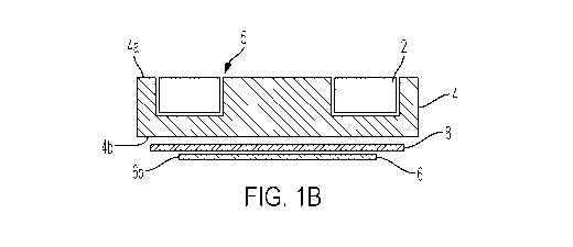
FIG. lA shows a cross-section of a winding within a magnetic core.
FIG. 1B shows that a conductive shield may be positioned between the
electronic circuit
and the magnetic core, according to some embodiments.
FIG. 2 shows the bottom plan view of a winding with a conductive shield
positioned
between the electronic circuit and the magnetic core, according to some
embodiments.
FIGS. 3A-3E show a conductive shield having an overhang which may have various
shapes, according to some embodiments.
FIGS. 4A-4B show a magnetic core having an overhang, which may have various
shapes,
as well as a conductive shield, according to some embodiments.
FIGS. 5A-5B show a magnetic core having an overhang and no conductive shield,
according to some embodiments.
FIGS. 6A-6B show a magnetic core having an overhang portion that is physically
separated from the rest of the magnetic core, according to some embodiments.
FIGS. 7A-7D show examples of structures including both a magnetic core with an
overhang and a conductive shield with an overhang, according to some
embodiments.
DETAILED DESCRIPTION
A wireless power transfer system includes a wireless power transmitter and a
wireless
power receiver, each of which includes a power transfer coil (also herein
termed "coil" or
"winding"). A wireless power transmitter may include a transmit coil that may
be coupled to a
3
CA 03143516 2021-12-14
WO 2021/102019
PCT/US2020/061085
power source via power electronics. The power electronics may invert a DC
(direct current)
signal into an AC (alternating current) signal that can be transmitted
wirelessly to a wireless
power receiver through electromagnetic induction. A wireless power receiver
may include a
receive coil and power electronics (e.g., a rectifier) that couples the
receive coil to a load. In
operation, a wireless power transmitter and receiver are physically separated
from one another by
some distance, and the wireless power transmitter inductively transfers power
to the wireless
power receiver.
In many applications, proximity of electronics and the transmit or receive
coils may be
necessary or convenient. For example, placement of electronic circuits such as
power electronic
circuits on the back of an transmit coil or a receive coil can reduce the
overall footprint of a
wireless power transmitter or receiver.
The performance of a wireless power transfer system may be constrained by the
magnetic
coupling factor (k) between the coils and the quality factor (Q) of the coils.
The magnetic
coupling factor (k) may be limited by the wireless gap, so achieving high-Q
can often help
achieve high-performance wireless power transfer.
The inventors have recognized and appreciated that the placement of an
electronic circuit
(e.g., power electronics circuit) proximal to the wireless power transmit or
receive coils can be
detrimental to the Q of the coils. Eddy currents induced in the electronic
circuit by the magnetic
field create additional power loss ¨ limiting the Q of the coils. A similar
issue may arise with
other devices (e.g., transformers or inductors) with a current-carrying coil
positioned near
electronics which may or may not be electrically coupled to the coil.
FIG. 1A shows a cross-section of a winding 2 within a magnetic core 4, on the
front side
4a of the magnetic core 4. The magnetic core 4 may include a cavity 5 for
accommodating the
winding 2. The winding 2 need not fill the entire cavity 5, but may fill the
cavity 5. The cavity 5
and winding 4 may have any suitable shape in plan view, such as an annular
shape, or an
elliptical shape, for example. An electronic circuit 6, which may include a
printed circuit board
(PCB) with conductive traces 15 and other components 16 (e.g., an inverter, a
rectifier circuit,
etc.), as illustrated in FIG. 2, is placed on the back 4b of the magnetic core
4. The winding 2
may be a transmit coil of a wireless power transmitter. When the winding 2 is
a transmit coil,
the electronic circuit 6 may include transmit power electronics such as an
inverter, for example,
which is electrically connected to the transmit coil to drive the transmit
coil. Alternatively, the
winding 2 may be a receive coil of a wireless power receiver. When the winding
2 is a receive
coil, the electronic circuit 6 may include receive power electronics such as a
rectifier, for
example, which is electrically connected to the receive coil to receive and
process power from
4
CA 03143516 2021-12-14
WO 2021/102019
PCT/US2020/061085
the receive coil. Current within the winding 2 produces a magnetic field that,
in turn, produces
eddy currents in the components on the PCB and in the traces of the PCB. Power
loss (also
termed "loss" or "losses") is concentrated near the edges of conductors so the
edge of each trace
incurs an especially large amount of loss.
The inventors have recognized and appreciated that an electronic circuit 6 may
be
shielded from the magnetic field by providing an electrically conductive
shield (also termed a
"conductive shield" or "shield") between the winding 2 and the electronic
circuit 6. FIG. 1B
shows that a conductive shield 8 may be positioned between the electronic
circuit 6 and the
magnetic core 4. Such a conductive shield 8 may be realized in a variety of
ways. For example,
a conductive material may be placed on the back 4b of the magnetic core 4 or
on the bottom 6b
of a printed circuit board (PCB), or the PCB may be constructed so that the
bottom layer (layer
closest to the magnetic core 4) is a region of conductive material.
FIG. 2 shows a bottom plan view corresponding to FIG. 1B, in which a
conductive shield
8 is positioned between the electronic circuit 6 and the magnetic core 4. In
this example, the
magnetic core 4, electronic circuit 6 and conductive shield 8 each has a
circular shape. However,
the techniques and structures described herein are not limited in this
respect, as the magnetic core
4, electronic circuit 6 and conductive shield 8 may have any suitable shapes,
and their shapes
may be the same as one another or different from one another. In this example,
the magnetic
core 4 takes up more area in plan view than the conductive shield 8 and
completely covers
conductive shield 8, which in turn takes up more area in plan view than the
electronic circuit 6
and completely covers electronic circuit 6. However, the techniques described
herein are not
limited in these respects, as they may have different relative areas or may
not completely cover
one another. It should be appreciated that in some embodiments conductive
shield 8 completely
covers electronic circuit 6 to provide a high degree of shielding.
The conductive shield 8 may be made of any electrically conductive material or
combination of materials, including but not limited to one or more metals such
as silver, copper,
aluminum, gold and titanium, and non-metallic materials such as graphite. The
electrically
conductive material or combination of materials may have an electrical
conductivity of higher
than 1 MS/m, optionally higher than 200 kS/m. A complete shielding of the
electronic circuit 6
from the magnetic field may require a conductive shield that is thicker than a
skin depth at the
operating frequency. The operating frequency is the fundamental frequency of
current in the
coil, which may be any suitable frequency. Some examples of wireless power
transfer that may
be performed by the devices described herein include inductive and resonant
wireless power
transfer. However, the techniques described herein are not limited in this
respect. Further,
5
CA 03143516 2021-12-14
WO 2021/102019
PCT/US2020/061085
complete shielding is not required, and a conductive shield thinner than, but
close to (e.g., greater
than 10% or 50% of a skin depth) a skin depth may also be effective in
reducing the loss in the
components on the PCB and in the traces of the PCB. However, the techniques
and devices
described herein are not limited as to the particular material of the
conductive shield.
The magnetic core 4 may be, wholly or partially, made of one or more
ferromagnetic
materials which has/have a relative permeability of greater than 1, optionally
greater than 10, and
in some cases no more than 1 million. The magnetic core materials may include,
but are not
limited to, one or more of iron, various steel alloys, cobalt, ferrites
including manganese-zinc
(MnZn) and/or nickel-zinc (NiZn) ferrites, nano-granular materials such as Co-
Zr-O, and
powdered core materials made of powders of ferromagnetic materials mixed with
organic or
inorganic binders. However, the techniques and devices described herein are
not limited as to
the particular material of the magnetic core 4. The shape of the magnetic core
may be: a pot
core, a sheet (I core), a sheet with a center post, a sheet with an outer rim,
RM core, P core, PH
core, PM core, PQ core, E core, EP core, or EQ core, by way of example.
However, the
techniques and devices described herein are not limited to a particular
magnetic core shape.
The winding 2 may be, wholly or partially, made of conductive materials
including but
not limited to one or more metals such as silver, copper, aluminum, gold. The
winding 2 may be
constructed, but not limited to, using wire, magnet wire, stranded wire, litz
wire, printed circuit
board traces, conductors laminated on a substrate, foil layers, multilayer
self-resonant structures,
modified multilayer self-resonant structures, solid metal, or any combination
thereof.
The inventors have recognized and appreciated that the shape of the shield 8
can impact
the magnitude of the power losses caused by eddy currents. In some
embodiments, the shield 8
has an edge that is shaped to guide the magnetic field around the edge of the
conductive shield 8.
For example, the edge of the shield 8 may have an "overhang" extending in the
direction of the
electronics protected by the conductive shield. The overhang may have various
shapes,
examples of which are described below.
Alternatively or additionally, the magnetic core may have a region that is
shaped to guide
the magnetic field around the edge of the conductive shield, and may extend in
the direction of
the electronics being protected. Such a region of a magnetic core is also
referred to as an
"overhang." One or more "overhangs" of electrically conductive material,
magnetic material, or
both can be used to reduce power loss induced in the electronic circuit by
eddy currents. This
allows a circuit or other lossy material to be placed physically close to the
winding 2 without
limiting the Q of the winding 2. Various embodiments are described below.
6
CA 03143516 2021-12-14
WO 2021/102019
PCT/US2020/061085
In some embodiments, the conductive shield 8 has one or more overhangs 12 that
extend
away from the magnetic core any or all sides of the shield 8. Examples of
overhang shapes are
shown in FIGS. 3A-3D. The overhang of conductive material reduces lateral
current crowding
in the conductive shield by shaping the edge of the shield to more closely
follow the magnetic
flux lines. This can reduce losses in the shield up to 40% or more. This can
be implemented
using various techniques.
FIG. 3A shows an embodiment of a conductive shield with an overhang that can
be
manufactured using standard PCB technology. The position of the overhang 12 in
plan view is
shown in FIG. 2. In the embodiment of FIG. 3A, the shield 8 includes a planar
portion 11 and an
overhang 12a that extends from the planar portion 11 at a 90 degree angle to
the planar portion
11 in the direction away from the magnetic core 4. The bottom conductive layer
of a PCB can
form the planar portion 11 of the shield 8 and vias in the PCB can be used to
form the overhang
12a. The vias may be formed around the perimeter of the planar portion 11. As
another
example, edge plating on a PCB may be used to form the overhang 12a.
As another example, FIG. 3B depicts a round overhang 12b. Round overhang 12b
can be
created by attaching (e.g., soldering) a wire to the bottom edge of a planar
portion 11 of the
shield, for example. The round overhang 12b may extend around the perimeter of
the planar
portion 11.
FIG. 3C shows an example of a shield 8 with a curved overhang 12c at the edge
of the
planar portion 11, curving toward the electronic circuit 6 and away from the
magnetic core 4.
FIG. 3D shows an example of a shield with an L-shaped overhang 12d that has a
section
12d1 extending downward, away from the magnetic core 4, and a section 12d2
extending toward
the electronic circuit 6. Section 12d1 may extend from the planar portion 11
at a 90 degree angle
to the planar portion 11. Section 12d2 may extend from the section 12d1 at a
90 degree angle to
the section 12d1, in an inward direction. However, the techniques described
herein are not
limited to the number of sections in the overhang 12, or their angles with
respect to one another.
FIG. 3E shows the performance of the same and additional shapes as shown in
FIGS. 3A-
3D. FIG. 3E shows various shapes of conductive shields with overhangs and the
simulated
performance increase (power loss reduction) compared to a similar shield with
no overhangs.
Each illustration depicts the shape of an edge of an overhang 12. As discussed
above, the
overhang may extend in a direction away from the magnetic core 4.
In some embodiments, the magnetic core 4 may have one or more overhangs 14
extending on the side of the electronic circuit 6. One or more overhangs 14 of
magnetic core
7
CA 03143516 2021-12-14
WO 2021/102019
PCT/US2020/061085
material may help to shape the magnetic field around the conductive shield 8
to reduce power
loss. The position of the overhang 14 in plan view is shown in FIG. 2.
FIG. 4A shows an embodiment with a single section of core overhang 14a.
Section 14a
may be an extension of the magnetic core material that extends on the side of
the electronic
circuit 6 and shield 8. The section 14a may extend around the perimeter of the
magnetic core 4,
as shown in FIG. 2. Section 14a may help to shape the magnetic field so that
it extends around
the electronic circuit 6. In some embodiments, the overhang 14 and magnetic
core form a cavity
25 in which the electronic circuit 6 and shield 8 are disposed. In some
embodiments, the
electronic circuit 6 may be completely within the cavity 25 (e.g., above the
lowest portion of the
overhang 14). However, the techniques and structures described herein are not
limited in this
respect, as the electronic circuit 6 may be partially within the cavity 25 in
some embodiments.
FIG. 4B shows an embodiment with two sections of core overhang 14a and 14b.
Section
14b may extend inwardly at an angle of 90 degrees with respect to overhang
14a. Overhang
section 14b may help to further shape the field so that it extends around the
electronic circuit 6.
The overhang section 14b may be at a position below electronic circuit 6 but
not overlapping
electronic circuit 6 in cross section, as shown in FIG. 4B. However, in other
embodiments
overhang section 14b may overlap with electronic circuit 6 in cross section.
Finite element simulations show that the addition of this core material
overhang can
reduce shield loss by 55% for the embodiment of FIG. 4A and 61% for the
embodiment of FIG.
4B.
An overhang 14 of core material can be used even if a conductive shield 8 is
not present,
as it will help straighten the field lines around the conductive traces of the
printed circuit board
and reduce loss. FIG. 5A shows an embodiment similar to the embodiment of FIG.
4A, but
without a shield 8. FIG. 5B shows an embodiment similar to the embodiment of
FIG. 4B, but
without a shield 8.
In some embodiments, a magnetic core overhang can be implemented such that the
overhang is physically separated from the rest of the magnetic core material.
FIGS. 6A and FIG.
6B show such implementations. FIG. 6A shows a magnetic core overhang 14c
similar to
overhang 14a, but physically separated from the rest of the magnetic core 4 by
a gap 15. The
gap 15 may include a non-magnetic material such as air, a non-magnetic
adhesive, or any other
suitable material. FIG. 6B shows a magnetic core overhang similar to that of
FIG. 4B with a
portion 14d extending inwardly from the portion 14c, but with a gap 15
separating the overhang
14c,d from the rest of the magnetic core 4.
8
CA 03143516 2021-12-14
WO 2021/102019
PCT/US2020/061085
In some embodiments, overhangs may be included in both the magnetic core and
the
conductive shield. Any shape of magnetic core overhang may be combined with
any shape of
conductive shield overhang. For example, FIG. 7A shows a single-segment shield
overhang 12a
as illustrated in FIG. 3A and a single-segment magnetic core overhang 14a as
illustrated in FIG.
4A, the combination of which results in 50.4% reduction in shield loss. FIG.
7B shows a double-
segment magnetic core overhang 14a, b as shown in FIG. 4B with a single-
segment shield
overhang 12a as illustrated in FIG. 3A, which results in a 65.7% reduction in
shield loss. FIG.
7C shows a single-segment magnetic core overhang 14a as illustrated in FIG. 4A
and a double-
segment shield overhang 12d, as shown in FIG. 3D, which results in a 65.5%
reduction in shield
loss. FIG. 7D shows a double-segment shield overhang 12d, as shown in FIG. 3D
and a double-
segment magnetic core overhang 14a, b as shown in FIG. 4B, which results in a
70.3% reduction
in shield loss. The combination approach can be utilized with any combination
of overhangs.
Various aspects of the apparatus and techniques described herein may be used
alone, in
combination, or in a variety of arrangements not specifically discussed in the
embodiments
described in the foregoing description and is therefore not limited in its
application to the details
and arrangement of components set forth in the foregoing description or
illustrated in the
drawings. For example, aspects described in one embodiment may be combined in
any manner
with aspects described in other embodiments.
Use of ordinal terms such as "first," "second," "third," etc., in the claims
to modify a
claim element does not by itself connote any priority, precedence, or order of
one claim element
over another or the temporal order in which acts of a method are performed,
but are used merely
as labels to distinguish one claim element having a certain name from another
element having a
same name (but for use of the ordinal term) to distinguish the claim elements.
Also, the phraseology and terminology used herein is for the purpose of
description and
should not be regarded as limiting. The use of "including," "comprising," or
"having,"
"containing," "involving," and variations thereof herein, is meant to
encompass the items listed
thereafter and equivalents thereof as well as additional items.
9