Note: Descriptions are shown in the official language in which they were submitted.
DRIVE UNIT FOR ELECTRIC VEHICLE
INTRODUCTION
The present disclosure relates to inverters for drive units of electric
vehicles. A
conventional electric vehicle with two electric motors per drive unit has two
inverters (one
inverter per motor) and each inverter is controlled by its own inverter
controller. Use of a
separate inverter controller for each inverter adds weight and increases
energy
consumption, thereby resulting in reduced vehicle range.
BRIEF SUMMARY
Various disclosed embodiments include illustrative drive units for electric
vehicles
and electric vehicles.
In an illustrative embodiment, a drive unit for an electric vehicle includes a
first
electrical motor, a first axle mechanically couplable to the first electrical
motor, a second
electrical motor, a second axle mechanically couplable to the second
electrical motor, and
a dual power inverter module electrically couplable to a source of high
voltage direct
1
Date Recue/Date Received 2022-01-11
current (DC) electrical power. The dual power inverter module includes: a
first inverter
configured to convert the high voltage DC electrical power to three phase,
high voltage
alternating current (AC) electrical power and electrically couplable to
provide the three
phase, high voltage AC electrical power to the first electrical motor; a
second inverter
configured to convert the high voltage DC electrical power to three phase,
high voltage AC
electrical power and electrically couplable to provide the three phase, high
voltage AC
electrical power to the second electrical motor; and a common controller
configured to
control the first inverter and the second inverter.
In another illustrative embodiment, a drive unit for an electric vehicle
includes a
first synchronous electrical motor, a first axle mechanically couplable to the
first
synchronous electrical motor, a second synchronous electrical motor, a second
axle
mechanically couplable to the second synchronous electrical motor, a first set
of gears
mechanically coupled between the first synchronous electrical motor and the
first axle, a
second set of gears mechanically coupled between the second synchronous
electrical motor
and the second axle, and a dual power inverter module electrically couplable
to a source of
high voltage direct current (DC) electrical power. The dual power inverter
module
includes: a first inverter configured to convert the high voltage DC
electrical power to three
phase, high voltage alternating current (AC) electrical power and electrically
couplable to
provide the three phase, high voltage AC electrical power to the first
synchronous electrical
motor; a second inverter configured to convert the high voltage DC electrical
power to
three phase, high voltage AC electrical power and electrically couplable to
provide the
2
Date Recue/Date Received 2022-01-11
three phase, high voltage AC electrical power to the second synchronous
electrical motor;
and a common controller configured to control the first inverter and the
second inverter.
In another illustrative embodiment, an electric vehicle includes a vehicle
body, a
high voltage direct current (DC) electrical battery disposed within the
vehicle body and at
least one drive unit. The at least one drive unit includes a first electrical
motor, a first axle
mechanically couplable to the first electrical motor, a second electrical
motor, a second
axle mechanically couplable to the second electrical motor, and a dual power
inverter
module electrically couplable to a source of high voltage, direct current (DC)
electrical
power. The dual power inverter module includes: a first inverter configured to
convert the
high voltage DC electrical power to three phase, high voltage alternating
current (AC)
electrical power and electrically couplable to provide the three phase, high
voltage AC
electrical power to the first electrical motor; a second inverter configured
to convert the
high voltage DC electrical power to three phase, high voltage AC electrical
power and
electrically couplable to provide the three phase, high voltage AC electrical
power to the
second electrical motor; and a common controller configured to control the
first inverter
and the second inverter.
The foregoing summary is illustrative only and is not intended to be in any
way
limiting. In addition to the illustrative aspects, embodiments, and features
described above,
further aspects, embodiments, and features will become apparent by reference
to the
drawings and the following detailed description.
3
Date Recue/Date Received 2022-01-11
BRIEF DESCRIPTION OF THE DRAWINGS
Illustrative embodiments are illustrated in referenced figures of the
drawings. It is
intended that the embodiments and figures disclosed herein are to be
considered illustrative
rather than restrictive.
FIG. lA is a schematic illustration of an illustrative electric vehicle with
at least one
drive unit.
FIG. 1B is a perspective view of lower body structure of the electric vehicle
of FIG.
1 with illustrative drive units.
FIG. 2A is a perspective view of an illustrative drive unit of FIG. 1B.
FIG. 2B is another perspective view of the drive unit of FIG. 1B.
FIG. 2C is a side plan view of the drive unit of FIG. 1B.
FIG. 2D is an exploded perspective view of the drive unit of FIG. 1B.
FIG. 2E is a perspective view of another illustrative drive unit.
FIG. 3A is a block diagram in partial schematic form of an illustrative dual
inverter
with common control.
FIG. 3B is a perspective view of an illustrative dual inverter with common
control.
FIG. 4A is a simplified schematic diagram of an illustrative dual inverter
with a
common DC link capacitor.
FIGS. 4B and 4C are graphs of ripple waveforms with no cancellation.
FIG. 4D is a flow chart of an illustrative method for synchronizing pulse
width
modulation clocks.
4
Date Recue/Date Received 2022-01-11
FIGS. 4E and 4F are graphs of illustrative ripple waveforms with cancellation.
FIG. 4G illustrates a look-up table.
FIG. 5A is a block diagram of illustrative components configured to place both
inverters of a drive unit in a safe state responsive to a detected fault
associated with either
inverter.
FIG. 5B is a graph of torque versus speed.
FIG. 5C is a block diagram of details of components of FIG. 5A.
FIG. 5D is a simplified schematic diagram of open upper and lower banks of
three-
terminal power semiconductor devices.
FIG. 5E is a simplified schematic diagram of a shorted lower bank of three-
terminal
power semiconductor devices.
FIG. 5F is a simplified schematic diagram of a shorted upper bank of three-
terminal
power semiconductor devices.
FIG. 5G is a flow chart of an illustrative method of placing both inverters of
a drive
unit in a safe state responsive to a detected fault associated with either
inverter.
FIG. 6A is a schematic diagram of an illustrative circuit for detecting loss
of low
voltage DC electrical power.
FIG. 6B is a block diagram in partial schematic form of details of an
illustrative
backup circuit for providing low voltage DC electrical power.
FIG 6C is a flowchart of a method of placing both inverters of a drive unit in
a safe
state responsive to loss of low voltage DC electrical power.
Like reference symbols in the various drawings generally indicate like
elements.
Date Recue/Date Received 2022-01-11
DETAILED DESCRIPTION
In the following detailed description, reference is made to the accompanying
drawings, which form a part hereof In the drawings, similar symbols typically
identify
similar components, unless context dictates otherwise. The illustrative
embodiments
described in the detailed description, drawings, and claims are not meant to
be limiting.
Other embodiments may be utilized, and other changes may be made, without
departing
from the spirit or scope of the subject matter presented here.
Various disclosed embodiments include illustrative dual power inverter
modules,
electric vehicles, and methods.
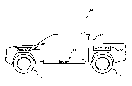
Referring now to FIGURES lA and 1B and given by way of overview, in various
embodiments an electric vehicle 10 includes a vehicle body 12. A high voltage
direct
current (DC) electrical battery 14 is disposed within the vehicle body 12.
Left and right
front wheels 16 (only the left front wheel 16 is shown) and left and right
rear wheels 18
(only the left rear wheel 18 is shown) are configured to rotate. At least one
drive unit 20
is mechanically couplable to rotate the front wheels 16 or the rear wheels 18
(and in some
embodiments one drive unit 20 may be mechanically couplable to rotate the
front wheels
16 and another drive unit 20 may be mechanically couplable to rotate the rear
wheels 18).
Each drive unit 20 is electrically connectable to receive high voltage DC
electrical power
from the battery 14. Each drive unit 20 includes axles 22A and 22B that are
mechanically
couplable to rotate an associated wheel 16 or 18 and electrical motors 24A and
24B
mechanically couplable to rotate its associated axle 22A and 22B,
respectively. As will be
6
Date Recue/Date Received 2022-01-11
explained below, each drive unit 20 also includes a dual power inverter module
26 that is
electrically connectable to receive the high voltage DC electrical power from
the battery
14. The dual power inverter module 26 includes two inverters (not shown)
configured to
create three-phase, high voltage alternating current (AC) electrical power
from the high
voltage DC electrical power and provide the three-phase, high voltage AC
electrical power
to an associated electrical motor. A common controller (not shown) is
configured to
control both of the inverters in the dual power inverter module 26.
For sake of brevity, illustrative details are set forth below by way of non-
limiting
examples in the context of a motor vehicle. However, it will be appreciated
that the vehicle
can be any type of vehicle whatsoever as desired without limitation. Given by
way of
non-limiting example, in various embodiments the vehicle 10 may be an electric
vehicle
(that is, an all-electrically driven vehicle) or a hybrid vehicle. For example
and given by
way of non-limiting examples, in various embodiments the vehicle 10 may
include a motor
vehicle driven by wheels and/or tracks, such as, without limitation, an
automobile, a truck,
a sport utility vehicle (SUV), a van, an all-terrain vehicle (ATV), a
motorcycle, an electric
bicycle, a tractor, a lawn mower such as without limitation a riding lawn
mower, a
snowmobile, and the like. Given by way of further non-limiting examples, in
various
embodiments the vehicle 10 may include a marine vessel such as, without
limitation, a
boat, a ship, a submarine, a submersible, an autonomous underwater vehicle
(AUV), and
the like. Given by way of further non-limiting examples, in various
embodiments the
vehicle 10 may include an aircraft such as, without limitation, a fixed wing
aircraft, a rotary
wing aircraft, and a lighter-than-air (LTA) craft.
7
Date Recue/Date Received 2022-01-11
Also for sake of brevity, illustrative details regarding the drive unit 20 are
set forth
in the context of a motor vehicle. Because the vehicle 10 is not limited to
the illustrative
example of a motor vehicle, it will be appreciated that the drive unit 20 also
is not limited
to applicability to a motor vehicle. To that end, in various embodiments the
motor (or
motors) of the drive unit 20 are configured to drive the vehicle 10. That is,
in various
embodiments the electric motor (or motors) of the drive unit 20 may drive any
drive
member that drives any propulsion device, such as without limitation a wheel
or wheels, a
track or tracks, a propellor or propellors, a propulsor or propulsors, a rotor
or rotors, or the
like, associated with the vehicle 10.
For example, in some embodiments in a motor vehicle one drive unit 20 may
include
one motor configured to drive one drive member such as an axle or a chain ring
that drives
one wheel or track, in some other embodiments in a motor vehicle one drive
unit 20 may
include one motor configured to drive an axle that rotates two wheels or two
tracks, and in
some other embodiments in a motor vehicle one drive unit 20 may include one
motor
configured to drive an axle that rotates one wheel or one track and another
motor
configured to drive another axle that rotates another wheel or another track.
Similarly, in some embodiments in a marine vessel one drive unit 20 may
include
one motor configured to drive one propeller or propulsor, in some other
embodiments in a
marine vessel one drive unit 20 may include one motor configured to drive a
shaft that
rotates two propellers or two propulsors, and in some other embodiments in a
marine vessel
one drive unit 20 may include one motor configured to drive a shaft that
rotates one
8
Date Recue/Date Received 2022-01-11
propeller or propulsor and another motor configured to drive another shaft
that rotates
another propeller or propulsor.
Likewise, in some embodiments in an aircraft one drive unit 20 may include one
motor configured to drive one propeller or rotor, in some other embodiments in
an aircraft
one drive unit 20 may include one motor configured to drive a shaft that
rotates two
propellers or two rotors, and in some other embodiments in an aircraft one
drive unit 20
may include one motor configured to drive a shaft that rotates one propeller
or rotor and
another motor configured to drive another shaft that rotates another propeller
or rotor.
Now that an overview has been set forth, illustrative details will be
explained with
examples that are given by way of illustration only and not of limitation.
As mentioned above, the at least one drive unit 20 is mechanically couplable
to
rotate the front wheels 16 or the rear wheels 18 (and in some embodiments one
drive unit
20 may be mechanically couplable to rotate the front wheels 16 and another
drive unit 20
may be mechanically couplable to rotate the rear wheels 18). As also mentioned
above,
each drive unit 20 includes the axles 22A and 22B that are mechanically
couplable to rotate
an associated wheel 16 or 18 and electrical motors 24A and 24B that are
mechanically
couplable to rotate its associated axle 22A and 22B, respectively.
Referring additionally to FIGURES 2A-2E, in various embodiments each
electrical
motor 24A and 24B is mechanically couplable to rotate its associated axle 22A
and 22B,
respectively, via a set of gears 28A and 28B, respectively. Each set of gears
28A and 28B
is configured to provide speed and torque conversions from its associated
electrical motor
9
Date Recue/Date Received 2022-01-11
24A or 24B, respectively, to its associated axle 22A or 22B, respectively,
and, ultimately,
an associated wheel 16 or 18.
As shown in FIGURE 2D, a shaft 21A is configured to be rotated by its
associated
rotor 27 of its electrical motor 24A and a shaft 21B is configured to be
rotated by its
associated rotor 27 of its electrical motor 24B. The shafts 21A and 21B are
supported and
constrained within bearings (not shown) disposed on a frame 19. The set of
gears 28A is
disposed within the frame 19 and is configured to rotatably engage the axle
22A and the
set of gears 28B is disposed within the frame 19 and is configured to
rotatably engage the
axle 22B. The electrical motor 24A is configured to rotatably engage the set
of gears 28A
and the electrical motor 24B is configured to rotatably engage the set of
gears 28B.
In various embodiments, each of the sets of gears 28A and 28B is configured to
provide speed and torque conversions from its associated electrical motor 24A
or 24B to
its associated axle 22A or 22B and, ultimately, an associated wheel 16 or 18.
For example
and given by way of illustration only and not of limitation, in various
embodiments a gear
28C is configured to be rotated by its associated shaft 21A or 21B. A gear 28D
is mounted
on a shaft (not shown for purposes of clarity) and is configured to be
meshedly engaged by
the gear 28C. A gear 28E also is mounted on the shaft (not shown for purposes
of clarity).
A gear 28F is mounted on the axle 22A or 22B and is configured to be meshedly
engaged
by the gear 28E. It will be appreciated that, in various embodiments, the sets
of gears 28A
and 28B may include any number of suitable gears (such as, without limitation,
planetary
gears) with gear ratios selected as desired for a particular application to
achieve desired
speed and torque conversions. It will be appreciated that gears for use in
electric vehicles
Date Recue/Date Received 2022-01-11
are well known in the art. Therefore, further description of their
construction and operation
are not necessary for an understanding of disclosed subject matter.
In some embodiments, the axles 22A and 22B may be fixedly couplable to their
associated wheels 16 or 18. For example and without limitation, in some such
embodiments the front wheels 16 may be fixedly couplable to their associated
axles 22A
and 22B. It will be appreciated that such fixed coupling may help contribute
to reducing
mechanical complexity and may help contribute to enabling the front wheels 16
to remain
steerable (such as when the vehicle 10 is being towed with the front wheels 16
and the rear
wheels 18 engaged on a surface of a road (that is, flat towing)).
In some other embodiments, the axles 22A and 22B may be removably couplable
to their associated wheels 16 or 18. For example and without limitation, in
some such
embodiments the rear wheels 18 may be removably couplable to their associated
axles 22A
and 22B. It will be appreciated that such removable coupling of the rear
wheels 18 may
help contribute to avoiding generation of braking torque and/or uncontrolled
electrical
generation during towing.
It will be appreciated that each drive unit 20 drives either left and right
front wheels
16 or left and right rear wheels 18. Therefore, both of the electrical motors
24A and 24B
of a given drive unit 20 may experience a same or similar range of speed and
torque
demands. To service such ranges of speed and torque demands, in various
embodiments
both of the electrical motors 24A and 24B of a given drive unit 20 may have
the same
voltage and current ratings. For example, in various embodiments (such as in
high voltage
systems), a voltage rating may be in a range from around 300Vrms to around
600Vrms
11
Date Recue/Date Received 2022-01-11
line-to-line and a current rating may be in a range from around 300 Arms to
around 900
Arms. Given by way of non-limiting example by way of illustration only, an
illustrative
voltage rating may be 312 Vrms and an illustrative current rating may be 550
Arms (based
on a 400VDC system). However, it will be appreciated that the electrical
motors 24A and
24B may have any voltage ratings and any current ratings as desired for a
particular
application.
In various embodiments, the electrical motors 24A and 24B may be any suitable
type of electrical motor as desired. For example, in some embodiments the
electrical
motors 24A and 24B may include synchronous electrical motors. In some such
embodiments, the synchronous electrical motors may include without limitation
permanent
magnet electrical motors or the like. In some other embodiments the electrical
motors 24A
and 24B may include without limitation an asynchronous motor (or induction
motor) ¨ like
a polyphase AC induction motor or the like.
As mentioned above, in various embodiments each drive unit 20 drives either
left
and right front wheels 16 or left and right rear wheels 18 and, therefore,
both of the
electrical motors 24A and 24B of a given drive unit 20 may experience a same
or similar
range of speed and torque demands. Therefore, in various embodiments both
inverters of
a given drive unit 20 may have the same voltage output ratings and the same
current output
ratings. Given by way of illustration only and not of limitation, in various
embodiments
both inverters of a given drive unit 20 may have a voltage output rating of
312Vrms and a
current output rating of 550Arms (based on 400VDC input). However, it will be
12
Date Recue/Date Received 2022-01-11
appreciated that the inverters of a given drive unit 20 may have any voltage
output ratings
and any current output ratings as desired for a particular application.
It will be appreciated that, in various embodiments, the dual power inverter
module
26 may be physically associated with the frame 19 in any suitable manner as
desired for a
particular application. For example and without limitation, in some
embodiments and as
shown in FIGS. 2A-2C the dual power inverter module 26 may be a module within
a sealed
container and physically disposed on the frame 19 external to the frame. As
another
example and as shown in FIGURE 2E without limitation, in some other
embodiments the
dual power inverter module 26 may be integratably mountable with the frame 19.
In some
such embodiments a housing 29 has an open face (not shown) defined therein.
Inverter
circuitry (discussed below) is disposed in the housing 29. In such
embodiments, the open
face of the housing 29 is mated to an opening (not shown) in the frame 19.
Such other
embodiments are discussed in commonly-owned U.S. Patent Application Ser. No.
17/244,288 filed April 29, 2021 entitled "INVERTER MODULE INTEGRATABLY
MOUNTABLE WITH DRIVE UNIT OF VEHICLE" assigned to and filed by Applicant,
the entire contents of which are hereby incorporated by reference.
Referring additionally to FIGURES 3A and 3B, in various embodiments a dual
power inverter module (DPIM) 26 is provided. As mentioned above, in various
embodiments the DPIM 26 includes two inverters 30A and 30B configured to
create three-
phase, high voltage AC electrical power from the high voltage DC electrical
power and
provide the three-phase, high voltage AC electrical power to an associated
electrical motor
13
Date Recue/Date Received 2022-01-11
24A or 24B and a common controller 32 configured to control both of the
inverters 30A
and 30B.
In various embodiments, a DC link capacitor 34 is electrically connectable to
a
source of high voltage DC electrical power, such as the battery 14. In some
embodiments,
an electrical connection to the battery 14 may include an electrical
connection 36. Suitable
electrical cables 38 may be electrically connected to the electrical
connection 36 and may
be electrically connectable to the electrical battery 14.
In various embodiments, a power inverter 30A is electrically connectable to
the DC
link capacitor 34 and is configured to convert high voltage DC electrical
power to three
phase high voltage AC electrical power. The power inverter 30A is further
configured to
supply the three phase high voltage AC electrical power to an electric motor
24A, such as
a right motor or a left motor. A power inverter 30B is electrically
connectable to the DC
link capacitor 34 and configured to convert high voltage DC electrical power
to three phase
high voltage AC electrical power. The power inverter 30B is further configured
to supply
the three phase high voltage AC electrical power to an electric motor 24B,
such as the other
of the left motor or right motor.
In various embodiments the common controller 32 is electrically connectable to
the
power inverter 30A and the power inverter 30B. The common controller 32 is
configured
to control the power inverter 30A and the power inverter 30B. The common
controller 32
may be any suitable computer processor-based controller as desired. Given by
way of
example only and not of limitation, in various embodiments the common
controller 32 may
include a computer processing unit (CPU), a general purpose processor, a
digital signal
14
Date Recue/Date Received 2022-01-11
processor, a field programmable gate array, or the like, and/or any
combination thereof
While controllers are well known and further description of their construction
and
operation are not necessary for an understanding of disclosed subject matter,
further details
regarding the common controller 32 will be set forth below regarding
additional functions.
In various embodiments, the common controller 32 is electrically connectable
to
receive low voltage DC electrical power, such as 12 VDC. The common controller
32 also
is electrically connectable to receive vehicle status signals and vehicle
fault indication
signals. Illustrative responses to various vehicle faults and to loss of 12
VDC will be
discussed further below.
In various embodiments, the power inverter 30A and the power inverter 30B each
include a bank 40 of three-terminal power semiconductor devices 42 and a bank
44 of the
three-terminal power semiconductor devices 42.
In some embodiments, the three-terminal power semiconductor devices 42 may
include insulated gate bipolar transistors (IGBTs). In some such embodiments,
the IGBTs
may include silicon (Si) IGBTs. In some embodiments, the three-terminal power
semiconductor devices 42 may include metal-oxide-semiconductor field effect
transistors
(MOSFETs). In some such embodiments, the MOSFETs may include silicon carbide
(SiC)
MOSFETs. However, it will be appreciated that the three-terminal power
semiconductor
devices 42 may also include power semiconductor devices 42 that include at
least three
terminals and may include additional terminals ¨ such as, for example and
without
limitation, Kelvin source terminal, Kelvin emitter terminal, current sense
terminal, and/or
temperature sense terminal.
Date Recue/Date Received 2022-01-11
It will be appreciated that SiC MOSFETS may offer advantages over Si IGBTs at
low phase currents and that SiC MOSFETS have lower conduction drop compared to
IGBTs below 700 Apk. However, it will be appreciated that this value may
change
depending upon size of the inverter. As such, it will be appreciated that SiC
MOSFETS
may offer up to around 3-5% efficiency gains over a typical drive cycle, as
compared to Si
IGBTs.
In some all-wheel drive (AWD) electric vehicles 10, the front wheels 16
function as
the only drive wheels until additional torque and/or power beyond a
predetermined amount
is entailed. In such electric vehicles 10, the rear wheels are only driven by
their associated
drive unit 20 when torque and/or power beyond the predetermined amount is to
be
delivered. In some such AWD electric vehicles 10, to take advantage of
efficiencies of
SiC MOSFETS over Si IGBTs the drive unit 20 that drives the front wheels 16
may include
inverters 40 that include SiC MOSFETS and the drive unit 20 that drives the
rear wheels
18 may include inverters 40 that include Si IGBTs. However, it will be
appreciated that
any of the drive units 20 may include inverters 40 that include either SiC
MOSFETS or Si
IGBTs as desired.
In various embodiments the power inverter 30A includes a gate drive circuit
46A
configured to drive gate terminals 48 of the banks 40 and 44 of three-terminal
power
semiconductor devices 42 of the power inverter 30A. Similarly, the power
inverter 30B
includes a gate drive circuit 46B configured to drive gate terminals 48 of the
banks 40 and
44 of three-terminal power semiconductor devices 42 of the power inverter 30B.
In various
embodiments the controller 32 is configured to, among other functions,
generate low-
16
Date Recue/Date Received 2022-01-11
power turn on and turn off signals 66A and 66B and provide the turn on and
turn off signals
66A and 66B to the gate drive circuits 46A and 46B, respectively. The low-
power turn on
and turn off signals 66A and 66B may be on the order of a few milliamperes of
electrical
current and logic level voltages such as 3.3 or 5V.
In various embodiments the gate drive circuits 46A and 46B include suitable
power
amplifiers that amplify the low-power turn on and turn off signals 66A and 66B
and
generate high-power turn on and turn off signals 66A' and 66B'. To drive the
gate
terminals 48, the high-power turn on and turn off signals 66A' and 66B' may be
on the
order of several hundreds of milliamperes of electrical current or on the
order of amperes
of electrical current, with voltages in the range of 15-20V, as desired for a
particular
application. The high-power turn on and turn off signals 66A' and 66B' are, in
turn,
electrically coupled to drive associated gate terminals 48. Gate drive
circuits are well
known and further description of their construction and operation are not
necessary for an
understanding of disclosed subject matter.
In view of the illustrative details provided above by way of non-limiting
examples,
it will be appreciated that, in various embodiments, provision of one
controller 32 for two
inverters 30A and 30B can provide for use of: (i) a single interface for
vehicle status signals
and vehicle fault indication signals; (ii) a single DC link capacitor 34;
(iii) a single common
controller 32; and (iv) a single interface for low voltage DC electrical power
(such as 12
VDC).
In view of the illustrative details provided above by way of non-limiting
examples,
it will be appreciated that, in various embodiments, integrating the mounting
of the DPIM
17
Date Recue/Date Received 2022-01-11
26 with the drive unit 20 can provide for integration of coolant interfaces.
For example, in
various embodiments water cooling provided for the inverters 30A and 30B can
be
provided to stator windings of the electrical motors 24A and 24B.
As discussed above, in various embodiments a single motor 24A or 24B drives a
single wheel, such as one front wheel 16 or one rear wheel 18. It will be
appreciated that
each wheel can operate at a unique speed and torque. Given by way of non-
limiting
examples, going around a curve or loss of traction can create different wheel
speeds and
traction control or torque vectoring can result in different wheel torques. As
also discussed
above, in various embodiments the dual power inverter module 26 combines two
inverters
30A and 30B into one module 26 and, as such, shares common components, such as
the
DC link capacitor 34.
To that end, various embodiments include only one DC link capacitor 34 that is
electrically connectable to provide high voltage DC electrical power to both
inverters 30A
and 30B of the DPIM 26. It will be appreciated that it may be desirable to
reduce and
possibly minimize size of the DC link capacitor 34. As explained below,
various
embodiments can help contribute to reducing stress on the DC link capacitor 34
(that may
have a reduced size) and ripple current on the DC high voltage bus (that may
include the
electrical cables 38) due to generation fof high-frequency current harmonics
from the
inverters 30A and 30B.
In various embodiments, the inverters 30A and 30B use pulse width modulation
(PWM) to create a variable amplitude and frequency voltage source to drive the
electric
motors 24A and 24B. Different PWM methods (such as, for example, continuous
PWM
18
Date Recue/Date Received 2022-01-11
and discontinuous PWM) can be employed as desired for a particular situation.
Each of
the PWM methods creates its own unique harmonic spectrum of ripple current
that may be
reflected on the DC bus.
For example, in continuous PWM each phase is switching continuously (that is,
in
various embodiments all of the three-terminal power semiconductor devices 42
in both of
the inverters 30A and 30B are switching continuously). As a result, continuous
PWM can
result in a not-insignificant amount of switching losses in the inverters 30A
and 30B. In
continuous PWM, the second harmonic of the switching frequency is the dominant
harmonic frequency in the ripple current. Continuous PWM (such as space vector
modulation) can be used in situations such as when it is desired to minimize
harmonic
content and ripple on AC output and DC input currents, as well as minimize
acoustic noise.
For example, some vehicles might use continuous PWM at high torque to minimize
acoustic noise.
As another example, in discontinuous PWM each phase is not switching
continuously (that is, in various embodiments all of the three-terminal power
semiconductor devices 42 in both of the inverters 30A and 30B are not
switching
continuously). In such embodiments, only two of the three phases are switching
at any one
time, and the remaining third phase has either the upper or lower switch
turned on
continuously, thereby helping to contribute to increasing inverter efficiency
and helping to
contribute to reducing losses during discontinuous PWM. It will be appreciated
that use
of discontinuous PWM may have other non-beneficial effects, such as increased
acoustic
noise or harmonic content in the AC output or DC input currents. In
discontinuous PWM
19
Date Recue/Date Received 2022-01-11
each phase has two 60 degree segments where the switches are held either low
or high, and
is not switching for a total of 120 degrees over a fundamental period. That
is, in
discontinuous PWM each phase is not switching one-third of the time. This
results in
significantly lower switching losses and higher efficiency. It will be
appreciated that, while
discontinuous PWM entails lower switching losses than those entailed in
continuous PWM,
discontinuous PWM may entail higher acoustic noise than that associated with
continuous
PWM and harmonics may be placed onto the motors 24A and 24B as well as the DC
link
capacitor 34. In discontinuous PWM, the first harmonic of the switching
frequency is the
dominant harmonic frequency. Discontinuous PWM can be used in situations when
the
highest efficiency and lowest losses are desired, and acoustic noise is not
problematic. As
an example, some vehicles might have thermal problems at high torque and, as a
result, use
discontinuous PWM to reduce losses under those conditions.
In various embodiments and referring additionally to FIGURE 4A, the DC link
capacitor 34 is used to decouple effects of inductance Lcable from the DC
voltage source
(that is, the electrical battery 14) to the inverters 30A and 30B. Referring
additionally to
FIGURES 4B and 4C, the DC link capacitor 34 provides a low impedance path for
ripple
currents 50 that are generated by the inverters 30A and 30B and might
otherwise flow back
onto the DC high voltage bus. The ripple currents 50 are a factor in sizing
the DC link
capacitor 34 and, as a result, reducing the ripple currents 50 can help
contribute to reducing
size of the DC link capacitor 34 (and stress on the DC link capacitor 34). The
ripple
currents 50 are a result of the AC load current flowing into the motors 24A
and 24B and
pulse width modulation (PWM) of the inverters 30A and 30B. As shown in FIGURES
4B
Date Recue/Date Received 2022-01-11
and 4C and given by way of illustration only and not of limitation, with a
motor current of
550 Arms, a modulation index of 0.48, a power factor of 1, a switching
frequency of 10
KHz, and a fundamental frequency of 250 Hz, without cancellation the ripple
currents 50
can have an amplitude of around 712 Arms.
Referring additionally to FIGURE 4D, in various embodiments a method 52 is
provided for synchronizing pulse width modulation clocks. It will be
appreciated that, in
various embodiments, synchronizing pulse width modulation clocks can help
contribute to
cancelling the ripple currents 50. The method 52 begins at a block 53. At a
block 54 a
pulse width modulation method of a first power inverter and a pulse width
modulation
method of a second power inverter are identified. At a block 56, a switching
frequency of
the first power inverter and a switching frequency of the second power
inverter are
identified and compared. At a block 58, an optimized phase shift between the
first power
inverter and the second power inverter is determined responsive to the pulse
width
modulation method of the first power inverter and the pulse width modulation
method of
the second power inverter and the switching frequency of the first power
inverter and the
switching frequency of the second power inverter. At a block 60 the optimized
phase shift
is synchronized between the first power inverter and the second power
inverter.
The method 52 ends at a block 61.
As shown in FIGURES 4E and 4F and given by way of illustration only and not of
limitation, with a motor current of 550 Arms, a modulation index of 0.48, a
power factor
of 1, a switching frequency of 10 KHz, and a fundamental frequency of 250 Hz,
with
21
Date Recue/Date Received 2022-01-11
cancellation as described herein the ripple currents 50 can be reduced to have
an amplitude
of around 147 Arms.
With the above overview in mind, in various embodiments and as shown in
FIGURE 3A the common controller 32 includes a processor 64A and a processor
64B. In
some embodiments the processors 64A and 64B may be separate processors.
However, it
will be appreciated that in some other embodiments (that use two PWM
generators) the
functions of the processors 64A and 64B may be combined into a single
processor as
desired for a particular application. Regardless of the processors 64A and 64B
being
separate or combined into a single processor, it will be appreciated that the
processor 64A
functions as a Master and the processor 64B functions as a Slave.
The processor 64A is operably coupled to computer-readable media 65A, such as
any suitable computer memory, configured to store computer-executable
instructions
configured to cause the processor 64A to perform functions described below.
The
processor 64B is operably coupled to computer-readable media 65B, such as any
suitable
computer memory, configured to store computer-executable instructions
configured to
cause the processor 64B to perform functions described below. The processor
64A is
configured to generate a first clock signal (e.g., using a crystal) for
controlling generation
of the turn on and turn off signal 66A for driving the power inverter 30A and
a second
clock signal. The second clock signal is provided to the processor 64B for
controlling
generation of the turn on and turn off signal 66B for driving the power
inverter 30B.
The processor 64A selects a PWM method for the power inverter 30A and the
processor 64B selects a PWM method for the power inverter 30B. The processor
64B (that
22
Date Recue/Date Received 2022-01-11
is, the Slave) informs the processor 64A (that is, the Master) of its PWM
method (except
for cases where switching of PWM methods is not employed). Factors for
selection of
continuous PWM and discontinuous PWM have been discussed above.
The processor 64A selects a switching frequency for the power inverter 30A and
the
processor 64B selects a switching frequency for the power inverter 30B. The
frequencies
are even multiples of each other, and are selected from predetermined values.
Given by
way of illustration only and not of limitation, in various embodiments the
switching
frequencies may be 2.5KHz and 10KHz, thereby resulting in an even multiple of
four.
However, it will be appreciated that other frequencies may be selected as
desired (that
result in even multiples). In various embodiments the processor 64A (that is,
the Master)
puts out a reference that is at the lowest selectable frequency, with the
desired phase shift
as a function of the PWM modes.
The processor 64A is configured to determine an optimized phase shift between
the
power inverter 30A and the power inverter 30B responsive to the PWM method of
the
power inverter 30A and the PWM method of the power inverter 30B and the
switching
frequency of the power inverter 30A and the switching frequency of the power
inverter
30B. For example, in some such embodiments and referring additionally to
FIGURE 4G,
the processor 64A may access a look-up-table 68 that is populated with cells
that include
values of optimized phase shift arranged according to rows 70 of PWM method
and
columns 72 of PWM method. It will be appreciated that, in some embodiments,
the PWM
method of the power inverter 30A and the PWM method of the power inverter 30B
may
be the same pulse width modulation method. It will also be appreciated that,
in some other
23
Date Recue/Date Received 2022-01-11
embodiments, the PWM method of the power inverter 30A and the PWM method of
the
power inverter 30B may be different PWM methods.
As shown in FIGURE 4G, when both of the power inverters 30A and 30B use
continuous PWM, the phase shift is set to 90 degrees. When both of the power
inverters
30 A and 30B use discontinuous PWM, the phase shift is set to 180 degrees. In
the event
of different PWM methods, the phase is set to 90 degrees.
In some other such embodiments, the processor 64A may execute an algorithm for
determining an optimized phase shift between the power inverter 30A and the
power
inverter 30B responsive to the PWM method of the power inverter 30A and the
PWM
method of the power inverter 30B. For example, the algorithm may include if-
then
statements, such as:
if both PWM methods are continuous PWM, then the optimized phase shift is 90
degrees;
if both PWM methods are discontinuous PWM, then the optimized phase shift is
180 degrees; and
if one PWM method is continuous PWM and another PWM method is discontinuous
PWM, then the optimized phase shift is 90 degrees.
The processor 64A is also configured to synchronize the optimized phase shift
between the power inverter 30A and the power inverter 30B. As mentioned above,
the
processor 64B is configured to receive the second clock signal and to drive
the power
inverter 30B.
24
Date Recue/Date Received 2022-01-11
In various embodiments, the processor 64A is further configured to shift the
second
clock signal from the first clock signal by the determined optimized phase
shift.
In various embodiments, the processor 64A is further configured to identify a
dominant harmonic frequency among harmonic frequencies of the PWM method of
the
power inverter 30A and the PWM method of the power inverter 30B and to
determine the
optimized phase shift between the power inverter 30A and the power inverter
30B
responsive to the dominant harmonic frequency among the harmonic frequencies
of the
PWM method of the power inverter 30A and the PWM method of the power inverter
30B.
It will be appreciated that determining the optimized phase shift between the
power inverter
30A and the power inverter 30B responsive to the dominant harmonic frequency
among
the harmonic frequencies of the PWM method of the power inverter 30A and the
PWM
method of the power inverter 30B can help contribute to cancelling dominant
high
frequency components of the ripple currents 50.
In some such embodiments, the dominant harmonic frequency may include a second
harmonic frequency (harmonic of the switching frequency). For example, in such
embodiments the PWM method may include continuous PWM. In such embodiments,
the
optimized phase shift is 90 degrees. It will be appreciated that a phase shift
of 90 degrees
shifts the dominant harmonic (second harmonic frequency) by 180 degrees,
thereby
resulting in cancellation of the dominant harmonic component of the ripple
current 50.
In some other such embodiments, the dominant harmonic frequency may include a
first harmonic frequency. For example, in such embodiments the PWM method may
include discontinuous PWM. In such embodiments, the optimized phase shift is
180
Date Recue/Date Received 2022-01-11
degrees. It will be appreciated that a phase shift of 180 degrees shifts the
dominant
harmonic (first harmonic frequency) by 180 degrees, thereby resulting in
cancellation of
the dominant harmonic component of the ripple current 50.
It will be appreciated that actual DC bus harmonics may reside in side band
groups
surrounding the switching frequency. The separation of these harmonics from
the
switching frequency harmonic is a function of the motor fundamental frequency.
In various embodiments the processor 64A is configured to identify and compare
a
switching frequency of the power inverter 30A and a switching frequency of the
power
inverter 30B. As discussed above, only two frequencies that are even multiples
of each
other are used.
For example, in some embodiments it may be desirable to change switching
frequency. For example, in some embodiments switching frequency may be 10 KHz.
In
such embodiments, at low motor speed (for example, below 500 RPM) it may be
desirable
to reduce switching frequency to 2.5KHz to protect the switches 42 in the
inverters 30A
and 30B, thereby helping to reduce stresses in the inverters 30A and 30B.
Maintaining
even multiple relation between the switching frequencies allows for alignment
of
harmonics and increased opportunity for cancellation of dominant harmonics.
Electric vehicles in which each wheel is independently driven by its own
associated
electrical motor via its own axle does not have any mechanical coupling
between the
wheels. In such vehicles, if one inverter shuts down due to a fault and the
other inverter
does not react appropriately, then a torque difference might exist between the
two wheels.
26
Date Recue/Date Received 2022-01-11
Such a resultant torque difference might have negative impact on
controllability of the
vehicle.
To help avoid such a torque difference and referring additionally to Figures
5A-5G,
in various embodiments a fault that is associated with either the power
inverter 30A or the
power inverter 30B (or circuitry described below that is associated with both
the inverters
30A and 30B) results in application of a same fault action (described below)
to both the
inverters 30A and 30B. In such embodiments, application of the same fault
action to both
the inverters 30A and 30B puts both the inverters 30A and 30B in a "safe
state" and helps
contribute to applying an equalized torque to both of the wheels associated
with the drive
unit 20 that includes the inverters 30A and 30B. By applying the same fault
action to both
the inverters 30A and 30B and equalizing torque to both of the wheels
associated with the
drive unit 20 that includes the inverters 30A and 30B, various embodiments are
able to
help contribute to reducing the possibility of generation of torque difference
that might
have negative impact on controllability of the vehicle.
As discussed above, the processor 64A is operably coupled to computer-readable
media 65A, such as any suitable computer memory, configured to store computer-
executable instructions configured to cause the processor 64A to perform
functions
described below. As also discussed above, the processor 64B is operably
coupled to
computer-readable media 65B, such as any suitable computer memory, configured
to store
computer-executable instructions configured to cause the processor 64B to
perform
functions described below. In various embodiments and as will be described
below, the
computer-executable instructions are configured to cause its associated
processor 64A and
27
Date Recue/Date Received 2022-01-11
64B to apply a same fault action to the power inverter 30A and the power
inverter 30B,
respectively, for applying equalized torque to each wheel 16 or 18 operatively
coupled to
the drive unit 20 responsive to a fault associated with the power inverter 30A
or the power
inverter 30B
In various embodiments and as shown in FIGURE 5A, various faults associated
with the inverters 30A and 30B are monitored by the processors 64A and 64B for
the
inverters 30A and 30B, respectively. For such faults, in various embodiments
the same
fault response is applied by the processors 64A and 64B to the three-terminal
power
semiconductor devices 42 (FIGURE 3A) of both of the inverters 30A and 30B. In
various
embodiments, such faults associated with the inverters 30A and 30B and
monitored by the
processors 64A and 64B, respectively, may include, without limitation,
overcurrent,
overvoltage, undervoltage, over temperature, overspeed, and the like. In
various
embodiments, signals indicative of such faults may be provided to the
controller 32 via a
data link 74 that may include any suitable data communication connection or
network as
desired, such as without limitation a wide area network (WAN), a local area
network
(LAN), a controller area network (CAN), a peer-to-peer network, a data bus, or
the like
and provided to the processors 64A and 64B. In various embodiments, signals
indicative
of vehicle status, such as motor speed and voltage of the battery 14, are also
provided to
the controller 32 via the data link 74.
In various embodiments and as also shown in FIGURE 5A, the controller 32
includes a communications link 82 between the processors 64A and 64B.
It will be
appreciated that the communications link 82 can enable the processor 64A or
the processor
28
Date Recue/Date Received 2022-01-11
64B to communicate to the other processor 64B or 64A, respectively, that a
fault monitored
by the processor 64A or the processor 64B has been detected, that a fault
action is to be
taken, and what fault action is to be taken. The communications link 82 may
include any
suitable data link or data bus as desired.
In various embodiments, the fault action for a fault monitored by the
processors 64A
and 64B for the inverters 30A and 30B, respectively, may include an action
such as opening
all of the three-terminal semiconductor devices 42 of the inverters 30A and
30B and/or
shorting the three-terminal semiconductor devices 42 of either the bank 40 or
the bank 44
of the inverters 30A and 30B. As will be explained below, in various
embodiments the
fault action applied to both of the inverters 30A and 30B for a fault
monitored by the
processors 64A and 64B depends on speed of the motors. As will also be
explained below,
the fault action applied to both of the inverters 30A and 30B for a fault that
is not monitored
by the processors 64A and 64B does not depend on speed of the motors.
In various embodiments and as mentioned above, in various embodiments the
fault
action for a fault monitored by the processors 64A and 64B for the inverters
30A and 30B,
respectively, may include an action such as opening all of the three-terminal
semiconductor
devices 42 of the inverters 30A and 30B and/or shorting the three-terminal
semiconductor
devices 42 of either the bank 40 or the bank 44 of the inverters 30A and 30B
and may
depend on speed of the motors. For such faults that are monitored by the
processors 64A
and 64B, it will be appreciated that the fault action applied to both of the
inverters 30A and
30B simultaneously can help contribute to reducing braking torque and reducing
regenerative electrical current to the electrical battery 14. Because the
processors 64A and
29
Date Recue/Date Received 2022-01-11
64B are operatively coupled to various data communication connections or
networks to
receive data regarding speed of the motors, the processors 64A and 64B
suitably are
configured to determine the same fault action to be applied based on speed of
the motors.
In various embodiments, the processor 64A selects the appropriate speed-
dependent fault
action for its associated electrical motor 24A and the processor 64B selects
the appropriate
speed-dependent fault action for its associated electrical motor 24B. Fault
actions for other
faults ¨ that are not monitored by the processors 64A and 64B ¨ do not depend
on speed
of the motors and are discussed further below.
As shown in FIGURE 5B, in various embodiments the same fault action to be
applied the inverters 30A and 30B may be based on speed of the motors. In such
embodiments the same fault action may include opening all of the three-
terminal
semiconductor devices 42 of the inverters 30A and 30B below a threshold speed
viii of the
motor and shorting the three-terminal semiconductor devices 42 of either the
bank 40 or
the bank 44 of the inverters 30A and 30B above the threshold speed viii.
As shown in FIGURE 5B, a graph 76 plots speed of the motor versus torque for
various conditions of the three-terminal semiconductor devices 42 of the
inverters 30A and
30B. A curve 78 shows torque that results from opening all of the three-
terminal
semiconductor devices 42 of the inverters 30A and 30B. Below the threshold
speed vth
torque is substantially insignificant and above the threshold speed viii
braking torque
becomes increasingly significant with increased speed of the motors. It will
also be
appreciated that, in such instances, back electromotive force (back EMF)
increases with
increasing speed of the motors which can, in some instances, result in the
electrical motors
Date Recue/Date Received 2022-01-11
24A and 24B possibly operating as uncontrolled generators that can generate
back EMF
and apply unwanted regenerated electrical current to the DC link capacitor 34
and the
electrical battery 14.
As also shown in FIGURE 5B, a curve 80 shows torque that results from a three-
phase short of the three-terminal semiconductor devices 42 of either the bank
40 or the
bank 44 of three-terminal semiconductor devices 42. As speed of the motors
increases
from zero, braking torque rapidly increases and reaches a maximum value of
braking
torque. As speed of the motors continues to increase, braking torque decreases
and
approaches an asymptotic minimized value before the speed of the motors
reaches the
threshold speed viii.
Thus, in various embodiments in which the fault is monitored by the processors
64A
and 64B for the inverters 30A and 30B, the fault action suitably includes a
speed-dependent
fault action that can help contribute to simultaneously minimize braking
torque and
unwanted regenerative electrical current to the DC link capacitor 34 and the
electrical
battery 14. In such embodiments, the fault action suitably includes opening
all of the three-
terminal power semiconductor devices 42 of both of the inverters 30A and 30B
when the
speed of the motors is less than the threshold speed vth and shorting the
three-terminal
power semiconductor devices 42 of one bank of the three-terminal power
semiconductor
devices 42 (that is, either the bank 40 or the bank 44) of the inverters 30A
and 30B when
the speed of the motors is greater than the threshold speed Vth.
In various embodiments, fault actions based on the curve 78 and the graph 80
may
be implemented using back EMF and voltage of the battery 14 (as opposed to
taking fault
31
Date Recue/Date Received 2022-01-11
action directly in response to reported motor speed). For example, in various
embodiments
motor back EMF is computed and is compared to voltage of the battery. In such
embodiments, when back EMF is less than battery voltage (by a design safety
margin
selected as desired), then a speed-dependent fault action includes opening all
of the three-
terminal power semiconductor devices 42 of both of the inverters 30A and 30B.
When
back EMF exceeds a predetermined percentage of battery voltage, then a speed-
dependent
fault action includes shorting the three-terminal power semiconductor devices
42 of one
bank of the three-terminal power semiconductor devices 42 (that is, either the
bank 40 or
the bank 44) of the inverters 30A and 30B. If desired, use of an amount of
hysteresis can
prevent "chattering" back-and-forth between different fault actions.
As shown in FIGURE 5A, the processor 64A is associated with the power inverter
30A and the processor 64B is associated with the power inverter 30B. The
memory 65A
(that is, computer-readable media) and the memory 65B (again, computer-
readable media)
each are configured to store computer-executable instructions configured to
cause its
associated processor 64A and 64B, respectively, to apply the same fault action
to the power
inverter 30A and the power inverter 30B for applying equalized torque to each
wheel 16
or 18 operatively coupled to the drive unit 20 responsive to a fault
associated with the
power inverter 30A or the power inverter 30B.
As also shown in FIGURE 5A, in various embodiments signals that are indicative
of parameters such as vehicle speed, faults such as those described above, and
the like are
supplied to the controller 32 via the data link 74 and are provided to the
processors 64A
32
Date Recue/Date Received 2022-01-11
and 64B. In such embodiments the computer-executable instructions are further
configured to cause its associated processor 64A or 64B to monitor for the
fault.
Low-voltage DC electrical power (such as 12V) is provided to the controller 32
for
powering components as desired. The controller 32, in turn, provides 12V DC
electrical
power to the gate drive circuits 46A and 46B.
As shown in FIGURE 5A, the processor 64A is operatively coupled to provide a
control signal 86 to drives 46A1 for the gates 48 of the bank 40 (sometimes
referred to as
an "upper bank") and a control signal 88 to drives 46A2 for the gates 48 of
the bank 44
(sometimes referred to as a "lower bank"). Similarly, the processor 64B is
operatively
coupled to provide a control signal 90 to drives 46B1 for the gates 48 of the
bank 40
(sometimes referred to as an "upper bank") and a control signal 92 to drives
46B2 for the
gates 48 of the bank 44 (sometimes referred to as a "lower bank"). In various
embodiments
the drives 46A1, 46A2, 46B1, and 46B2 are suitable power amplifiers that
amplify the low-
power control signals 86, 88, 90, and 92 and generate high-power, fault action
signals 86',
88', 90', and 92' that are, in turn provided to their associated gate
terminals 48.
As shown in FIGURE 5C, in various embodiments additional circuitry is entailed
in providing the control signals 86, 88, 90, and 92 to their respective drives
46A1, 46A2,
46B1, and 46B2. Each processor 64A and 64B is operatively coupled to receive
the fault
indication signal as discussed above, and the processors 64A and 64B are
operatively
coupled with each other via the communications link 82. The processor 64A is
operatively
coupled to provide the control signals 86 and 88 to buffers 94 and 96,
respectively, and the
processor 64B is operatively coupled to provide the control signals 90 and 92
to buffers 98
33
Date Recue/Date Received 2022-01-11
and 100, respectively. The buffers 94, 96, 98, and 100 are any suitable
buffer, such as
without limitation an octal buffer or the like.
The buffer 94 is operatively coupled to the drives 46A1, the buffer 96 is
operatively
coupled to the drives 46A2, the buffer 98 is operatively coupled to the drives
46B1, and
the buffer 100 is operatively coupled to the drives 46B2. When a monitored
fault indication
signal for an associated inverter 30A or 30B is received by either the
processor 64A or the
processor 64B, the processor that receives the monitored fault indication
signal
communicates existence of the monitored fault via the communications link 82.
Fault
actions are taken as follows.
When the processor 64A receives a fault indication signal, the processor 64A
communicates to the processor 64B via the communications link 82 that a fault
monitored
by the processor 64A has been detected, that a fault action is to be taken by
the processor
64B, and (as discussed below) what fault action is to be taken by the
processor 64B.
Conversely, when the processor 64B receives a fault indication signal, the
processor 64B
communicates to the processor 64A via the communications link 82 that a fault
monitored
by the processor 64B has been detected, that a fault action is to be taken by
the processor
64A, and (as discussed below) what fault action is to be taken by the
processor 64A. It
will also be appreciated that in various embodiments the processor that
receives the fault
indication signal also performs the fault action (that it asks the other
processor to take as
well).
When speed of the motors is less than the threshold speed viii (or back EMF is
less
than voltage of the battery 14 by at least a design safety margin) and a fault
has been
34
Date Recue/Date Received 2022-01-11
detected, the processors 64A and 64B generate the control signals 86, 88, 90,
and 92 that
are configured to turn off all the gate terminals 48 of the inverters 30A and
30B and, as a
result, cause all of the three-terminal power semiconductor devices 42 of the
inverters 30A
and 30B to open. The control signals 86, 88, 90, and 92 are provided to the
buffers 94, 96,
98, and 100, respectively, and are, in turn, provided to the drives 46A1,
46A2, 46B1, and
46B2 which provide the fault action signals 86', 88', 90', and 92' to all the
gate terminals
48 of the inverters 30A and 30B. As shown in FIGURE 5D, all of the three-
terminal power
semiconductor devices 42 in the banks 40 and 44 of the inverters 30A and 30B
are caused
to open.
When speed of the motors is greater than the threshold speed vth (or back EMF
exceeds a predetermined percentage of battery voltage) and a fault has been
detected, the
processors 64A and 64B generate the control signals 86, 88, 90, and 92 that
are configured
to turn off the gate terminals 48 of the three-terminal power semiconductor
devices 42 in
one of the banks 40 or 44 of the inverters 30A and 30B and turn on the gate
terminals 48
of the three-terminal power semiconductor devices 42 in the other of the banks
44 or 40 of
the inverters 30A and 30B. As a result, the three-terminal power semiconductor
devices
42 of one of the banks 40 or 44 of both of the inverters 30A and 30B are
caused to open
and the three-terminal power semiconductor devices 42 of the other of the
banks 44 or 40
of both of the inverters 30A and 30B are caused to short.
It will be appreciated that the three-terminal power semiconductor devices 42
of
either of the banks 40 or 44 of both of the inverters 30A and 30B may be
caused to open
or short as desired. It will also be appreciated that three-terminal power
semiconductor
Date Recue/Date Received 2022-01-11
devices 42 that have faulted will not be caused to open or short (because they
have faulted).
In some embodiments and as shown in FIGURE 5E, the three-terminal power
semiconductor devices 42 of the bank 40 of both of the inverters 30A and 30B
are caused
to open and the three-terminal power semiconductor devices 42 of the bank 44
of both of
the inverters 30A and 30B are caused to short. In such embodiments, the
processors 64A
and 64B generate the control signals 86 and 90 that are configured to turn off
all the gate
terminals 48 in the bank 40 of the inverters 30A and 30B and, as a result,
cause all of the
three-terminal power semiconductor devices 42 in the bank 40 of the inverters
30A and
30B to open. The processors 64A and 64B also generate the control signals 88
and 92 that
are configured to turn on all the gate terminals 48 in the bank 44 of the
inverters 30A and
30B and, as a result, cause all of the three-terminal power semiconductor
devices 42 in the
bank 44 of the inverters 30A and 30B to short. The control signals 86, 88, 90,
and 92 are
provided to the buffers 94, 96, 98, and 100, respectively, and are, in turn,
provided to the
drives 46A1, 46A2, 46B1, and 46B2 which provide the fault action signals 86',
88', 90',
and 92' to all the gate terminals 48 of the inverters 30A and 30B.
In some other embodiments and as shown in FIGURE 5F, the three-terminal power
semiconductor devices 42 of the bank 44 of both of the inverters 30A and 30B
are caused
to open and the three-terminal power semiconductor devices 42 of the bank 40
of both of
the inverters 30A and 30B are caused to short. In such embodiments, the
processors 64A
and 64B generate the control signals 86 and 90 that are configured to turn off
all the gate
terminals 48 in the banks 44 of the inverters 30A and 30B and, as a result,
cause all of the
three-terminal power semiconductor devices 42 in the bank 44 of the inverters
30A and
36
Date Recue/Date Received 2022-01-11
30B to open. The processors 64A and 64B also generate the control signals 88
and 92 that
are configured to turn on all the gate terminals 48 in the bank 40 of the
inverters 30A and
30B and, as a result, cause all of the three-terminal power semiconductor
devices 42 in the
bank 40 of the inverters 30A and 30B to short. The control signals 86, 88, 90,
and 92 are
provided to the buffers 94, 96, 98, and 100, respectively, and are, in turn,
provided to the
drives 46A1, 46A2, 46B1, and 46B2 which provide the fault action signals 86',
88', 90',
and 92' to all the gate terminals 48 of the inverters 30A and 30B.
In various embodiments and as also shown in FIGURES 5A and 5C, various faults
associated with the inverters 30A and 30B are not monitored by the processors
64A and
64B for the inverters 30A and 30B, respectively -- because such faults are
faults in one or
both of the processors 64A and/or 64B or circuitry (discussed below)
associated with the
processors 64A and 64B. For such faults, in various embodiments the same fault
response
is applied to the three-terminal power semiconductor devices 42 (FIGURE 3A) of
both of
the inverters 30A and 30B by causing the three-terminal power semiconductor
devices 42
(FIGURE 3A) of one of the banks 40 or 44 of both of the inverters 30A and 30B
to short.
Because the functionality of the processors 64A and 64B is not verifiable in
such fault
conditions, it is not verifiable that the processors 64A and 64B are able to
receive and
process information regarding speed of the motors (or back EMF or voltage of
the battery
14). As a result, a default fault action is entailed in such instances. In
various
embodiments, that default action is a three-phase short of the three-terminal
power
semiconductor devices 42 in one of the banks 44 or 40 of both of the inverters
30A and
30B.
37
Date Recue/Date Received 2022-01-11
In various embodiments and as shown in FIGURE 5A AND 5C, the controller 32
includes health monitoring circuitry 102 configured to monitor health of the
processors
64A and 64B via data links 104 and 106, respectively. In some such embodiments
the
health monitoring circuitry 102 includes a field programmable gate array
("FPGA"). In
such embodiments, the health monitoring circuitry 102 may be programmed to
perform a
safety check, such as a safety handshaking check, and to monitor whether the
processors
64A and/or 64B are functioning properly (or functioning at all). In some such
embodiments, the health monitoring circuitry 102 may be programmed to
implement a
rolling counter to perform such monitoring of the processors 64A and 64B. In
some such
embodiments, the processors 64A and 64B also monitor whether the health
monitoring
circuitry 102 is functioning. As such, a fault in the health monitoring
circuitry 102 is
considered to be a fault in circuitry associated with the processors 64A and
64B.
In various embodiments and as also shown in FIGURES 5A and 5C, the controller
32 includes three-phase short circuitry 108. In such embodiments, the three-
phase short
circuitry 108 is configured to generate fault action signals (discussed below)
for faults that
are not monitored by the processors 64A and 64B ¨ because the faults may
include faults
in the processors 64A and/or 64B and/or the health monitoring circuitry 102.
The fault
action signals generated by the three-phase short circuitry 108 causes the
same fault
response to be applied to the three-terminal power semiconductor devices 42
(FIGURE
3A) of both of the inverters 30A and 30B by causing the three-terminal power
semiconductor devices 42 (FIGURE 3A) of one of the banks 40 or 44 of both of
the
inverters 30A and 30B to short.
38
Date Recue/Date Received 2022-01-11
In various embodiments, the three-phase short circuitry 108 is external to the
processors 64A and 64B and is configured to apply a same fault action to the
power inverter
30A and the power inverter 30B for applying equalized torque to each wheel 16
or 18
operatively coupled to the drive unit 20 responsive to a fault not monitored
by the 64A
processor or the processor 64B. As shown in FIGURES 5A and 5C, the three-phase
short
circuitry 108 is coupled to receive a control signal 110 from the health
monitoring circuitry
102, a control signal 112 from the processor 64A, and a control signal 114
from the
processor 64B. The health monitoring circuitry 102 is configured to generate
the control
signal 110 responsive to receiving a processor fault indication signal,
indicative of a fault
within the processor 64A, from the processor 64A via the data link 104 or
receiving a
processor fault indication signal, indicative of a fault within the processor
64B, from the
processor 64B via the data link 106. The processors 64A and 64B are configured
to
generate the control signals 112 and 114, respectively, responsive to
detecting failure of
the health monitoring circuitry 102 (such as, without limitation, failure of
the rolling
counter) via the data links 104 and 106, respectively.
In various embodiments and as shown in FIGURE 5C, the three-phase short
circuitry 108 includes a voltage regulator 116, a buffer 118, and a buffer
120. In some such
embodiments, the voltage regulator 116 includes a voltage regulator configured
to convert
12 VDC to 5 VDC. In such embodiments, the control signals 110, 112, and 114
suitably
are 12 VDC signals. In response to application of any of the 12 VDC control
signals 110,
112, or 114, the voltage regulator 116 outputs a 5 VDC control signal 122. The
control
signal 122 is input to the buffers 118 and 120. The buffer 118 is coupled to
provide the
39
Date Recue/Date Received 2022-01-11
control signal 122 to the drives 46A2 for the bank 44 of the power inverter
30A. The drives
46A2 generate and provide the fault action signal 88' to the gate terminals 48
of the bank
44 of the power inverter 30A, thereby causing the three-terminal power
semiconductor
devices 42 of the bank 44 of the power inverter 30A to short. The buffer 120
is coupled to
provide the control signal 122 to the drives 46B2 for the bank 44 of the power
inverter
30B. The drives 46B2 generate and provide the fault action signal 92' to the
gate terminals
48 of the bank 44 of the power inverter 30B, thereby causing the three-
terminal power
semiconductor devices 42 of the bank 44 of the power inverter 30B to short.
It will be appreciated that shorting the three-terminal power semiconductor
devices
42 of the banks 44 of the inverters 30A and 30B is given by way of
illustration only and
not of limitation. In some embodiments, the three-terminal power semiconductor
devices
42 of the banks 40 of the inverters 30A and 30B are shorted (and the three-
terminal power
semiconductor devices 42 of the banks 44 of the inverters 30A and 30B remain
open).
Referring additionally to FIGURE 5G, in various embodiments an illustrative
method 124 is provided for applying a same fault action to a first power
inverter and a
second power inverter for applying equalized torque to each wheel operatively
coupled to
a drive unit responsive to a fault associated with the first power inverter or
the second
power inverter.
The method 124 begins at a block 126. At a block 128 a fault associated with a
first
power inverter or a second power inverter of a drive unit of an electric
vehicle is detected.
At a block 130, responsive to detecting the fault, a same fault action is
applied to the first
Date Recue/Date Received 2022-01-11
power inverter and the second power inverter for applying equalized torque to
each wheel
operatively coupled to the drive unit. The method 124 ends at a block 130.
In various embodiments, a first processor for the first power inverter and a
second
processor for the second power inverter may monitor for the fault.
In various embodiments, the processor for the inverter with the fault
associated
therewith may communicate the fault action to the processor for the inverter
without a fault
associated therewith.
In various embodiments, the fault action may include causing all banks of
three-
terminal power semiconductor devices in the first power inverter and the
second power
inverter to open for motor speed less than a threshold speed or causing one
bank of three-
terminal power semiconductor devices in the first power inverter and the
second power
inverter to short for motor speed greater than the threshold speed.
In various embodiments, the fault associated with a first power inverter or a
second
power inverter of a drive unit of an electric vehicle may include a fault in a
first processor
for the first power inverter, or a second processor for the second power
inverter, or health
monitoring circuitry for the first processor and the second processor.
In various embodiments, applying a same fault action to the first power
inverter and
the second power inverter for applying equalized torque to each wheel
operatively coupled
to the drive unit may include applying, by circuitry external to the first
processor and the
second processor, a same fault action to the first power inverter and the
second power
inverter for applying equalized torque to each wheel operatively coupled to
the drive unit.
41
Date Recue/Date Received 2022-01-11
In various embodiments, the fault action may include causing one bank of three-
terminal power semiconductor devices in the first power inverter and the
second power
inverter to short.
Notwithstanding the above, it will be appreciated that in some instances speed
of
one motor may be different from speed of another motor. For example, during a
turn, an
outside wheel might be rotating faster than an inside wheel. Similarly, wheels
may be
rotating at different speeds in various wheel slip situations. In some such
instances,
because the processor 64A selects the appropriate speed-dependent fault action
for its
associated electrical motor 24A and the processor 64B selects the appropriate
speed-
dependent fault action for its associated electrical motor 24B, a speed-
dependent fault
action for one motor of a drive unit 20 (for example, based on back EMF and
voltage of
the battery 14) may be different from a speed-dependent fault action for the
other motor of
the drive unit 20.
In addition to the faults associated with the inverters 30A and 30B discussed
above,
loss of low voltage DC electrical power to the controller 32 (such as 12 VDC
and referred
to herein as 12V) results in a same fault action being applied to both
inverters 30A and 30B
in order to help avoid a torque imbalance between the two wheels 16 or 18
driven by a
same drive unit 20.
It will be appreciated that, as shown in FIGURES 5A and 5C, the processors 64A
and 64B, the drives 46A1, 46A2, 46B1, and 46B2, the health monitoring
circuitry 102, and
the three-phase short circuitry 108 all include components that are powered by
low voltage
DC electrical power (12V) supplied to the controller 32. It will be
appreciated that loss of
42
Date Recue/Date Received 2022-01-11
12V supplied to the controller 32 means that the processors 64A and 64B, the
drives 46A1,
46A2, 46B1, and 46B2, the health monitoring circuitry 102, and the three-phase
short
circuitry 108 are not available to apply a same fault action to both inverters
30A and 30B
as discussed above.
Thus, in various embodiments and as discussed below, capability is provided to
apply a same fault action to both inverters 30A and 30B in the event of loss
of 12V supplied
to the controller 32.
As shown in FIGURES 5A and 5C and referring additionally to FIGURES 6A-6B,
in various embodiments and by way of overview a detection circuit 140 is
configured to
detect loss of low voltage DC electrical power (12V) supplied to the
controller 32. A
backup power circuit 84A is associated with the power inverter 30A and a
backup power
circuit 84B is associated with the power inverter 30B. Each backup power
circuit 84A and
84B is configured to convert high voltage DC electrical power, such as 450
VDC, to low
voltage DC electrical power (such as, for example, a step-down DC-DC
converter)
responsive to detection of loss of low voltage DC electrical power supplied to
the controller
32. The three-phase short circuitry 108 is configured to apply a same fault
action to the
power inverter 30A and the power inverter 30B for applying equalized torque to
each wheel
16 or 18 operatively coupled to the drive unit 20 responsive to detection of
loss of low
voltage DC electrical power supplied to the controller 32.
As shown in FIGURES 5A, 5C, and 6A, in various embodiments the detection
circuit 140 uses an optocoupler 141 to detect loss of low voltage DC
electrical power (12V)
supplied to the controller 32. Low voltage DC electrical power (such as 12V)
is supplied
43
Date Recue/Date Received 2022-01-11
to a resistor Ri which is electrically connected in series to a resistor R2.
The resistors Ri
and R2 function as a voltage divider. A control signal 143 at a suitable
voltage (such as,
without limitation 5V) is supplied from a node 145 between the resistors R1
and R2 to a
light-emitting diode (LED) 145 of the optocoupler 141. When energized, the LED
145
converts the electrical input into light and emits light (either visible light
or infrared (IR)
light). A phototransistor 147 detects the light emitted by the LED 145 and
turns on. In
various embodiments the phototransistor 149 is a pull-down transistor. The
phototransistor
149 is coupled to provide an enable signal 151 to the backup power circuits
84A and 84B.
During normal operation, the control signal 143 is supplied to the LED 147 and
the
LED 147 emits light. The phototransistor 149 detects the light and turns on.
Because the
phototransistor 149 is a pull-down transistor, the enable signal 151 is low
when the
phototransistor 149 is on. When the enable signal 151 is low, the enable
signal 151 pulls
down the backup power circuits 84A and 84B (such as step-down DC-DC
converters) such
that the backup power circuits 84A and 84B are turned off and are prevented
from applying
a three-phase short.
In the event of loss of low voltage DC electrical power (12V), the signal 143
goes
away and the LED 147 stops emitting light. As a result, the phototransistor
149 turns off
and the enable signal 151 is high. When the enable signal 151 is high, the
backup power
circuits 84A and 84B are turned on and apply a three-phase short as described
below. For
example, the enable signal 151 may turn on a step-down DC-DC converter in each
of the
backup power circuits 84A and 84B to convert high voltage DC electrical power
to low
voltage DC electrical power (12V).
44
Date Recue/Date Received 2022-01-11
In various embodiments the gate drive circuit 46A and the gate drive circuit
46B
include the backup power circuits 84A and 84B, respectively. High voltage DC
electrical
power (such as 450V) is provided to each of the backup power circuits 84A and
84B. Each
backup power circuit 84A and 84B is configured to convert 450V DC electrical
power to
low voltage DC electrical power, such as 12 VDC electrical power. As such, the
backup
power circuits 84A and 84B suitably include a step-down DC-DC converter (as
discussed
above), voltage divider circuitry (as discussed below) if desired, or the
like.
As shown in FIGURE 6B, if desired, in some embodiments each backup power
circuit 84A and 84B may optionally include a normally-open relay 152 having a
relay coil
154 operably coupled to receive low voltage DC electrical power (12V) from the
controller
32. In such embodiments the normally-open relay 152 also includes a normally-
open
contact 156. As discussed above, during normal operation low voltage DC
electrical power
12V is provided to the relay coil 154 and the relay coil 154 is energized,
thereby causing
the normally-open contact 156 to open). In the event of loss of low voltage DC
electrical
power (12V), the relay coil 154 is de-energized, thereby causing the normally-
open contact
156 to shut). Thus, in such embodiments, the detection circuit 140 suitably
includes the
relay coil 154 and the low voltage DC electrical power (12V) from the
controller 32 may
be considered to be a control signal.
In such embodiments, each backup power circuit 84A and 84B suitably includes a
voltage divider 158 operably coupled to receive the high voltage DC electrical
power. The
voltage divider 158 is configured to convert the high voltage DC electrical
power to the
low voltage DC electrical power and is further configured to output the low
voltage DC
Date Recue/Date Received 2022-01-11
electrical power to the normally-open contact 156. In such embodiments, during
normal
operation (when low voltage DC electrical power is provided to the relay coil
154 and the
normally-open contact 156 is open), the backup power circuits 84A and 84B do
not provide
12V electrical power. Conversely, in the event of loss of low voltage DC
electrical power
(12V) (when the relay coil 154 is de-energized and the normally-open contact
156 is shut),
the backup power circuits 84A and 84B provide 12V electrical power. Thus, in
such
embodiments, each backup power circuit 84A and 84B also suitably includes the
normally-
open contact 156.
As discussed above, in various embodiments the power inverter 30A and the
power
inverter 30B each include two banks 40 and 44 of the three-terminal power
semiconductor
devices 42. As discussed below, the three-phase short circuitry 108 is further
configured
to cause one bank 40 or 44 of the three-terminal power semiconductor devices
42 in the
power inverter 30A and the power inverter 30B to short responsive to detection
of loss of
low voltage DC electrical power supplied to the controller 32.
As shown in FIGURES 5A and 5C, regardless of how loss of low voltage DC
electrical power (12V) is detected and how the low voltage DC electrical power
(12V) is
generated by the backup power circuits 84A and 84B, the low voltage DC
electrical power
(12V) is supplied from the backup power circuits 84A and 84B to the voltage
regulator
116. In response to application of the low voltage DC electrical power (12V),
the voltage
regulator 116 outputs a 5 VDC control signal 122. The control signal 122 is
input to the
buffers 118 and 120. The buffer 118 is coupled to provide the control signal
122 to the
drives 46A2 for the bank 44 of the power inverter 30A. The drives 46A2
generate and
46
Date Recue/Date Received 2022-01-11
provide the fault action signal 88' to the gate terminals 48 of the bank 44 of
the power
inverter 30A, thereby causing the three-terminal power semiconductor devices
42 of the
bank 44 of the power inverter 30A to short. The buffer 120 is coupled to
provide the
control signal 122 to the drives 46B2 for the bank 44 of the power inverter
30B. The drives
46B2 generate and provide the fault action signal 92' to the gate terminals 48
of the bank
44 of the power inverter 30B, thereby causing the three-terminal power
semiconductor
devices 42 of the bank 44 of the power inverter 30B to short.
It will be appreciated that shorting the three-terminal power semiconductor
devices
42 of the banks 44 of the inverters 30A and 30B is given by way of
illustration only and
not of limitation. In some embodiments, the three-terminal power semiconductor
devices
42 of the banks 40 of the inverters 30A and 30B are shorted (and the three-
terminal power
semiconductor devices 42 of the banks 44 of the inverters 30A and 30B remain
open).
In various embodiments and as shown in FIGURE 6C, a method 160 is provided for
applying a same fault action to both inverters of a drive unit of an electric
vehicle in the
event of loss of 12V supplied to a common controller for both inverters.
The method 160 starts at a block 162. At a block 164, loss of low voltage
direct
current (DC) electrical power supplied to a controller for a first processor
for a first power
inverter and a second processor for a second power inverter of a drive unit
for an electric
vehicle is detected. At a block 166 high voltage DC electrical power is
converted to low
voltage DC electrical power responsive to detection of loss of low voltage DC
electrical
power supplied to the controller. At a block 168 a same fault action is
applied to the first
power inverter and the second power inverter for applying equalized torque to
each wheel
47
Date Recue/Date Received 2022-01-11
operatively coupled to the drive unit responsive to detection of loss of low
voltage DC
electrical power supplied to the controller. The method 160 stops at a block
170.
In various embodiments a control signal may be provided responsive to presence
of
low voltage DC electrical power supplied to the controller.
In various embodiments applying a same fault action to the first power
inverter and
the second power inverter for applying equalized torque to each wheel
operatively coupled
to the drive unit responsive to detection of loss of low voltage DC electrical
power supplied
to the controller may include applying a same fault action to the first power
inverter and
the second power inverter for applying equalized torque to each wheel
operatively coupled
to the drive unit responsive to absence of the control signal.
In various embodiments the fault action may include causing one bank of three-
terminal power semiconductor devices in the first power inverter and the
second power
inverter to short.
Those skilled in the art will recognize that at least a portion of the devices
and/or
processes described herein can be integrated into a data processing system.
Those having
skill in the art will recognize that a data processing system generally
includes one or more
of a system unit housing, a video display device, memory such as volatile or
non-volatile
memory, processors such as microprocessors or digital signal processors,
computational
entities such as operating systems, drivers, graphical user interfaces, and
applications
programs, one or more interaction devices (e.g., a touch pad, a touch screen,
an antenna,
etc.), and/or control systems including feedback loops and control motors
(e.g., feedback
for sensing position and/or velocity; control motors for moving and/or
adjusting
48
Date Recue/Date Received 2022-01-11
components and/or quantities). A data processing system may be implemented
utilizing
suitable commercially available components, such as those typically found in
data
computing/communication and/or network computing/communication systems.
The term module, as used in the foregoing/following disclosure, may refer to a
collection of one or more components that are arranged in a particular manner,
or a
collection of one or more general-purpose components that may be configured to
operate
in a particular manner at one or more particular points in time, and/or also
configured to
operate in one or more further manners at one or more further times. For
example, the
same hardware, or same portions of hardware, may be configured/reconfigured in
sequential/parallel time(s) as a first type of module (e.g., at a first time),
as a second type
of module (e.g., at a second time, which may in some instances coincide with,
overlap, or
follow a first time), and/or as a third type of module (e.g., at a third time
which may, in
some instances, coincide with, overlap, or follow a first time and/or a second
time), etc.
Reconfigurable and/or controllable components (e.g., general purpose
processors, digital
signal processors, field programmable gate arrays, etc.) are capable of being
configured as
a first module that has a first purpose, then a second module that has a
second purpose and
then, a third module that has a third purpose, and so on. The transition of a
reconfigurable
and/or controllable component may occur in as little as a few nanoseconds, or
may occur
over a period of minutes, hours, or days.
In some such examples, at the time the component is configured to carry out
the
second purpose, the component may no longer be capable of carrying out that
first purpose
until it is reconfigured. A component may switch between configurations as
different
49
Date Recue/Date Received 2022-01-11
modules in as little as a few nanoseconds. A component may reconfigure on-the-
fly, e.g.,
the reconfiguration of a component from a first module into a second module
may occur
just as the second module is needed. A component may reconfigure in stages,
e.g., portions
of a first module that are no longer needed may reconfigure into the second
module even
before the first module has finished its operation. Such reconfigurations may
occur
automatically, or may occur through prompting by an external source, whether
that source
is another component, an instruction, a signal, a condition, an external
stimulus, or similar.
For example, a central processing unit of a personal computer may, at various
times,
operate as a module for displaying graphics on a screen, a module for writing
data to a
storage medium, a module for receiving user input, and a module for
multiplying two large
prime numbers, by configuring its logical gates in accordance with its
instructions. Such
reconfiguration may be invisible to the naked eye, and in some embodiments may
include
activation, deactivation, and/or re-routing of various portions of the
component, e.g.,
switches, logic gates, inputs, and/or outputs. Thus, in the examples found in
the
foregoing/following disclosure, if an example includes or recites multiple
modules, the
example includes the possibility that the same hardware may implement more
than one of
the recited modules, either contemporaneously or at discrete times or timings.
The
implementation of multiple modules, whether using more components, fewer
components,
or the same number of components as the number of modules, is merely an
implementation
choice and does not generally affect the operation of the modules themselves.
Accordingly,
it should be understood that any recitation of multiple discrete modules in
this disclosure
includes implementations of those modules as any number of underlying
components,
Date Recue/Date Received 2022-01-11
including, but not limited to, a single component that reconfigures itself
over time to carry
out the functions of multiple modules, and/or multiple components that
similarly
reconfigure, and/or special purpose reconfigurable components.
In some instances, one or more components may be referred to herein as
"configured
to," "configured by," "configurable to," "operable/operative to,"
"adapted/adaptable,"
"able to," "conformable/conformed to," etc. Those skilled in the art will
recognize that
such terms (for example "configured to") generally encompass active-state
components
and/or inactive-state components and/or standby-state components, unless
context requires
otherwise.
While particular aspects of the present subject matter described herein have
been
shown and described, it will be apparent to those skilled in the art that,
based upon the
teachings herein, changes and modifications may be made without departing from
the
subject matter described herein and its broader aspects and, therefore, the
appended claims
are to encompass within their scope all such changes and modifications as are
within the
true spirit and scope of the subject matter described herein. It will be
understood by those
within the art that, in general, terms used herein, and especially in the
appended claims (for
example, bodies of the appended claims) are generally intended as "open" terms
(for
example, the term "including" should be interpreted as "including but not
limited to," the
term "having" should be interpreted as "having at least," the term "includes"
should be
interpreted as "includes but is not limited to," etc.). It will be further
understood by those
within the art that if a specific number of an introduced claim recitation is
intended, such
an intent will be explicitly recited in the claim, and in the absence of such
recitation no
51
Date Recue/Date Received 2022-01-11
such intent is present. For example, as an aid to understanding, the following
appended
claims may contain usage of the introductory phrases "at least one" and "one
or more" to
introduce claim recitations. However, the use of such phrases should not be
construed to
imply that the introduction of a claim recitation by the indefinite articles
"a" or "an" limits
any particular claim containing such introduced claim recitation to claims
containing only
one such recitation, even when the same claim includes the introductory
phrases "one or
more" or "at least one" and indefinite articles such as "a" or "an" (for
example, "a" and/or
"an" should typically be interpreted to mean "at least one" or "one or more");
the same
holds true for the use of definite articles used to introduce claim
recitations. In addition,
even if a specific number of an introduced claim recitation is explicitly
recited, those skilled
in the art will recognize that such recitation should typically be interpreted
to mean at least
the recited number (for example, the bare recitation of "two recitations,"
without other
modifiers, typically means at least two recitations, or two or more
recitations).
Furthermore, in those instances where a convention analogous to "at least one
of A, B, and
C, etc." is used, in general such a construction is intended in the sense one
having skill in
the art would understand the convention (for example, " a system having at
least one of A,
B, and C" would include but not be limited to systems that have A alone, B
alone, C alone,
A and B together, A and C together, B and C together, and/or A, B, and C
together, etc.).
It will be further understood by those within the art that typically a
disjunctive word and/or
phrase presenting two or more alternative terms, whether in the description,
claims, or
drawings, should be understood to contemplate the possibilities of including
one of the
terms, either of the terms, or both terms unless context dictates otherwise.
For example,
52
Date Recue/Date Received 2022-01-11
the phrase "A or B" will be typically understood to include the possibilities
of "A" or "B"
or "A and B."
The foregoing detailed description has set forth various embodiments of the
devices
and/or processes via the use of block diagrams, flowcharts, and/or examples.
Insofar as
such block diagrams, flowcharts, and/or examples contain one or more functions
and/or
operations, it will be understood by those within the art that each function
and/or operation
within such block diagrams, flowcharts, or examples can be implemented,
individually
and/or collectively, by a wide range of hardware, software (e.g., a high-level
computer
program serving as a hardware specification), firmware, or virtually any
combination
thereof, limited to patentable subject matter under 35 U.S.C. 101. In an
embodiment,
several portions of the subject matter described herein may be implemented via
Application
Specific Integrated Circuits (ASICs), Field Programmable Gate Arrays (FPGAs),
digital
signal processors (DSPs), or other integrated formats. However, those skilled
in the art
will recognize that some aspects of the embodiments disclosed herein, in whole
or in part,
can be equivalently implemented in integrated circuits, as one or more
computer programs
running on one or more computers (e.g., as one or more programs running on one
or more
computer systems), as one or more programs running on one or more processors
(e.g., as
one or more programs running on one or more microprocessors), as firmware, or
as
virtually any combination thereof, limited to patentable subject matter under
35 U.S.C.
101, and that designing the circuitry and/or writing the code for the software
(e.g., a high-
level computer program serving as a hardware specification) and or firmware
would be
well within the skill of one of skill in the art in light of this disclosure.
In addition, those
53
Date Recue/Date Received 2022-01-11
skilled in the art will appreciate that the mechanisms of the subject matter
described herein
are capable of being distributed as a program product in a variety of forms,
and that an
illustrative embodiment of the subject matter described herein applies
regardless of the
particular type of signal bearing medium used to actually carry out the
distribution.
Examples of a signal bearing medium include, but are not limited to, the
following: a
recordable type medium such as a floppy disk, a hard disk drive, a Compact
Disc (CD), a
Digital Video Disk (DVD), a digital tape, a computer memory, etc.; and a
transmission
type medium such as a digital and/or an analog communication medium (e.g., a
fiber optic
cable, a waveguide, a wired communications link, a wireless communication link
(e.g.,
transmitter, receiver, transmission logic, reception logic, etc.), etc.).
With respect to the appended claims, those skilled in the art will appreciate
that
recited operations therein may generally be performed in any order. Also,
although
various operational flows are presented in a sequence(s), it should be
understood that the
various operations may be performed in other orders than those which are
illustrated or
may be performed concurrently. Examples of such alternate orderings may
include
overlapping, interleaved, interrupted, reordered, incremental, preparatory,
supplemental,
simultaneous, reverse, or other variant orderings, unless context dictates
otherwise. Furthermore, terms like "responsive to," "related to," or other
past-tense
adjectives are generally not intended to exclude such variants, unless context
dictates
otherwise.
While the disclosed subject matter has been described in terms of illustrative
embodiments, it will be understood by those skilled in the art that various
modifications
54
Date Recue/Date Received 2022-01-11
can be made thereto without departing from the scope of the claimed subject
matter as set
forth in the claims.
Date Recue/Date Received 2022-01-11