Note: Descriptions are shown in the official language in which they were submitted.
89357289
ELECTROCHEMICAL FET SENSOR
PRIORITY CLAIM
[0001] This patent application claims priority from U.S. Provisional App. No.
62/873,440, filed July 12, 2019.
FIELD
[0002] The present disclosure relates to sensing and, more particularly, to
systems
and methods for detecting biological analytes in biological liquids.
BACKGROUND
[0001]The detection of various chemical and biological analytes in aqueous or
other
solutions can be achieved using different established electrochemical methods,
including amperometric, potentiometric or impedance-based techniques.
[0002] Many commercially available three-electrode amperometric sensors
include a
working electrode, a counter electrode and a reference electrode. In a typical
setup, the
three electrodes are in contact with, or immersed in, the analyte solution.
The major
dimension of a commercially available amperometric sensor, is typically around
10 mm
length. In the case of amperometric techniques, a fixed voltage is applied to
the
reference and working electrodes, driving a redox reaction of a specific
analyte and
generating a detectable current between the working and counter electrodes.
[0003] Conventionally, potentiometric techniques, on the other hand, can be
configured
to passively measure the potential between two such electrodes, without an
electrochemical reaction occurring through the passage of electrons. As such,
in
potentiometric measurements the analyte to be measured is not affected by the
measurement process. Conventionally, potentiometric sensors minimally use a
two-
electrode setup including a working electrode and reference electrode to
measure the
change in working electrode potential caused by the presence of a redox
species in
solution
1
Date Recue/Date Received 2023-03-07
CA 03147264 2022-01-12
WO 2021/009559 PCT/1B2020/000568
SUMMARY OF THE INVENTION
[0004]This summary is a high-level overview of various aspects of the
invention and
introduces some of the concepts that are further detailed in the Detailed
Description
section below. This summary is not intended to identify key or essential
features of the
claimed subject matter, nor is it intended to be used in isolation to
determine the scope
of the claimed subject matter. The subject matter should be understood by
reference to
the appropriate portions of the entire specification, any or all drawings, and
each claim.
[0005]Embodiments of the present disclosure relate to a sensor comprising a
working
electrode configured to be positioned in contact with an analyte solution; an
amplifier,
comprising a source terminal; a drain terminal; and a plurality of nanowires,
wherein
each of the nanowires electrically connects the source terminal to the drain
terminal;
and an insulator having a first side and a second side opposite the first
side, wherein
the working electrode is positioned to the first side of the insulator,
wherein (a) the
source terminal, (b) the drain terminal, and (c) the plurality of nanowires
are positioned
to the second side of the insulator, whereby the insulator is configured to
prevent direct
electrical contact between the working electrode and either (a) the source
terminal, (b)
the drain terminal, or (c) the plurality of nanowires, and whereby the
insulator is
configured to prevent direct contact between the analyte solution and either
(a) the
source terminal, (b) the drain terminal, or (c) the plurality of nanowires,
wherein the
working electrode is configured such that, when an electron transport mediator
is
present in the analyte solution, a variation in an electrical field at a
location of the
plurality of nanowires is induced, and wherein the plurality of nanowires is
configured
such that, when the electrical field varies, a corresponding variation in an
electrical
current between the source terminal and the drain terminal is induced.
[0006] In an embodiment, the distance between the source terminal and the
drain
terminal is in the range of 10 microns to 100 microns.
[0007] In an embodiment, the insulator has a thickness in the range of 10
microns to 1
mm.
[0008] In an embodiment, each of the plurality of nanowires has a length in
the range of
microns to 100 microns.
2
CA 03147264 2022-01-12
WO 2021/009559 PCT/IB2020/000568
[0009] In an embodiment, the working electrode, the field-effector transistor
and the
insulator are in a stacked configuration.
[0010] In an embodiment, the working electrode material comprises at least one
of gold,
titanium or platinum.
[0011] In an embodiment, the sensor has a footprint of 0.00005 mm2 to 0.005
mm2.
[0012] In an embodiment, the working electrode has a major dimension of 1
micron to
10,000 microns.
[0013] In an embodiment, the nanowires have one of a square, rectangular,
triangular or
trapezoidal cross-section.
[0014] In an embodiment, the sensor comprises from 1 to 100 nanowires.
[0015] In an embodiment, the sensor further comprises a hydrogel disposed over
the
working electrode, the hydrogel including at least one enzyme configured to
interact
with an analyte in the analyte solution.
[0016] In an embodiment, the enzyme includes one of glucose oxidase, lactate
oxidase,
3-hydroxybutyrate dehydrogenase, cholesterol oxidase, pyruvate oxidase,
Glycerol
oxidase, Alcohol oxidase, Glutaminase oxidase, L-glutamate oxidase, Xanthine
oxidase,
L-glutamate oxidase, Choline oxidase, Sarcosine oxidase and Ascorbate oxidase
or
Creatininase, Creatinase, Peroxidase, Laccase, Tyrosinase, Glucose
dehydrogenase,
Lactate dehydrogenase, Alcohol dehydrogenase or Glutamate dehydrogenase.
[0017] In an embodiment, the hydrogel is configured to interact with at least
one ofI3-d-
Glucose, L-lactate, Glutamine, cholesterol, Glycerol, pyruvate, Ethanol L-
glutamate,
Choline Acetylcholine, I-Ascorbic acid, cortisol, Creatine, Creatinine, 2-
hydroxybutyrate,
3-hydroxybutyrate or Acetoacetate.
[0018] In an embodiment, the electron transport mediator is one of hydrogen
peroxide,
nicotinamide adenine dinucleotide (NADH), ascorbic acid, caffeine,
acetaminophen,
flavin adenine dinucleotide (FAD) and flavin mononucleotide (FMN) or quinone
cofactors.
[0019] In an embodiment, the sensor further comprises an adhesive layer
deposited on
the working electrode, the adhesive layer configured to adhere the hydrogel to
the
working electrode.
3
CA 03147264 2022-01-12
WO 2021/009559 PCT/1B2020/000568
[0020] In an embodiment, each of the nanowires has a diameter in the range of
1 to 500
nanometers.
[0021] Embodiments of the present disclosure also relate to a microprobe
sensing
device, comprising: a plurality of microprobes, each microprobe including a
tip
configured to be inserted into an analyte solution and a sensor positioned at
the tip,
each sensor comprising: a working electrode configured to be positioned in
contact with
the analyte solution; an amplifier comprising: a source terminal; a drain
terminal; and a
plurality of nanowires, wherein each of the nanowires electrically connects
the source
terminal to the drain terminal, wherein each of the nanowires has a diameter
in the
range of 1 to 500 nanometers; and an insulator having a first side and a
second side
opposite the first side, wherein the working electrode is positioned to the
first side of the
insulator, wherein (a) the source terminal, (b) the drain terminal, and (c)
the plurality of
nanowires is positioned to the second side of the insulator, whereby the
insulator is
configured to prevent direct electrical contact between the working electrode
and either
(a) the source terminal, (b) the drain terminal, or (c) the plurality of
nanowires, and
whereby the insulator is configured to prevent direct contact between the
analyte
solution and either (a) the source terminal, (b) the drain terminal, or (c)
the plurality of
nanowires, wherein the working electrode is configured such that, when an
electron
transport mediator is present in the analyte solution, a variation in an
electrical field at a
location of the plurality of nanowires is induced, and wherein the plurality
of nanowires
is configured such that, when the electrical field varies, a corresponding
variation in an
electrical current between the source terminal and the drain terminal is
induced.
[0022] In an embodiment, each sensor on the plurality of microprobes shares
the
working electrode.
[0023] In an embodiment, the plurality of microprobes is configured to detect
at least two
electron transport mediators.
[0024] In an embodiment, the plurality of microprobes is positioned in
parallel.
[0025] Embodiments of the present disclosure also relate to a method of
determining
the presence of glucose in an analyte solution, the method comprising:
inserting a tip of
a first microprobe and a tip of a second microprobe of a sensing device into
the analyte
solution, each of the first and second microprobes including a sensor
positioned at the
4
CA 03147264 2022-01-12
WO 2021/009559 PCT/1B2020/000568
tip, each sensor comprising: a working electrode configured to be positioned
in contact
with an analyte solution; an amplifier, comprising: a source terminal; a drain
terminal;
and a plurality of nanowires, wherein each of the nanowires electrically
connects the
source terminal to the drain terminal; and an insulator having a first side
and a second
side opposite the first side, wherein the working electrode is positioned to
the first side
of the insulator, wherein (a) the source terminal, (b) the drain terminal, and
(c) the
plurality of nanowires is positioned to the second side of the insulator,
whereby the
insulator is configured to prevent direct electrical contact between the
working electrode
and either (a) the source terminal, (b) the drain terminal, or (c) the
plurality of
nanowires, and whereby the insulator is configured to prevent direct contact
between
the analyte solution and either (a) the source terminal, (b) the drain
terminal, or (c) the
plurality of nanowires, wherein the working electrode of the sensor of the
first
microprobe includes a hydrogel embedded therein, the hydrogel containing
glucose
oxidase; inducing a first variation in a first electrical field at a location
of the plurality of
nanowires of the sensor of the first microprobe by (a) reaction of the glucose
oxidase
with the glucose in the analyte solution to form hydrogen peroxide and (b)
redox
reactions of the working electrode of the sensor of the first microprobe with
(1) redox
species present in the analyte solution, and (2) the hydrogen peroxide formed
by the
reaction of the glucose oxidase with the glucose; inducing a second variation
in a
second electrical field at a location of the plurality of nanowires of the
sensor of the
second microprobe by redox reactions of the working electrode of the sensor of
the
second microprobe with the redox species present in the analyte solution;
inducing a
first variation in a first electrical current between the source terminal of
the sensor of the
first microprobe and the drain terminal of the sensor of the first microprobe,
the first
variation in the first electrical current corresponding to the first variation
of the first
electrical field; inducing a second variation in a second electrical current
between the
source terminal of the sensor of the second microprobe and the drain terminal
of the
sensor of the second microprobe, the second variation in the second electrical
current
corresponding to the second variation of the second electrical field; and
determining an
amount of glucose present in the analyte solution based on a difference
between the
CA 03147264 2022-01-12
WO 2021/009559 PCT/1B2020/000568
first variation in the first electrical current and the second variation in
the second
electrical current.
[0026] Embodiments of the present disclosure also relate to a method for
electrochemically filtering the undesired detection of interfering chemical
species
present in an analyte solution, the method comprising: inserting a sensor
positioned at a
tip of a sensing device into an analyte solution, the sensor comprising: a
working
electrode configured to be positioned in contact with an analyte solution; an
amplifier,
comprising: a source terminal; a drain terminal; and a plurality of nanowires,
wherein
each of the plurality of nanowires electrically connects the source terminal
to the drain
terminal; and an insulator having a first side and a second side opposite the
first side,
wherein the working electrode is positioned to the first side of the
insulator, wherein (a)
the source terminal, (b) the drain terminal, and (c) the plurality of
nanowires are
positioned to the second side of the insulator, whereby the insulator is
configured to
prevent direct electrical contact between the working electrode and either (a)
the source
terminal, (b) the drain terminal, or (c) the plurality of nanowires, and
whereby the
insulator is configured to prevent direct contact between the analyte solution
and either
(a) the source terminal, (b) the drain terminal, or (c) the plurality of
nanowires, wherein
the working electrode is configured such that, when an chemical species are
present in
the analyte solution, a variation in an electrical field at a location of the
plurality of
nanowires is induced, wherein the plurality of nanowires is configured such
that, when
the electrical field varies, a corresponding variation in an electrical
current between the
source terminal and the drain terminal is induced, adjusting (a) a backgate
voltage; (b) a
working electrode voltage; and (c) a source voltage such that the minimum
variation in
an electrical current between the source terminal and the drain terminal is
induced by
the presence of an undesired chemical species.
[0027] Embodiments of the present disclosure also relate to a method for
calibrating
sensitivity and drift correction, the method comprising: inserting a sensor
positioned at a
tip of a sensing device into an analyte solution, the sensor comprising: a
working
electrode configured to be positioned in contact with an analyte solution; an
amplifier,
comprising: a source terminal; a drain terminal; and a plurality of nanowires,
wherein
each of the plurality of nanowires electrically connects the source terminal
to the drain
6
CA 03147264 2022-01-12
89357289
terminal; and an insulator having a first side and a second side opposite the
first side,
wherein the working electrode is positioned to the first side of the
insulator, wherein
(a) the source terminal, (b) the drain terminal, and (c) the plurality of
nanowires are
positioned to the second side of the insulator, whereby the insulator is
configured to
prevent direct electrical contact between the working electrode and either (a)
the
source terminal, (b) the drain terminal, or (c) the plurality of nanowires,
and whereby
the insulator is configured to prevent direct contact between the analyte
solution and
either (a) the source terminal, (b) the drain terminal, or (c) the plurality
of nanowires,
wherein the working electrode is configured such that, when an chemical
species are
present in the analyte solution, a variation in an electrical field at a
location of the
plurality of nanowires is induced, wherein the plurality of nanowires is
configured
such that, when the electrical field varies, a corresponding variation in an
electrical
current between the source terminal and the drain terminal is induced,
identifying a
singularity point in the performance graph of a sensor for a given analyte by
adjusting
(a) a backgate voltage (b) a working electrode voltage and (c) a source
voltage, such
that a maximum variation in an electrical current between the source terminal
and the
drain terminal is induced by the presence of the analyte.
[0027a] According to one aspect of the present invention, there is provided a
sensor,
comprising: a working electrode configured to be positioned in contact with an
analyte
solution; a field-effect transistor amplifier, comprising: a source terminal;
a drain
terminal; and a plurality of nanowires, wherein each of the plurality of
nanowires
electrically connects the source terminal to the drain terminal; and an
insulator having
a first side and a second side opposite the first side, wherein the working
electrode is
positioned to the first side of the insulator, wherein the field-effect
transistor amplifier
is positioned to the second side of the insulator, whereby the insulator is
configured
to prevent direct electrical contact between the working electrode and the
field-effect
transistor amplifier, and whereby the insulator is configured to prevent
direct contact
between the analyte solution and the field-effect transistor amplifier,
wherein the
working electrode is configured such that, when a chemical species are present
in the
analyte solution, a variation in an electrical field at a location of the
field-effect
7
Date Recue/Date Received 2022-01-12
CA 03147264 2022-01-12
89357289
transistor amplifier is induced, wherein the field-effect transistor amplifier
is
configured such that, when the electrical field varies, a corresponding
variation in an
electrical current between the source terminal and the drain terminal is
induced.
[0027b] According to another aspect of the present invention, there is
provided a
microprobe sensing device, comprising: a plurality of microprobes, each
microprobe
including a tip configured to be inserted into an analyte solution and a
sensor
positioned at the tip, each sensor comprising: a working electrode configured
to be
positioned in contact with the analyte solution, a field-effect transistor
amplifier
comprising: a source terminal, a drain terminal, and a plurality of nanowires,
wherein
each of the plurality of nanowires electrically connects the source terminal
to the
drain terminal, wherein each of the plurality of nanowires has a major cross
section
dimension in the range of 1 to 500 nanometers; and an insulator having a first
side
and a second side opposite the first side, wherein the working electrode is
positioned
to the first side of the insulator, wherein the field-effect transistor
amplifier is
positioned to the second side of the insulator, whereby the insulator is
configured to
prevent direct electrical contact between the working electrode and the field-
effect
transistor amplifier, and whereby the insulator is configured to prevent
direct contact
between the analyte solution and the field-effect transistor amplifier,
wherein the
working electrode is configured such that, when an chemical species are
present in
the analyte solution, a variation in an electrical field at a location of the
field-effect
transistor amplifier is induced, and wherein the field-effect transistor
amplifier is
configured such that, when the electrical field varies, a corresponding
variation in an
electrical current between the source terminal and the drain terminal is
induced.
[0027c] According to still another aspect of the present invention, there is
provided a
method of determining the amount of glucose in an analyte solution, the method
comprising: inserting a tip of a first microprobe and a tip of a second
microprobe of a
sensing device into the analyte solution, each of the first and second
microprobes
including a sensor positioned at the tip, each sensor comprising: a working
electrode
configured to be positioned in contact with an analyte solution; a field-
effect transistor
7a
Date Recue/Date Received 2022-01-12
CA 03147264 2022-01-12
89357289
amplifier, comprising: a source terminal; a drain terminal; and a plurality of
nanowires,
wherein each of the nanowires electrically connects the source terminal to the
drain
terminal; and an insulator having a first side and a second side opposite the
first side,
wherein the working electrode is positioned to the first side of the
insulator, wherein
the field-effect transistor amplifier is positioned to the second side of the
insulator,
whereby the insulator is configured to prevent direct electrical contact
between the
working electrode and the field-effect transistor amplifier, and whereby the
insulator is
configured to prevent direct contact between the analyte solution and the
field-effect
transistor amplifier, wherein the working electrode of the sensor of each of
the first
and second microprobes includes a hydrogel embedded therein, wherein the
hydrogel of the first microprobe contains glucose oxidase; inducing a first
variation in
a first electrical field at a location of the field-effect transistor
amplifier of the sensor of
the first microprobe by: (a) a reaction of the glucose oxidase with the
glucose in the
analyte solution to form hydrogen peroxide; and (b) redox interaction of the
working
electrode of the sensor of the first microprobe with: (1) redox species
present in the
analyte solution, and (2) the hydrogen peroxide formed by the reaction of the
glucose
oxidase with the glucose; inducing a second variation in a second electrical
field at a
location of the field-effect transistor amplifier of the sensor of the second
microprobe
by redox interaction of the working electrode of the sensor of the second
microprobe
with the redox species present in the analyte solution; inducing a first
variation in a
first electrical current between the source terminal of the sensor of the
first
microprobe and the drain terminal of the sensor of the first microprobe, the
first
variation in the first electrical current corresponding to the first variation
of the first
electrical field; inducing a second variation in a second electrical current
between the
source terminal of the sensor of the second microprobe and the drain terminal
of the
sensor of the second microprobe, the second variation in the second electrical
current corresponding to the second variation of the second electrical field;
and
determining an amount of glucose present in the analyte solution based on a
difference between the first variation in the first electrical current and the
second
variation in the second electrical current.
7b
Date Recue/Date Received 2022-01-12
CA 03147264 2022-01-12
89357289
[0027d] According to yet another aspect of the present invention, there is
provided a
method for electrochemically filtering the undesired detection of interfering
chemical
species present in an analyte solution, the method comprising: inserting a
sensor
positioned at a tip of a sensing device into an analyte solution, the sensor
comprising:
a working electrode configured to be positioned in contact with an analyte
solution; a
field-effect transistor amplifier, comprising: a source terminal; a drain
terminal; and a
plurality of nanowires, wherein each of the plurality of nanowires
electrically connects
the source terminal to the drain terminal; and an insulator having a first
side and a
second side opposite the first side, wherein the working electrode is
positioned to the
first side of the insulator, wherein the field-effect transistor amplifier is
positioned to
the second side of the insulator, whereby the insulator is configured to
prevent direct
electrical contact between the working electrode and the field-effect
transistor
amplifier, and whereby the insulator is configured to prevent direct contact
between
the analyte solution and the field-effect transistor amplifier, wherein the
working
electrode is configured such that, when a chemical species are present in the
analyte
solution, a variation in an electrical field at a location of the field-effect
transistor
amplifier is induced, wherein the field-effect transistor amplifier is
configured such
that, when the electrical field varies, a corresponding variation in an
electrical current
between the source terminal and the drain terminal is induced, adjusting (a) a
backgate voltage; (b) a working electrode voltage; and (c) a source voltage
such that
the minimum variation in an electrical current between the source terminal and
the
drain terminal is induced by the presence of an undesired chemical species.
BRIEF DESCRIPTION OF THE DRAWINGS
[0028] Some embodiments of the present disclosure are herein described, by way
of
example only, with reference to the accompanying drawings. With specific
reference
now to the drawings in detail, particulars shown are by way of example and for
purposes of illustrative discussion of the embodiments of the invention. In
this
regard, the description taken with the drawings makes apparent to those
skilled in the
art how embodiments of the invention may be practiced.
7c
Date Recue/Date Received 2022-01-12
CA 03147264 2022-01-12
89357289
[0029] FIG. 1 is a schematic illustration of an exemplary silicon nanowire
(SiNW)
field-effect transistor (FET) sensor according to some embodiments of the
present
disclosure.
[0030] FIG. 2 is a schematic illustration of exemplary cross-sectional shapes
of a
nanowire of the SiNW FET sensor of FIG. 1, according to some embodiments of
the
present disclosure.
7d
Date Recue/Date Received 2022-01-12
CA 03147264 2022-01-12
WO 2021/009559 PCT/IB2020/000568
[0031]FIG. 3 is a schematic illustration of a working electrode with an enzyme-
containing sensing hydrogel according to some embodiments of the present
disclosure.
[0032]FIG. 4 is a schematic illustration of a SiNW FET system used in
experiments
performed according to some embodiments of the present disclosure.
(0033] FIG. 5 is a graph of the change in current across a nanowire of the
SiNW FET
system in response to a redox reaction according to some embodiments of the
present
disclosure.
(0034] FIG. 6 is another schematic illustration of a SiNW FET system used in
experiments performed according to some embodiments of the present disclosure.
[0035]FIG. 7 is a graph of the change in current across a nanowire of the SiNW
FET
system in response to a redox reaction according to some embodiments of the
present
disclosure.
(0036] FIG. 8 is a schematic illustration of an exemplary SiNW FET sensor
according to
some embodiments of the present disclosure.
[0037]FIG. 9 is a schematic illustration of an exemplary SiNW FET sensor
according to
some embodiments of the present disclosure.
(0038] FIG. 10 is a graph of an Isd electric current when an exemplary FET
sensor,
according to some embodiments of the present disclosure, is introduced to 1mM
hydrogen peroxide and 342 pM ascorbic acid solutions.
[0039]FIG. 11 is a graph of an Isd electric current when an exemplary FET
sensor,
according to some embodiments of the present disclosure, tuned to tune out
ascorbic
acid redox signals, is introduced to 1mM hydrogen peroxide and 342 pM ascorbic
acid
solutions.
(0040] FIG. 12 is a flow chart of an exemplary process for calibrating a FET
sensor
according to some embodiments of the present disclosure.
[0041]FIG. 13 is a graph of the calibrated response of a SiNW FET glucose
sensor,
according to some embodiments of the present disclosure, under in vitro
conditions.
(0042] FIG. 14 is a graph of the response of a SiNW FET sensor, according to
some
embodiments of the present disclosure, to a phosphate buffer at different
working
electrode voltages.
8
CA 03147264 2022-01-12
WO 2021/009559 PCT/1B2020/000568
[0043]FIG. 15 is a graph of the response of a SiNW FET sensor to hydrogen
peroxide
at different working electrode voltages.
(0044] FIG. 16 is a schematic illustration of a multi-microprobe sensing chip
according to
some embodiments of the present disclosure.
(0045] FIG. 17 is a perspective view of a multi-microprobe sensing chip
according to
some embodiments of the present disclosure.
[0046]FIG. 18 is a magnified view of microprobes of a multi-microprobe sensing
chip
according to some embodiments of the present disclosure.
(0047] FIG. 19 is a schematic illustration of microprobes of a multi-
microprobe sensing
microchip according to some embodiments of the present disclosure.
(0048] FIG. 20 is a schematic illustration of a SiNW FET sensor setup for a
working
electrode of a multi-microprobe sensing microchip according to some
embodiments of
the present disclosure.
(0049] FIG. 21 is a schematic illustration of a silicon-on-insulator wafer
prior to
production of a multi-microprobe sensing microchip, according to some
embodiments of
the present disclosure.
(0050] FIG. 22 is a schematic illustration of a first step in an exemplary
method of
production of a multi-microprobe sensing microchip, according to some
embodiments of
the present disclosure.
[0051]FIG. 23 is a schematic illustration of a second step in an exemplary
method of
production of a multi-microprobe sensing microchip, according to some
embodiments of
the present disclosure.
[0052]FIG. 24 is a schematic illustration of a third step in an exemplary
method of
production of a multi-microprobe sensing microchip, according to some
embodiments of
the present disclosure.
[0053]FIG. 25 is a schematic illustration of a fourth step in an exemplary
method of
production of a multi-microprobe sensing microchip, according to some
embodiments of
the present disclosure.
(0054] FIG. 26 is a schematic illustration of a fifth step in an exemplary
method of
production of a multi-microprobe sensing microchip, according to some
embodiments of
the present disclosure.
9
CA 03147264 2022-01-12
WO 2021/009559 PCT/1B2020/000568
[0055]FIG. 27 is a schematic illustration of a sixth step in an exemplary
method of
production of a multi-microprobe sensing microchip, according to some
embodiments of
the present disclosure.
[0056]FIG. 28 is a schematic illustration of a seventh step in an exemplary
method of
production of a multi-microprobe sensing microchip, according to some
embodiments of
the present disclosure.
[0057]FIG. 29 is a schematic illustration of an eighth step in an exemplary
method of
production of a multi-microprobe sensing microchip, according to some
embodiments of
the present disclosure.
[0058]FIG. 30 is a schematic illustration of a ninth step in an exemplary
method of
production of a multi-microprobe sensing microchip, according to some
embodiments of
the present disclosure.
[0059]FIG. 31 is a schematic illustration of a tenth step in an exemplary
method of
production of a multi-microprobe sensing microchip, according to some
embodiments of
the present disclosure.
[0060]FIG. 32 is a schematic illustration of an eleventh step in an exemplary
method of
production of a multi-microprobe sensing microchip, according to some
embodiments of
the present disclosure.
[0061]FIG. 33 is a graph depicting current flow from a SiNW FET sensor over
time,
according to some embodiments of the present disclosure.
[0062]FIG. 34 is a magnified view of a multi-microprobe sensing chip according
to
some embodiments of the present disclosure.
[0063]FIG. 35 is a schematic illustration of a microprobe sensing system
according to
some embodiments of the present disclosure.
(0064] FIG. 36 is a perspective view of a patch portion of a microprobe
sensing system
according to some embodiments of the present disclosure.
DETAILED DESCRIPTION
[0065]The following description of the preferred embodiment(s) is merely
exemplary in
nature and is in no way intended to limit the invention, its application, or
uses. As used
throughout, ranges are used as shorthand for describing each and every value
that is
89357289
within the range. Any value within the range can be selected as the terminus
of the
range.
[0066]The description of illustrative embodiments according to principles of
the present
invention is intended to be read in connection with the accompanying drawings,
which
are to be considered part of the entire written description. In the
description of
embodiments of the invention disclosed herein, any reference to direction or
orientation
is merely intended for convenience of description and is not intended in any
way to limit
the scope of the present invention.
(0067] Relative terms such as "lower," "upper," "horizontal," "vertical,"
"above," "below,"
"up," "down," "left," "right," "top" and "bottom" as well as derivatives
thereof (e.g.,
"horizontally," "downwardly," "upwardly," etc.) should be construed to refer
to the
orientation as then described or as shown in the drawing under discussion.
These
relative terms are for convenience of description only and do not require that
the
apparatus be constructed or operated in a particular orientation unless
explicitly
indicated as such.
(0068] Terms such as "attached," "affixed," "connected," "coupled,"
"interconnected,"
"mounted" and similar refer to a relationship wherein structures are secured
or attached
to one another either directly or indirectly through intervening structures,
as well as both
movable or rigid attachments or relationships, unless expressly described
otherwise.
[0069]As used in the specification and the claims, the singular form of "a",
"an", and
"the" include plural referents unless the context clearly dictates otherwise.
(0070] Spatial or directional terms, such as "left", "right", "inner",
"outer", "above",
"below", and the like, are not to be considered as limiting as the invention
can assume
various alternative orientations.
[0071]All numbers used in the specification and claims are to be understood as
being
modified in all instances by the term "about". The term "about" means a range
of plus or
minus ten percent of the stated value.
(0072] Unless otherwise indicated, all ranges or ratios disclosed herein are
to be
understood to encompass any and all subranges or subratios subsumed therein.
For
11
Date Recue/Date Received 2023-03-07
89357289
example, a stated range or ratio of "1 to 10" should be considered to include
any and all
subranges between (and inclusive of) the minimum value of 1 and the maximum
value
of 10; that is, all subranges or subratios beginning with a minimum value of 1
or more
and ending with a maximum value of 10 or less, such as but not limited to, 1
to 6.1, 3.5
to 7.8, and 5.5 to 10.
(0073] The terms "first", "second", and the like are not intended to refer to
any particular
order or chronology, but instead refer to different conditions, properties, or
elements.
[0074]
(0075] The term "at least" means "greater than or equal to". The term "not
greater than"
means "less than or equal to".
(0076] The term "includes" is synonymous with "comprises".
[0077]As used herein, the term "BGM" refers to blood glucose monitoring.
(0078] As used herein, the term "CGM" refers to continuous glucose monitoring.
[0079]As used herein, the term "working electrode" or "WE", is also referred
to as the
"front gate electrode" or as a "water gate electrode". The working electrode
is typically a
metal, e.g. gold, deposited electrode, connected to a voltage source.
(0080] As used herein, the term "working electrode voltage" or "WE voltage" is
the
electrical potential applied to the WE by a voltage source meter/
potentiometer.
[0081]As used herein, the term "work function" or "VVF" describes the energy
needed to
remove an electron from a solid to a point in the vacuum outside the solid
surface. The
VVF presents the electrical potential, which is manifested at the
surface/interface of, e.g.
the surface/interface potential at the WE situated in a solution. The VVF is
measured in
electron volts, eV.
(0082] As used herein, the term "Isd" or "source-drain current" refers to the
electrical
current which is passing through a semiconductor transistor from its source
electrode to
its drain electrode.
(0083] As used herein, the term "back gate" or "Bg" refers to the more remote
(relative
to the WE or front gate) electrical biasing voltage gate which in most cases
is positioned
at the bottom part (handle) of a silicon 501 (Silicon On Insulator) wafer. In
biological as
well as electrochemical applications, the FETs Bg is electrically separated
from the
solution/analyte.
12
Date Recue/Date Received 2023-03-07
CA 03147264 2022-01-12
WO 2021/009559 PCT/1B2020/000568
[0084]As used herein, the term "trans-conductance graph" refers to the
electrical
characteristic that relates the current-through-the-output of a device to the
voltage-
across-the-input of a device. The trans-conductance values are obtained by
measuring
the Isd while continuously changing (sweeping) the front/back gate potential.
[0085]As used herein, the term "threshold voltage" or "Vth" of a field-effect
transistor
(FET) refers to the minimum gate-to-drain voltage that is needed to create a
conducting
path between the source and drain terminals.
[0086]As used herein, the term "wire" refers to any material having
conductivity, namely
having an ability to pass charge through itself, on itself and/or within its
bulk. In some
embodiments, a hollow structure, defined as a nanotube may be used.
(0087] As used herein, the term "nanowire" refers to a type of nanoscale,
elongated
semiconductor wire-like structure, most often formed from a silicon precursor
by etching
of a solid or through catalyzed growth from a vapor or liquid phase. For
example, in
some embodiments, the nanowire may be a "silicon nanowire" or "SiNW'.
[0088]As used herein, the term "PB" refers to a phosphate buffer.
[0089]As used herein, the term "glucose oxidase" or "GOX" refers to an enzyme
which
is an oxido-reductase that catalyzes the oxidation of glucose to hydrogen
peroxide and
D-glucono-ö-lactone.
[0090]As used herein, the term "lactate oxidase" or "LOX" refers to a FMN
(Flavin
mononucleotide)-dependent alpha hydroxyl acid oxidizing enzyme. The enzyme
catalyzes the oxidation of L-lactate to pyruvate in the presence of dissolved
oxygen,
forming hydrogen peroxide.
[0091]As used herein, the term "interstitial fluid" or "tissue fluid" or "ISF"
refers to the
solution that bathes and surrounds the cells of multicellular animals. The
interstitial fluid
is found in the interstitial spaces, also known as the tissue spaces.
[0092]As used herein, the term "field-effect transistor" or "FEY' refers to an
electronic
device which uses an electric field to control the flow of current. This is
achieved by the
application of a voltage to the gate terminal, which in turn alters the
conductivity
between the drain and source terminals. FETs are also known as unipolar
transistors
since they involve single-carrier-type operation. Many different types of
field effect
13
CA 03147264 2022-01-12
WO 2021/009559 PCT/1B2020/000568
transistors exist. Field effect transistors generally display very high input
impedance at
low frequencies.
(0093] As used herein, the term "metal-oxide-semiconductor field-effect
transistor" or
"MOSFET" refers to a type of field-effect transistor, most commonly fabricated
by the
controlled oxidation of silicon. It has an insulated gate, whose voltage
determines the
conductivity of the device.
[0094]As used herein, the term "complementary metal oxide semiconductor field-
effect
transistor" or "CMOS-FET" refers to a typical design style using complementary
and
symmetrical pairs of p-type and n-type MOSFETs.
[0095]As used herein, the term "ion-sensitive field-effect transistor" or
"ISFET" refers to
a field-effect transistor used for measuring ion concentrations in solution;
when the ion
concentration (such as H+, see pH scale) changes, the current through the
transistor
will change accordingly. Here, the solution is used as the gate electrode. A
voltage
between substrate and oxide surfaces arises due to an ion sheath.
[0096]As used herein, the term "electrochemical detection" refers to an
analytical
method that can detect electric currents or the change in electrical potential
generated
from redox reactions or interaction in test compounds.
[0097]As used herein, the term "oxidation reduction reaction" or "redox
reaction" refers
to a type of chemical reaction that involves a transfer of electrons between
two species.
Oxidation refers to the loss of electrons or an increase in oxidation state by
a molecule,
atom, or ion and "reduction" refers to the gain of electrons or a decrease in
oxidation
state by a molecule, atom, or ion.
[0098]As used herein, the term "amperometry" or "voltammetry", when used in
chemical
applications, refers to detection of chemical species in a solution based on
electric
current or changes in electric current. For example, amperometry is used in
electrophysiology to study vesicle release events using a carbon fiber
electrode.
[0099]As used herein, the term "potentiometry", when used in chemical
applications,
refers to detection of chemical species in a solution based on the changes in
the
electrical potential.
[0100]As used herein, the term "amperometric titration" refers to a type of
titration in
which the determination of the equivalence point is done by measuring the
electric
14
CA 03147264 2022-01-12
WO 2021/009559 PCT/IB2020/000568
current produced by the titration reaction. Amperometry can be used for the
estimation
of equivalence point and end point in titration.
[0101]As used herein, the term "potentiometric titration" is a technique
similar to direct
titration of a redox reaction. It is a useful means of characterizing an acid.
No indicator
is required; instead the potential is measured across the analyte, typically
an electrolyte
solution.
[0102]As used herein, the term "nonspecific sensor" or " calibration
microneedle"
describes a FET sensor with or without hydrogel layer which contain no enzyme
or
analyte-specific membrane. The purpose of such sensor is to detect the
background
(basal level) of a chemical species in an analyte. This nonspecific sensor is
used to
substructure the environment changes in the tissue such as intrinsic redox and
temperature effect from the actual specific measurement which is recorded be a
different sensor.
[0103]As used herein, the phrase "Chemical species" describes atoms,
molecules,
molecular fragments, ions, etc., being subjected to a chemical process or to a
measurement. Generally, a chemical species can be defined as an ensemble of
chemically identical molecular entities that can explore the same set of
molecular
energy levels on a defined time scale.
[0104]As used herein, the phrase "redox reactive species" describes a moiety
or a
compound that can participate in a redox reaction or reduction-oxidation
reactions,
either as an oxidizer or a reductant, and is capable of altering an oxidation
number of
one or more atoms of another substance. This phrase is used to describe both
an
oxidizer and a reductant.
[0105]As used herein, an "oxidizer", which is also referred to interchangeably
as "an
oxidizing/oxidative agent" or "an oxidizing/oxidative moiety" or "an
oxidizing/oxidative
species" describes a moiety, species or a compound that is capable of
elevating the
oxidation number of one or more atoms of another substance. Typically, such an
alteration involves transformation of protons from the other substance to the
oxidizing
moiety or compound. Exemplary oxidizing agents that are suitable for being
detected
using a sensing system as described include, but are not limited to, reactive
oxygen
species (ROS) or compounds generated by reactive oxygen species.
CA 03147264 2022-01-12
WO 2021/009559 PCT/IB2020/000568
[0106]A reactive oxygen species includes oxygen-containing molecules and/or
ions in
which an oxygen atom is in a free radical form (having an unpaired electron)
or
molecules or ions that readily generate species featuring one or oxygen free
radical or
oxygen in singlet state. Examples include, without limitations: ozone,
peroxides, RO-,
and ROO-, in which R is an organic moiety or hydrogen. In the presence of
water or any
other protic solvent, ROS typically generate hydrogen peroxide. Hydrogen
peroxide or
any other peroxide is therefore an exemplary oxidizing agent according to some
embodiments of the present invention.
[0107]As used herein, a "reductant" is also referred to interchangeably as "a
reducing/reductive agent" or "a reducing/reductive moiety" or "a
reducing/reductive
species", and describes a moiety, species or a compound that is capable of
reducing
the oxidation number of another substance. Typically, such an alteration
involves
transformation of protons from the reducing agent to the other substance.
[0108]Reducing agents include, for example, moieties or species that upon
release of
one or more protons form a stable anion. Exemplary such agents include, for
example,
hydroxyl-containing agents that form a stable enolate anion upon releasing one
or more
protons. Compounds or moiety containing an amine-oxide group are given herein
as an
example. N-alkyl- or N,N-dialkyl-hydroxyl amines (e.g., DMHA) are given as a
representative example. Any other known reducing agents are also contemplated.
[0109]As used herein, "debye length" describes the distance over which
significant
charge separation can occur.
[0110]As used herein, the term "hydrogel" describes a three-dimensional
fibrous
network containing at least 20 %, typically at least 50 %, or at least 80 %,
and up to
about 99.99 % (by mass) water. A hydrogel can be regarded as a material which
is
mostly water, yet behaves like a solid or semi-solid due to a three-
dimensional
crosslinked solid-like network, made of natural and/or synthetic polymeric
chains, within
the liquid dispersing medium. According to some embodiments of the present
invention,
a hydrogel may contain polymeric chains of various lengths and chemical
compositions,
depending on the precursors used for preparing it. The polymeric chains can be
made
of monomers, oligomers, block-polymeric units, which are inter-connected
(crosslinked)
by chemical bonds (covalent, hydrogen and ionic/complex/metallic bonds,
typically
16
CA 03147264 2022-01-12
WO 2021/009559 PCT/IB2020/000568
covalent bonds). The network-forming material comprises either small
aggregating
molecules, particles, or polymers that form extended elongated structures with
interconnections (the crosslinks) between the segments. The crosslinks can be
in the
form of covalent bonds, coordinative, electrostatic, hydrophobic, or dipole-
dipole
interactions or chain entanglements between the network segments. In the
context of
the present embodiments, the polymeric chains are preferably hydrophilic in
nature.
[0111]The hydrogel, according to embodiments of the present invention, can be
of
biological origin or synthetically prepared.
[0112] According to some embodiments of the present invention, the hydrogel is
biocompatible, and is such that when a biological moiety is impregnated or
accumulated
therein, an activity is the biological moiety is maintained, that is, a change
in an activity
of the biological moiety is no more than 30 %, or no more than 20 %, or no
more than
%, compared to an activity of the biological moiety in a physiological medium.
The
biological moiety can be sensing moiety or analyte.
[0113] Exemplary polymers or co-polymers usable for forming hydrogel according
to the
present embodiments include polyacrylates, polymethacrylates, polyacrylamides,
polymethacrylam ides, polyvinylpyrrolidone and copolymers of any of the
foregoing.
Other examples include polyethers, polyurethanes, and poly(ethylene glycol),
functionalized by cross-linking groups or usable in combination with
compatible cross
linking agents.
[0114] Some specific, non-limiting examples, include: poly(2-vinylpiridine),
poly(acrylic
acid), poly(methacrylic acid), poly(N-isopropylacrylamide), poly(N,N'-
methylenbisacrylamide), poly(N-(N-propyl)acrylamide), poly(methacyclic acid),
poly(2-
hydroxyacrylamide), poly(ethylene glycol)acrylate, poly(ethylene
glycol)methacrylate,
and polysaccharides such as dextran, alginate, agarose, and the like, and any
co-
polymer of the foregoing.
[0115] In some embodiments, hydrogel precursors forming such polymeric chains
are
contemplated, including any combination thereof.
[0116] Hydrogels are typically formed of, or are formed in the presence of, di-
or tri- or
multi-functional monomers, oligomer or polymers, which are collectively
referred to as
hydrogel precursors or hydrogel-forming agents, having two, three or more
17
CA 03147264 2022-01-12
WO 2021/009559 PCT/1B2020/000568
polymerizable groups. The presence of more than one polymerizable group
renders
such precursors crosslinkable, and allow the formation of the three-
dimensional
network.
[0117] Exemplary crosslinkable monomers include, without limitation, the
family of di-
and triacrylates monomers, which have two or three polymerizable
functionalities, one
of which can be regarded as a crosslinkable functional group. Exemplary
diacrylates
monomers include, without limitation, methylene diacrylate, and the family of
poly(ethylene glycol)n dimethacrylate (nEGDMA). Exemplary triacrylates
monomers
include, without limitation, trimethylolpropane triacrylate, pentaerythritol
triacrylate, tris
(2-hydroxy ethyl) isocyanurate triacrylate, isocyanuric acid tris(2-
acryloyloxyethyl) ester,
ethoxylated trimethylolpropane triacrylate, pentaerythrityl triacrylate and
glycerol
triacrylate, phosphinylidynetris(oxyethylene) triacrylate.
[0118] Hydrogels may take a physical form that ranges from soft, brittle and
weak to
hard, elastic and tough material. Soft hydrogels may be characterized by
rheological
parameters including elastic and viscoelastic parameters, while hard hydrogels
are
suitably characterized by tensile strength parameters, elastic, storage and
loss moduli,
as these terms are known in the art.
[0119] The softness/hardness of a hydrogel is governed inter alia by the
chemical
composition of the polymer chains, the "degree of crosslinking" (number of
interconnected links between the chains), the aqueous media content and
composition,
and temperature.
(0120]A hydrogel, according to some embodiments of the present invention, may
contain macromolecular polymeric and/or fibrous elements which are not
chemically
connected to the main crosslinked network but are rather mechanically
intertwined
therewith and/or immersed therein. Such macromolecular fibrous elements can be
woven (as in, for example, a mesh structure), or non-woven, and can, in some
embodiments, serve as reinforcing materials of the hydrogel' s fibrous
network. Non-
limiting examples of such macromolecules include polycaprolactone, gelatin,
gelatin
methacrylate, alginate, alginate methacrylate, chitosan, chitosan
methacrylate, glycol
chitosan, glycol chitosan methacrylate, hyaluronic acid (HA), HA methacrylate,
and
other non-crosslinked natural or synthetic polymeric chains and the likes.
According to
18
CA 03147264 2022-01-12
WO 2021/009559 PCT/1B2020/000568
some of any of the embodiment of the present invention, the amount of such non-
crosslinked additives is small and typically does not exceed 100 mg in 1 ml of
the
hydrogel-forming precursor solution.
[0121]In some embodiments, the hydrogel is porous and in some embodiments, at
least a portion of the pores in the hydrogel are nanopores, having an average
volume at
the nanoscale range.
[0122]In some of any of the embodiments described herein, the hydrogel is
covalently
attached to the nanostructure's surface by means of covalent bonds formed
between
the hydrogel and compatible reactive groups on the surface of the
nanostructures,
directly or via a linker.
[0123]As used herein, the term "analyte" is also referred to interchangeably
as "target
analyte" or "target molecule", and encompasses chemical and biological
species,
including small molecules and biomolecules such as, but not limited to,
peptides,
proteins, nucleotides, oligonucleotides, and polynucleotides.
[0124]In some embodiments, the sample is a biological sample, as described
herein,
and the analyte is a bioanalyte, that is, a chemical or biological species
that is present in
biological systems, for example, a biological system of a subject, as defined
herein.
[0125]In some embodiments the term analyte can refer to explosives, narcotics,
as well
as other hazardous materials.
[0126]In some embodiments, the bioanalyte is a biomarker.
[0127]As used herein, the term "biomarker" describes a chemical or biological
species
which is indicative of a presence and/or severity of a disease or disorder in
a subject.
Exemplary biomarkers include small molecules such as metabolites, and
biomolecules
such as antigens, hormones, receptors, and any other proteins, as well as
polynucleotides. Any other species indicative of a presence and/or severity of
medical
conditions are contemplated.
[0128]As used herein, the term "affinity moiety" refers to a molecule which
binds with a
predetermined affinity and preferably specificity to the marker or biomarker.
[0129]As used herein, the term "amine-oxide" describes a ¨N(OR')(R") or a ¨
N(OR')¨ group, where R' and R" are as defined herein. This term refers to a ¨
N(OR')(R") group in cases where the amine-oxide is an end group, as this
phrase is
19
CA 03147264 2022-01-12
WO 2021/009559 PCT/1B2020/000568
defined hereinabove, and to a ¨N(OR')¨ group in cases where the amine-oxide is
an
end group, as this phrase is defined hereinabove.
(0130] Whenever a group, moiety or compound as described herein is
substituted, the
substituent can be, for example, one or more of hydroxyalkyl, trihaloalkyl,
cycloalkyl,
alkenyl, alkynyl, aryl, heteroaryl, heteroalicyclic, amine, halide, sulfonate,
sulfoxide,
phosphonate, hydroxy, alkoxy, aryloxy, thiohydroxy, thioalkoxy, thioaryloxy,
cyano, nitro,
azo, sulfonamide, C-carboxylate, 0-carboxylate, N-thiocarbamate, 0-
thiocarbamate,
urea, thiourea, N-carbamate, 0-carbamate, C-amide, N-amide, guanyl, guanidine
and
hydrazine, as defined herein.
[0131]As used herein, the term "ligand" means an ion or molecule (functional
group)
that binds to a central metal atom to form a coordination complex. The bonding
with the
metal generally involves formal donation of one or more of the ligand's
electron pairs.
[0132]As used herein, the term "peroxides" describes a group of compounds with
the
structure R-0-0-R.[1] The 0-0 group in a peroxide is called the peroxide group
or
peroxo group. In contrast to oxide ions, the oxygen atoms in the peroxide ion
have an
oxidation state of -1.
(0133] As used herein, the term "calomel" describes a mercury chloride mineral
with
formula Hg2Cl2. Calomel is used as the interface between metallic mercury and
a
chloride solution in a saturated calomel electrode, which is used in
electrochemistry to
measure pH and electrical potentials in solutions, In most electrochemical
measurements, it is necessary to keep one of the electrodes in an
electrochemical cell
at a constant potential. This so-called reference electrode allows control of
the potential
of a working electrode.
[0134]As used herein, the term "Pt electrode" describes a Platinum electrode
used
because it can easily adsorb hydrogen as well as being inert metal does not
participates
in redox reaction during working of cell.
[0135]As used herein, the term "halide" and "halo" describes fluorine,
chlorine, bromine
or iodine.
[0136]As used herein, the term "haloalkyl" describes an alkyl group as defined
above,
further substituted by one or more halide.
CA 03147264 2022-01-12
WO 2021/009559 PCT/IB2020/000568
[0137]As used herein, the term "sulfate" describes a ¨0¨S(=0)2¨OR' end group,
as
this term is defined hereinabove, or an ¨0¨S(=0)2-0¨ linking group, as these
phrases are defined hereinabove, where R` is as defined hereinabove.
[0138]As used herein, the term "thiosulfate" describes a ¨0¨S(=S)(=0)¨OR' end
group or a ¨0¨S(=S)(=0)-0¨ linking group, as these phrases are defined
hereinabove, where R' is as defined hereinabove.
[0139]As used herein, the term "sulfite" describes an ¨0¨S(=0)-0¨R' end group
or
a ¨0¨S(=0)-0¨ group linking group, as these phrases are defined hereinabove,
where R` is as defined hereinabove,
[0140]As used herein, the term "thiosulfite" describes a ¨0¨S(=S)-0¨R' end
group
or an ¨0¨S(.---S)-0¨ group linking group, as these phrases are defined
hereinabove, where R' is as defined hereinabove.
[0141]As used herein, the term "sulfinate" describes a ¨S(=0)¨OR' end group or
an
¨S(=0)-0¨ group linking group, as these phrases are defined hereinabove, where
R' is as defined hereinabove.
(0142] As used herein, the term "sulfoxide" or "sulfinyl" describes a ¨S(=0)R'
end
group or an ¨S(=0)¨ linking group, as these phrases are defined hereinabove,
where
R' is as defined hereinabove.
[0143]As used herein, the term "sulfonate" describes a ¨S(=0)2¨R' end group or
an
¨S(=0)2¨ linking group, as these phrases are defined hereinabove, where R' is
as
defined herein.
(0144] As used herein, the term "S-sulfonamide" describes a ¨S(=0)2¨NR'R" end
group or a ¨S(=0)2¨NR'¨ linking group, as these phrases are defined
hereinabove,
with R' and R" as defined herein.
[0145]As used herein, the term "N-sulfonamide" describes an R'S(=0)2¨NR"¨ end
group or a ¨S(=0)2¨NR'¨ linking group, as these phrases are defined
hereinabove,
where R` and R" are as defined herein.
(0146] As used herein, the term "disulfide" refers to a ¨S¨SR' end group or a
¨S¨
S¨ linking group, as these phrases are defined hereinabove, where R' is as
defined
herein.
21
CA 03147264 2022-01-12
WO 2021/009559 PCT/IB2020/000568
[0147]As used herein, the term "carbonyl" or "carbonate" as used herein,
describes a ¨
C(=0)¨R' end group or a ¨C(=0)¨ linking group, as these phrases are defined
hereinabove, with R' as defined herein.
[0148]As used herein, the term "thiocarbonyl" as used herein, describes a
¨C(=S)¨R`
end group or a ¨C(=S)¨ linking group, as these phrases are defined
hereinabove,
with R' as defined herein.
[0149]As used herein, the term "oxime" describes a =N¨OH end group or a =N-0¨
linking group, as these phrases are defined hereinabove.
[0150]As used herein, the term "hydroxyl" describes a ¨OH group.
[0151]As used herein, the term "alkoxy" describes both an ¨0-alkyl and an ¨0-
cycloalkyl group, as defined herein.
[0152]As used herein, the term "aryloxy" describes both an ¨0-aryl and an ¨0-
heteroaryl group, as defined herein.
[0153]As used herein, the term "thiohydroxy" describes a ¨SH group.
[0154]As used herein, the term "thioalkoxy" describes both a ¨S-alkyl group,
and a ¨
S-cycloalkyl group, as defined herein.
[0155]As used herein, the term "thioaryloxy" describes both a ¨S-aryl and a ¨S-
heteroaryl group, as defined herein.
[0156]As used herein, the term "cyano" describes a ¨CE-N group.
[0157]As used herein, the term "isocyanate" describes an ¨N=C=O group.
[0158]As used herein, the term "nitro" describes an ¨NO2 group.
[0159]As used herein, the term "acyl halide" describes a ¨(C=0)R" group
wherein R"
is halide, as defined hereinabove.
[0160]As used herein, the term "azo" or "diazo" describes an ¨N=NR` end group
or an
¨N=N¨ linking group, as these phrases are defined hereinabove, with R' as
defined
hereinabove.
[0161]As used herein, the term "C-carboxylate" describes a ¨C(=0)¨OR' end
group
or a ¨C(=0)-0¨ linking group, as these phrases are defined hereinabove, where
R'
is as defined herein.
22
CA 03147264 2022-01-12
WO 2021/009559 PCT/IB2020/000568
[0162]As used herein, the term "0-carboxylate" describes a ¨0C(=0)R' end group
or
a ¨0C(=0)¨ linking group, as these phrases are defined hereinabove, where R'
is as
defined herein.
[0163]As used herein, the term "C-thiocarboxylate" describes a ¨C(=S)¨OR' end
group or a ¨C(=S)-0¨ linking group, as these phrases are defined hereinabove,
where R' is as defined herein.
[0164]As used herein, the term "0-thiocarboxylate" describes a ¨0C(=S)Riend
group
or a ¨0C(=S)¨ linking group, as these phrases are defined hereinabove, where R
is
as defined herein,
[0165]As used herein, the term "N-carbamate" describes an R"OC(=0)¨NR'¨ end
group or a ¨0C(=0)¨NR'¨ linking group, as these phrases are defined
hereinabove,
with R' and R" as defined herein.
[0166]As used herein, the term "0-carbamate" describes an ¨0C(=0)¨NR'R" end
group or an ¨0C(=0)¨NR'¨ linking group, as these phrases are defined
hereinabove, with R` and R" as defined herein.
[0167]As used herein, the term "0-thiocarbamate" describes a ¨0C(=S)¨NR'R" end
group or a ¨0C(=S)¨NR'¨ linking group, as these phrases are defined
hereinabove,
with R' and R" as defined herein.
[01613]As used herein, the term "N-thiocarbamate" describes an R"OC(=S)NR'¨
end
group or a ¨0C(=S)NR'¨ linking group, as these phrases are defined
hereinabove,
with R' and R" as defined herein.
[0169]As used herein, the term "S-dithiocarbamate" describes a ¨SC(=S)¨NR'R"
end
group or a ¨SC(=S)NR1¨ linking group, as these phrases are defined
hereinabove,
with R' and R" as defined herein.
[0170]As used herein, the term "N-dithiocarbamate" describes an R"SC(=S)NR'¨
end
group or a ¨SC(=S)NRr¨ linking group, as these phrases are defined
hereinabove,
with R' and R" as defined herein.
[0171]As used herein, the term "urea", which is also referred to herein as
"ureido",
describes a ¨NR1C(=0)¨NR"R" end group or a ¨NR'C(=0)¨NR"¨ linking group, as
these phrases are defined hereinabove, where R' and R" are as defined herein
and R"
is as defined herein for R' and R".
23
CA 03147264 2022-01-12
WO 2021/009559 PCT/IB2020/000568
[0172]As used herein, the term "thiourea", which is also referred to herein as
"thioureido", describes a ¨NR¨C(=S)¨NR"R" end group or a ¨NR'¨C(=S)¨NR"¨
linking group, with R', R" and R" as defined herein.
[0173]As used herein, the term "C-amide" describes a ¨C(=0)¨NR'R" end group or
a
¨C(=0)¨NR"¨ linking group, as these phrases are defined hereinabove, where R'
and R" are as defined herein.
[0174]As used herein, the term "N-amide" describes a R'C(=0)¨NR"¨ end group or
a
R1C(=0)¨N¨ linking group, as these phrases are defined hereinabove, where R'
and
R" are as defined herein.
[0175]As used herein, the term "guanyl" describes a R'R"NC(=N)¨ end group or a
¨
R'NC(=N)¨ linking group, as these phrases are defined hereinabove, where R'
and R"
are as defined herein.
[0176]As used herein, the term "guanidine" describes a ¨R'NC(=N)¨NR"R" end
group or a ¨RINC(=N)¨NR"¨ linking group, as these phrases are defined
hereinabove, where R', R" and R" are as defined herein.
[0177]As used herein, the term "hydrazine" describes a ¨NR'¨NR"R" end group or
a
¨NR'¨NR"¨ linking group, as these phrases are defined hereinabove, with R',
R", and
R" as defined herein.
[01713]As used herein, the term "sily1" describes a ¨SiR'R"R" end group or a ¨
SiR'R"¨ linking group, as these phrases are defined hereinabove, whereby each
of R',
R" and R" are as defined herein.
[0179]As used herein, the term "siloxy" describes a ¨Si(OR')R"R" end group or
a ¨
Si(OR')R"¨ linking group, as these phrases are defined hereinabove, whereby
each of
R', R" and IR" are as defined herein.
[0180]As used herein, the term "silaza" describes a ¨Si(NR'R")R" end group or
a ¨
Si(NR'R")¨ linking group, as these phrases are defined hereinabove, whereby
each of
R', R" and R" is as defined herein.
[0181]As used herein, the term "tetraorihosilicate" describes a ¨0¨
Si(OR1)(OR")(OR") end group or a ¨0¨Si(OR')(OR")¨ linking group, as these
phrases are defined hereinabove, with R', R" and RH' as defined herein.
24
CA 03147264 2022-01-12
WO 2021/009559 PCT/IB2020/000568
[0182]As used herein, the term "hydrazide" describes a ¨C(=0)¨NR'¨NR"Rm end
group or a ¨C(=O)¨NR'¨NR"¨ linking group, as these phrases are defined
hereinabove, where R', R" and R" are as defined herein.
[0183]As used herein, the term "thiohydrazide" describes a ¨C(=S)¨NR'¨NR"R"
end
group or a ¨C(=S)¨NR'¨NR"¨ linking group, as these phrases are defined
hereinabove, where R', R" and R" are as defined herein.
[0184]As used herein, the term "methyleneamine" describes an ¨NR`¨CH2¨
CH=CR"R" end group or a ¨NR'¨CH2¨CH=CR"¨ linking group, as these phrases
are defined hereinabove, where R', R" and R" are as defined herein,
[0185]The present disclosure, in some embodiments thereof, relates to sensing
and,
more particularly, to methods and systems for determining a presence and/or
amount of
analytes such as, but not limited to, bioanalytes, in a sample such as a
biological
sample, and to uses thereof. Persons skilled in the art will understand that
the present
disclosure is not necessarily limited in its application to the details of
construction and
the arrangement of the components and/or methods set forth in the following
description
and/or illustrated in the drawings and/or examples. The disclosure is capable
of other
embodiments or of being practiced or carried out in various ways.
[0186]The present invention is directed to the use of a field-effect
transistor (FET) in
which the electrode of the gate of the transistor acts directly as a working
electrode. In
the present invention, using the gate's electrode as a working electrode
allows for
increased sensitivity, specificity, and selectivity by applying varying
electrode potentials,
and/or any combination thereof. Thus, the applied potential may be tuned to
match that
of specific redox species to be analyzed. By isolating the gate oxide material
from
direct interaction with the redox species, using a chemically inert
passivation layer,
analyte-gate interaction is eliminated, according to some embodiments of the
present
disclosure. This passivation layer may dramatically reduce ionic, pH and other
solution
effects, as well as prevent signal drift due to gate surface degradation.
Moreover, by
using a silicon nanowire (SiNW)-based FET in this setup, according to some
embodiments of the present disclosure, superior sensor sensitivity has been
demonstrated. According to some embodiments of the present disclosure, the
superior
sensor sensitivity is achieved due to the SiNW high surface to volume ratio.
CA 03147264 2022-01-12
WO 2021/009559 PCT/IB2020/000568
(01871 Typically, commercially available sensors rely on amperometric
measurement
such that there is a need to collect sufficient electrons at the working
electrode to allow
electrical current above the noise level. In contrast, in the present nanowire
sensitive
FET setup, according to some embodiments of the present disclosure, a small
potentiometric change to the working electrode generates a considerable and
detectable current change in the adjacent FET, as will be described in further
detail
below. Thus, the nanowire sensitive FET has a miniaturized footprint,
according to
some embodiments of the present disclosure, as compared to commercially
available
electrochemical sensors, allowing the FET to be placed in compact devices,
such as,
but not limited to, microprobes or minimally-invasive microprobes, aimed at
sensing an
array of metabolites and other chemicals in interstitial fluid. According to
some
embodiments of the present disclosure, the sensitivity of such a small
footprint sensor is
unmatched when compare to existing electrochemical sensors. In addition,
according to
some embodiments of the present disclosure, another advantage of using such
small
sensors is the ability to form a sensor array with an area that is smaller
than 0.1 mm2, or
0.5 mm2, or 1.0 mm2 or 2.0 mm2, allowing sensing of multiple different
analytes in
parallel.
[0188] In another embodiment, a MOSFET-based technology can be used to
substitute
the nanowire sensing element, having the metal gate of the MOSFET as the
working
electrode which is in contact with the analyte solution. In yet another
embodiment,
CMOSFET-based technology can be used to substitute the nanowire sensing
element,
having the metal gate of the CMOSFET as the working electrode which is in
contact
with the analyte solution.
The FET Sensor:
[0189]According to an aspect of some embodiments of the present disclosure,
there is
provided a mediator-free, redox-tunable, electrochemical FET-amplified sensing
system
(FET sensing system) comprising a working electrode, an insulator and a FET
amplifier.
The FET sensing system, according to embodiments of the present disclosure, is
configured to detect the presence and/or amount of an analyte in a sample, for
example, a biological sample.
26
CA 03147264 2022-01-12
WO 2021/009559 PCT/1B2020/000568
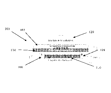
[0190]Referring now to the drawings, FIG. 1 is a schematic illustration of a
tunable
potentiometric redox-FET sensor 100 according to exemplary embodiments of the
present disclosure. The FET sensor 100 comprises a gate electrode which is
used as a
working electrode 102 and a FET amplifier 104 comprising a source terminal 106
connected to a drain terminal 108 by at least one nanowire 110. As depicted in
FIG. 1,
the FET amplifier 104 is isolated from the working electrode 102 and the
analyte
solution 120 by a chemical and electrical insulator 114. As shown in the
figure, the
analyte solution 120 is located in a well 144 defined by well walls 143. This
separation
of the working electrode 102 from the FET amplifier 104 allows the working
electrode
102 to be positioned within an analyte solution 120 in the well 144 without
any contact
between the FET amplifier 104 and the analyte solution 120. Physiochemically
isolating
the FET amplifier 104 from the analyte solution 120 by the insulator 114,
leaving only
the working electrode 102 exposed to the analyte solution 120, enhances the
specificity
of the FET sensor 100 and at least reduces undesirable FET potential drift, as
will be
described in further detail below.
[0191]In some embodiments of the present invention, the working electrode 102
is a
single working electrode connected to a voltage source 124. The working
electrode
102, in some embodiments of the present invention, comprises a noble metal
such as,
for example, gold, platinum, ruthenium, rhodium, palladium, silver, osmium,
iridium, or
similar noble metals that are very resistant to corrosion such as titanium,
tantalum
and/or carbons.
[0192]The major dimension of the exposed working electrode 102, in some
embodiments of the present invention, is approximately 200 micrometers in
length. The
major dimension is the longest dimension in a viewed plane. For example, the
major
dimension of a round wire cross section is the cross section circular
diameter. The
major dimension of a rectangular cross section of an element is the length of
the
rectangle diagonal. The major dimension of a triangular cross section of an
element is
the length of the triangle base. In other embodiments, the working electrode
102 major
dimension is 1 micron to 10,000 microns, or 100 microns to 10,000 microns, or
750
microns to 10,000 microns, or 1,500 microns to 10,000 microns, 01 2,500
microns to
27
CA 03147264 2022-01-12
WO 2021/009559 PCT/1B2020/000568
10,000 microns, or 5,000 microns to 10,000 microns, or 7,500 microns to 10,000
microns.
[0193] In some embodiments, the working electrode 102 major dimension is 1
micron to
12,000 microns. In other embodiments, the working electrode 102 major
dimension is 1
micron to 10,000 microns, or 1 micron to 7,500 microns, or 1 micron to 5,000
microns,
or 1 micron to 2,500 microns, or 1 micron to 1,000 microns, or 1 micron to 500
microns,
or 1 micron to 250 microns.
[0194] In other embodiments, the working electrode 102 major dimension is 50
microns
to about 250 microns, In other embodiments, the working electrode 102 major
dimension is 100 microns to 750 microns, or 750 microns to 5,000 microns, or
250
microns to 7,000 microns, or 2,500 microns to 3,000 microns, or 1,000 microns
to 3,000
microns, or 150 microns to 8,000 microns.
[0195] The working electrode 102 is configured to interact with an analyte 118
in the
analyte solution 120. Specifically, there is an electron transfer from the
analyte 118 to
the working electrode 102, which creates an electric field that is detected by
the FET
amplifier 104. In some embodiments of the present invention, this electron
transfer is
the result of a redox reaction between the working electrode 102 and the
analyte 118.
[0196] In some embodiments of the present invention, the redox reaction occurs
because of an enzyme-containing sensing hydrogel 116 deposited on the working
electrode 102, as shown in FIG. 3. Specifically, the sensing hydrogel 116 and
the
amount of enzyme in the hydrogel is selected such that, upon contacting an
analyte 118
in the analyte solution 120, a redox molecule is produced resulting in a shift
of the
working electrode potential.
[0197] As defined herein, a "hydrogel" is a three-dimensional fibrous network
containing
at least 20%, or at least 50%, or at least 80%, and up to about 99.99 % (by
mass)
water. A hydrogel can be regarded as a material which is mostly water, yet
behaves
like a solid or semi-solid due to a three-dimensional crosslinked solid-like
network,
made of natural and/or synthetic polymeric chains, within the liquid
dispersing medium.
According to some embodiments of the present disclosure, a hydrogel may
contain
polymeric chains of various lengths and chemical compositions depending on the
precursors used for preparing it. The polymeric chains can be made of
monomers,
28
CA 03147264 2022-01-12
WO 2021/009559 PCT/IB2020/000568
oligomers, block-polymeric units, which are inter-connected (crosslinked) by
chemical
bonds (covalent, hydrogen and ionic/complex/metallic bonds, typically covalent
bonds.)
[0198] Exemplary polymers or co-polymers usable for forming the sensing
hydrogel 116
according to the present embodiments include polyacrylates,
polyhydroxyethylmethacrylate, polymethacrylates, polyacrylam ides,
polymethacrylam ides, polyvinylpyrrolidone and copolymers of any of the
foregoing.
Other examples include polyethers, polyurethanes, functional ized
poly(ethylene glycol),
redox hydrogel (such as Os-complex based redox hydrogel), and macromers.
[0199] In some embodiments of the present invention, the sensing hydrogel 116
is
adhered to the working electrode 102 via an optional adhesive layer (not
shown). Some
examples of adhesive layers include, but are not limited to, polyurethane,
self-
assembled monolayers, or combinations thereof.
[0200]The sensing hydrogel 116, in some embodiments of the present invention,
includes at least one type of enzyme 128 that interacts with a specific
corresponding
analyte 118 to be sensed in the analyte solution 120. For example, in some
embodiments of the present invention, the enzyme within the sensing hydrogel
116
includes glucose oxidase, lactate oxidase, cholesterol oxidase, pyruvate
oxidase,
Glycerol oxidase, Alcohol oxidase, Glutaminase oxidase, L-glutamate oxidase,
Xanthine
oxidase, L-glutamate oxidase, Choline oxidase, Sarcosine oxidase and Ascorbate
oxidase or Creatininase, Creatinase, Peroxidase, Laccase, Tyrosinase or 3-
hydroxybutyrate dehydrogenase, Glucose dehydrogenase, Lactate dehydrogenase,
Alcohol dehydrogenase, Glutamate dehydrogenase. The enzyme is selected so that
the
enzyme interacts with the specific analyte 118, such as, for example, I3-d-
Glucose, L-
lactate, Glutamine, cholesterol, Glycerol, pyruvate, Ethanol L-glutamate,
Choline
Acetylcholine, I-Ascorbic acid, cortisol, Creatine, Creatinine, 2-
hydroxybutyrate or 3-
hydroxybutyrate, to form an electron transport cofactor, such as, for example,
hydrogen
peroxide, nicotinamide adenine dinucleotide (NADH), flavin adenine
dinucleotide (FAD)
and flavin mononucleotide (FMN) and quinone cofactors. The cofactors may be
inorganic, such as iron¨sulfur clusters, or organometallic such as hemes.
Thus, in
these embodiments, the formation of the electron transport cofactor creates
the
electrical shift in the working electrode potential, resulting in a change the
surrounding
29
CA 03147264 2022-01-12
WO 2021/009559 PCT/IB2020/000568
electrical field that affects the FET amplifier 104. Mediators such as
ferricyanide and
ferrocene, methylene blue, phenazines, methyl violet, alizarin yellow,
Prussian blue,
thionin, azure A and C, toluidine blue and inorganic redox ions, can be added
to the
sample or immobilized on the electrode surface.
[0201] In some embodiments of the present invention, additional limiting
membrane(s)
can also be deposited on the working electrode 102 to provide control of the
diffusion
rate and/or concentration of an analyte 118. In some embodiments of the
present
invention, the limiting membranes are semi-permeable membranes 119 such as
Nafion,
Cellulose Acetate, Polypyrrole, Polyurethane, Chitosan, Poly(2-hydroxyethyl
methacrylate), HAs/poly(diallyldimethylammonium chloride) (PDDA) and
poly(styrene
sulfonate) (PSS)/PDDA . These semi-permeable membranes 119 can also diminish
detection of interfering species such as, for example, uric acid, lactic acid,
ascorbic acid,
acetaminophen and oxygen.
[0202] In some embodiments of the present invention, an antifouling layer such
as
cellulose acetate biocides embedded in a copolymer matrix, polymers containing
phosphorylcholine (PC)-substituted methacrylate units, antimicrobial N-
halamine
polymer, fluoroalkyl diol-containing polyurethanes, poly(ether) grafted
poly(urethanes),
and plasma polymers of hexamethyldisiloxane/02, epoxy resins, Nafion,
polypeptides,
poly(ethylene glycol PEG), polyglycerol (PG), polysaccharides, polyoxazoline,
poly(propylene sulfoxide), 2-Methacryloy-loxyethyl Phosphorylcholine (MPG),
poly(phosphoester), vinylpyrrolidone, poly(vinyl alcohol) (PVA) and
zwitterionic
polymers such as phosphorylcholine, poly (carboxy-betaine acrylamide) (pCBAA)
and
sulfobetaine or carboxybetaine polymers can be used to prevent clogging and
disruption
of analyte diffusion into the sensing hydrogel 116.
[0203] Turning back to FIG. 1, the FET amplifier 104 includes a source
terminal 106 and
a drain terminal 108 connected by at least one nanowire 110. In proximity to
the electric
field of the working electrode 102, there is a continuous flow of current from
the source
terminal 106 to the drain terminal 108 across the at least one nanowire 110.
However,
changes in the surrounding electrical field by, for example, redox species
produced by
enzymatic redox reaction of bioanalyte by enzymes 128 contained in the sensing
hydrogel 116 on top of the working electrode 102 and in contact with the semi-
CA 03147264 2022-01-12
WO 2021/009559 PCT/1B2020/000568
permeable membrane 119 and with the analyte 118, may result in an increase or
a
decrease in the electric current flowing across the at least one nanowire 110.
[0204] In some embodiments of the present invention, a plurality of nanowires
may be
used. When a plurality of nanowires is employed, the nanowires are, in some
embodiments of the present invention, arranged in an array. For example, the
nanowires can be arranged generally parallel to each other. In some
embodiments of
the present invention, the FET amplifier may include from 1 nanowire to 100
nanowires,
or from 1 nanowire to 90 nanowires, or from 1 nanowire to 90 or from 1
nanowire to 75
nanowires, or from 1 nanowire to 60 nanowires, or from 1 nanowire to 45
nanowires, or
from 1 nanowire to 25 nanowires, or from 1 nanowire to 10 nanowires, or from 1
nanowire to 5 nanowires.
[0205] In some embodiments of the present invention, the FET amplifier may
include
from 5 nanowires to 100 nanowires, or from 15 nanowires to 100 nanowires, or
from 30
nanowires to 100 nanowires, or from 40 nanowires to 100 nanowires, or from 55
nanowires to 100 nanowires, or from 70 nanowires to 100 nanowires, or from 85
nanowires to 100 nanowires, or from 95 nanowires to 100 nanowires.
[0206] In some embodiments of the present invention, the FET amplifier may
include
from 15 nanowires to 65 nanowires, or from 2 nanowires to 7 nanowires, or from
10
nanowires to 15 nanowires, or from 12 nanowires to 25 nanowires, or from 35
nanowires to 55 nanowires.
[0207] In some embodiments of the present invention, the at least one nanowire
110
has a circular cross section with an average diameter of from 1 nanometer to
500
nanometers, or from 50 nanometers to 500 nanometers, or from 150 nanometers to
500
nanometers, or from 200 nanometers to 500 nanometers, or from 250 nanometers
to
500 nanometers, or from 375 nanometers to 500 nanometers, or from 450
nanometers
to 500 nanometers.
[0208] In some embodiments, the average diameter of the circular cross section
is
from 1 nanometer to 450 nanometers, or from 1 nanometer to 400 nanometers, or
from
1 nanometer to 300 nanometers, or from 1 nanometers to 250 nanometers, or from
1
nanometer to 200 nanometers, or from 1 nanometer to 150 nanometers, or from 1
nanometer to 100 nanometers, or from 1 nanometer to 50 nanometers.
31
CA 03147264 2022-01-12
WO 2021/009559 PCT/1B2020/000568
[0209] In some embodiments, the average diameter of the circular cross section
is from
nanometers to 50 nanometers, or from 150 nanometers to 400 nanometers, or from
50 nanometers to 300 nanometers, or from 100 nanometers to 250 nanometers, or
from
200 nanometers to 250 nanometers, or from 100 nanometers to 150 nanometers, or
from 400 nanometers to 450 nanometers, or from 350 nanometers to 450
nanometers.
[0210] In some embodiments of the present invention, the at least one nanowire
110
may have a non-circular cross-section. For example, the cross-section of the
at least
one nanowire 110 may have any arbitrary shape, including, but not limited to,
circular,
square, rectangular, elliptical and tubular. In some embodiments of the
present
invention, the at least one nanowire 110 may have a regular or irregular
shaped cross-
section. FIG. 2 depicts some exemplary cross-sections of the at least one
nanowire
110 according to embodiments of the present disclosure. For example, the
nanowires
may include, but are not limited to, oval 111, semi-oval 113, rectangular 115,
hexagonal
117 or trapezoidal 119.
[0211] In some embodiments of the present invention, the at least one nanowire
110
has a non-circular cross-sectional major dimension of 5 nanometers to 1000
nanometers, or 25 nanometers to 1000 nanometers, or 50 nanometers to 1000
nanometers, or 75 nanometers to 1000 nanometers, or 100 nanometers to 1000
nanometers, or 150 nanometers to 1000 nanometers, or 200 nanometers to 1000
nanometers, or 300 nanometers to 1000 nanometers, or 500 nanometers to 1000
nanometers, or 700 nanometers to 1000 nanometers, or 800 nanometers to 1000
nanometers, or 900 nanometers to 1000 nanometers.
[0212] In some embodiments, the at least one nanowire 110 has a non-circular
major
dimension of 5 nanometers to 900 nanometers, or 5 nanometers to 800
nanometers, or
5 nanometers to 700 nanometers, or 5 nanometers to 600 nanometers, or 5
nanometers to 500 nanometers, or 5 nanometers to 400 nanometers, or 5
nanometers
to 300 nanometers, or 5 nanometers to 200 nanometers, or 5 nanometers to 150
nanometers, or 5 nanometers to 100 nanometers, or 5 nanometers to 50
nanometers,
or 5 nanometers to 25 nanometers, or 5 nanometers to 10 nanometers.
[0213] In some embodiments, the at least one nanowire 110 has a non-circular
major
dimension of 10 nanometers to 100 nanometers, or 25 nanometers to 75
nanometers,
32
CA 03147264 2022-01-12
WO 2021/009559 PCT/1B2020/000568
or 250 nanometers to 750 nanometers, or 300 nanometers to 500 nanometers, or
100
nanometers to 400 nanometers, or 50 nanometers to 150 nanometers.
[0214] In some embodiments of the present invention, the at least one nanowire
110
has a length in the range of 1 micron to 500 microns. As defined herein, a
length is a
dimension of the at least one nanowire extending from a first end connected to
the
source terminal 106 to a second end connected to the drain terminal 108. In
some
embodiments of the present invention, the at least one nanowire 110 has a
length in the
range of 10 microns to 500 microns, or 50 microns to 500 microns, or 100
microns to
500 microns, or 150 microns to 500 microns, 01 200 microns to 500 microns, 01
250
microns to 500 microns, or 300 microns to 500 microns, or 400 microns to 500
microns.
[0215] In some embodiments of the present invention, the at least one nanowire
110
has a length in the range of 1 micron to 400 microns, or 1 micron to 300
microns, or 1
micron to 250 microns, or 1 micron to 200 microns, or 1 micron to 100 microns,
or 1
micron to 50 microns, or 1 micron to 25 microns, or 1 micron to 10 microns.
[0216] In some embodiments of the present invention, the at least one nanowire
110
has a length in the range of 10 microns to 50 microns, or 50 microns to 150
microns, or
25 microns to 100 microns, or 300 microns to 400 microns, or 75 microns to 200
microns, or 5 microns to 75 microns.
[0217] To increase electrical field sensitivity, the FET amplifier 104, in
some
embodiments of the present disclosure, includes silicon nanowires (SiNVV). In
some
embodiments of the present disclosure, the SiNWs respond to minor changes in
the
surrounding electrical field because of their significantly high surface area
to volume
ratio. For example, assuming a half cylinder shaped nanowire, wherein the flat
portion
of the nanowire is in contact with a substrate, the half cylinder radius, R,
is 50
nanometers (nm), and the nanowire length, L, is 10 microns, that is, 10,000
nanometers. The half cylinder nanowire volume is V=Pi/2 * R2* L and the half
cylinder
surface area is S=2 * Pi/2 * R * L. The surface area to volume ratio is Ratio
(Surface
area / Volume) = 2 / R = 1/25 = 0.04 nm-1.
[0218] In another example, assuming a nanowire with a square-shaped cross
section,
wherein the square side length, SL, is 50 nm, and the nanowire length, L, is
10 microns,
that is, 10,000 nm. The nanowire volume is V= SL2* L and the nanowire surface
area
33
CA 03147264 2022-01-12
WO 2021/009559 PCT/1B2020/000568
not in contact with the substrate, that is three faces of the rectangular
element, is S= 3*
SL * L. The surface area to volume ratio is Ratio (Surface area / Volume) = 3
/ SL =
3/50 = 0.06 nm-1.
[0219] In an embodiment, the surface area to volume ratio (Surface area /
Volume) is
smaller than 1.000 nm-1, or smaller than 0.800 nm-1, or smaller than 0.500 nm-
1, or
smaller than 0.250 nm-1, or smaller than 0.100 nm-1, or smaller than 0.080 nm-
1, or
smaller than 0.040 nm-1, or smaller than 0.020 nm-1, or smaller than 0.010 nm-
1, or
smaller than 0.005 nm-1, or smaller than 0.003 nm-1, or smaller than 0.002 nm-
1. Thus,
changes in the source-drain electric current (Isd) flow occur with minimal
losses,
providing superior sensor sensitivity.
[0220] In some embodiments of the present invention, the at least one nanowire
110
may by suspended above the substrate, as depicted in FIG. 2.
[0221] In some embodiments of the present invention, unlike typical FET
sensors, the at
least one nanowire 110 of the current FET sensor 100 are not in contact with
the
analyte 118, as will be described in further detail below, providing numerous
performance advantages, as well as flexibility of the system design. In some
embodiments of the present invention, the surfaces of the at least one
nanowire 110 are
chemically passivated. In some embodiments of the present invention, the
surfaces of
the at least one nanowire 110 are chemically passivated and reduce electrical
noise
resulting from the analyte solution 120. In other embodiments, the at least
one
nanowire is encapsulated. In other embodiments, the at least one nanowire is
encapsulated and is electrically and chemically isolated and protected from
the
environment or solution. In other embodiments, the at least one nanowire 110
is
encapsulated with a coating of metal oxides, polymers and/or other insulators.
In some
embodiments, encapsulation of the at least one nanowire 110 results in
separation of
the signal of the working electrode 102 and by-signals which may occur from
direct
contact of the analyte 118 with the at least one nanowire 110, as well as
chemical
modification of the sensitive surface of the at least one nanowire 110. Also,
by virtue of
encapsulating the at least one nanowire 110 in a stacked configuration, the
working
electrode 120 can be placed on top of the at least one nanowire 110, allowing
for
reduction in form factor, as shown in FIG. 9 and described below.
34
CA 03147264 2022-01-12
WO 2021/009559 PCT/IB2020/000568
[0222] In an embodiment, the encapsulation is achieved by covering the at
least one
nanowire with an insulator. In an embodiment, the at least one covered
nanowire is
embedded within an insulator.
[0223]As shown in FIG. 1, in some embodiments of the present invention, the
FET
sensor 100 further includes a back gate electrode 126 which allows for tuning
of the
voltage applied to the working electrode 102. The back gate electrode 126, in
this
embodiment, is a silicon based electrode. As shown in FIG. 1, the back gate
electrode
126 is separated from the FET amplifier 104 by a dielectric oxide layer 130,
which is
positioned below, and provides support to, the FET amplifier 104. Selectivity
of the FET
sensor 104 can be tuned using the back gate electrode 126 to specifically
sense
different redox species by applying different voltage settings to the working
electrode
102. Furthermore, physiochemically isolating the back gate electrode 126 from
the
analyte solution 120 by the dielectric oxide layer 130 further enhances
specificity of the
FET sensor 100 and eliminates undesirable redox potential drift.
[0224] FIGS. 4-7 depict the general mechanism of action of the FET sensor 100,
in
some embodiments of the present invention. Specifically, interaction of a
redox species
with the disclosed device forms a specific work function (WF), in units of eV,
with
respect to the working electrode 102. This leads to one of three possible
outcomes,
depending on the working electrode initial potential bias. The first possible
outcome
occurs when the WF and applied working electrode potential are equal (4)WF =
OWE).
Here, the overall electric potential will not change, resulting in no change
to the adjacent
FET Isd.
[0225] The second possible outcome occurs when the WF is higher than the
applied
working electrode potential (4)WF > OWE). In this situation, the overall
electric potential
will add up, resulting in reduced Isd in a P-type semiconductor, and increased
lsd in an
N-type semiconductor. FIGS. 4-5 depict the second scenario in which the Isd is
reduced in the P-type semiconductor¨i.e., the at least one nanowire 110. In
this
configuration, analyte A leads to positive polarization of the working
electrode, resulting
in depletion of free charge carriers (+) at the adjacent P-type silicon
nanowires 110,
thereby decreasing the electric current flowing through the drain terminal
108. This
decrease in electric current is shown in the graph of FIG. 5.
CA 03147264 2022-01-12
WO 2021/009559 PCT/1B2020/000568
[0226]The third possible outcome occurs when the WF is lower than the applied
working electrode potential ((IMF < 4)WE). In this situation, the overall
electric potential
will represent the difference between working electrode 102 and WF, resulting
in
increased Isd in a P-type semiconductor, and reduced Isd in an N-type
semiconductor.
FIGS. 6-7 depicts this third scenario in which the Isd is increased in the P-
type
semiconductor¨i.e., the silicon nanowire 110. In this configuration, the
analyte B
causes a negative polarization of the working electrode 102, resulting in an
accumulation of free charge carriers (+) at the adjacent silicon nanowires
110, thereby
increasing the electric current flowing through the drain terminal 108. This
increase in
electric current is shown in the graph of FIG. 7.
(0227] The disclosed setup of the FET sensor 100, as noted before, has
superior sensor
sensitivity, in part due to the use of silicon nanowires. While commercially
available
sensors rely on amperometric measurement, where there is a need to collect a
sufficient number of electrons at the working electrode to provide an
electrical current
signal that is above the electrical noise level. Furthermore, commercially
available
sensors typically require at least two electrodes in contact with the analyte
solution,
which results in increased electrical noise and, also increases the sensor's
dimensions.
For example, typical commercially available sensors are approximately 10 mm in
length.
In contrast, in the silicon nanowire-sensitive FET sensor 100, a small
potentiometric
change to the working electrode 102 generates a considerable current elevation
in the
adjacent FET amplifier 104. Because of this increased current elevation, as
compared
to amperometric sensors, in some embodiments of the present invention, the FET
sensor 100 may have a miniaturized footprint of about 0.0025 mm2 (0.05 x 0.05
mm).
In other embodiments, the FET sensor 100 has a miniaturized footprint of
0.00005 mm2
to 0.005 mm2, or 0.00006 mm2 to 0.005 mm2, or 0.0001 mm2 to 0.005 mm2, or
0.0005
mm2 to 0.005 mm2, or 0.001 mm2 to 0.005 mm2.
[0228] In other embodiments, the FET sensor 100 may have a miniaturized
footprint of
0.00005 mm2 to 0.001 mm2, or 0.00005 mm2 to 0.0005 mm2, or 0.00005 mm2 to
0.0001
mm2, or 0.00005 mm2 to 0.00006 mm2.
[0229] In other embodiments, the FET sensor 100 may have a miniaturized
footprint of
0.0001 to 0.001 mm2, or 0.0025 to 0.0005 mm2, or 0.0006 to 0.001 mm2.
36
CA 03147264 2022-01-12
WO 2021/009559 PCT/1B2020/000568
[0230]In some embodiments, the FET sensor 100 has a miniaturized major length
of
length of about 0.2 mm. In other embodiments, the FET sensor 100 has a
miniaturized
major length of 0.1 mm to 1.5 mm, 0r0.1 mm to 1.3 mm, 0r0.1 mm to 1.1 mm,
0r0.1
mm to 0.9 mm, or 0.1 mm to 0.7 mm, or 0.1 mm to 0.5 mm, 01 0.1 mm to 0.3 mm.
[0231]In some embodiments, the FET sensor 100 has a miniaturized major length
of
0.3 mm to 1.5 mm, or 0.5 mm to 1.5 mm, or 0.7 mm to 1.5 mm, 01 0.9 mm to 1.5
mm, or
1.1 mm to 1.5 mm, or 1.3 mm to 1.5 mm.
[0232]In other embodiments, the FET sensor 100 has a miniaturized major length
of 0.3
mm to 1.1 mm, or 0.7 mm to 0.9 mm, or 0.9 mm to 1.3 mm, or 0.5 mm to 1.1 mm,
01 0.3
mm to 0.5 mm, or 0.5 mm to 1.1 mm, or 0.7 mm to 1.3 mm. The major length of
the
FET sensor 100 allows the FET sensor 100 to be placed in compact devices, such
as
microprobes or minimally-invasive microprobes aimed at sensing multiple
different
metabolites and other chemicals in the interstitial fluid. The miniaturized
size of the
current FET sensor 100 can be seen in FIG. 8.
[0233]FIG. 9 depicts a compact, layered design, of a tunable potentiometric
redox-FET
sensor 200, in some embodiments of the present invention, with a reduced form
factor
due to the covering of the at least one nanowire 210 with the chemical and
electrical
insulator 214. In this embodiment, at least one silicon nanowire (SiNVV) 210
is
connected to a source terminal and a drain terminal to form the FET amplifier
204,
similar to FET amplifier 104. However, in this embodiment, the FET amplifier
204,
working electrode 202 and chemical and electrical insulator 214 are in a
stacked
configuration. Specifically, the working electrode 202 is stacked over the
insulator 214,
which is stacked over the FET amplifier 204. Insulator 214 separates the FET
amplifier
204 from the working electrode 202 and from the analyte solution 220 in the
well 244.
The well is defined by polymeric well walls 243, as shown in the figure.
Additionally, the
FET sensor 200, in this embodiment, the back gate electrode 226 and the
dielectric
oxide layer 230 are positioned under both the FET amplifier 204, as shown in
FIG. 9,
providing a more compact sensor design and reduction in form factor.
Calibration of the FET Sensor
37
CA 03147264 2022-01-12
WO 2021/009559 PCT/1B2020/000568
[0234] One objective of the calibration process in the present invention is to
identify a
voltage value or voltage value range in which the performance of the working
electrode
will be robust and sufficiently sensitive. In some cases, the calibration
process also
identifies the voltage value or voltage value range of the back gate electrode
that will
support this performance level of the working electrode.
[0235] The calibration process, in some embodiments of the present invention,
may be
required for various reasons. For example, in some instances, where multiple
FET
sensors are being used, there may be differences between devices from
different
manufacturing lots. Also, within the same manufacturing lot there may be
differences in
sensor performance. In other instances, calibration may be required when
working with
multiple sensors whose performance curves have similar shapes but may be
shifted in
some manner. Furthermore, in some cases, sensor performance may drift due to
natural material degradation or to environmental or external factors, which
can be
accounted for by calibration.
[0236] In one aspect of the present invention, a robust sensor performance
results in the
sensor being capable of identifying a target analyte, repeatedly and
consistently and is
insensitive to other materials and noise. In another aspect of the present
invention, the
calibration process is based on identifying a singularity point in the
performance graph
of a sensor for a given analyte. A singularity point may be a voltage value or
small
voltage range in which the sensor's response to a specific analyte (i.e.,
change in lsd
current) is minimized or becomes unnoticeable.
[0237] In some embodiments of the present invention, the sensor's sensitivity
to a
specific analyte will increase as the voltage level is increased or reduced
from the
voltage value at the singularity point. In an example, a singularity point can
be identified
as a peak or valley in the response graph. To the sides of the peak or valley,
the
response is highly sensitive. This can be seen for example, in an analysis of
the first
derivative of the response graph. At the peak or valley, the value of the
first derivative
is zero. To the sides of the peak or valley, the absolute value of the first
derivative is
greater than zero. That is, the sensor's response is enhanced. Thus, for high
sensitivity, the working electrode voltage will be preferentially set at a
value that is equal
to the singularity point voltage +/- an offset voltage level.
38
CA 03147264 2022-01-12
WO 2021/009559 PCT/IB2020/000568
[0238] In an exemplary embodiment, the calibration process includes two modes.
A
"coarse calibration mode," in which identification of the singularity point
voltage is
achieved by changing the back gate voltage for a given working electrode
voltage, and
a "fine-tuning calibration mode," in which identification of the singularity
point voltage is
achieved by changing the working electrode voltage, for a given, fixed back
gate
voltage. However, there may be interactions between the two modes, such that
the
sequence of the calibration modes is significant. The final determination of
the
singularity point voltage should be done with the fine-tuning mode, for a
given, fixed
back gate voltage,
[0239] Once the singularity point potential has been determined, an offset
voltage is
applied to the back-gate voltage and to the working electrode voltage. The
offset
voltage levels and direction is also analyte specific and is determined
empirically
through experimentation. For example, in one embodiment of the present
invention, in
the case of hydrogen peroxide sensing, a typical working electrode offset
would be
approximately +1- 0.2 to 0.5 v and a typical back gate offset would be
approximately +1-
0.5 to 1 v. These offsets will provide robustness and sensitivity to sensor
performance,
that is, a consistent high response to the desired analyte.
[0240] FIGS. 10-11 provide an example of the way proper tuning of a sensor
provides
filtering of possibly interfering substances or chemical species so that only
the
substance of interest is being detected in an analyte solution, in some
embodiments of
the present invention. Specifically, FIGS. 10-11, in one example, demonstrate
how to
prevent interference from ascorbic acid redox. Metgraphs of FIG. 10 and FIG.
11 show
the Isd electric current recordings of the same device when introduced to 1 mM
hydrogen peroxide and 342 uM ascorbic acid solutions. However, the back gate
voltage
(VBg) and working electrode voltage (VVVE) are different. In FIG. 10, VBg =-
1v, VWE=-
0.2. Using these settings, the presence of hydrogen peroxide leads to an
elevated
current level while the sensor's response to ascorbic acid was diminished.
[0241] FIG. 12 is a flow chart of an exemplary calibration process, in some
embodiments of the present invention. In Mode I, the back gate coarse
calibration
mode, the back gate voltage is changed, while the working electrode voltage is
held
constant. At each back gate voltage setting, the response is reviewed until a
singularity
39
CA 03147264 2022-01-12
WO 2021/009559 PCT/IB2020/000568
point is identified. The back gate working voltage is then set to a voltage
level that is
equal to the voltage level at which the singularity point is identified +1- a
voltage offset.
Once the back gate coarse calibration has been completed, fine-tuning
calibration of the
working electrode voltage may commence.
[0242] In Mode II, separated from Model in FIG. 12 by the horizontal dotted
line, the
fine-tuning calibration of the working electrode is performed by changing the
working
electrode voltage while the back gate voltage is held constant. At each
working
electrode voltage setting, the response is analyzed until a singularity point
is identified.
The working electrode voltage is then set to a voltage level that is equal to
the voltage
level at which the singularity point was identified with +1- a voltage offset.
[0243] In some cases, a partial calibration, including only the working
electrode fine
tuning calibration, may be sufficient. For example, if the sensor has been
calibrated in
the past and is due for a periodic calibration, if there is an operational
motivation to
verify the performance of a working sensor, or if there is a concern that
there is a
degradation in the functionality of the sensor components. The back gate
coarse
calibration may be applied primarily on new sensors or in situations in which
the
singularity point cannot be identified with the working electrode fine tuning
calibration
procedure.
[0244] FIG. 13 depicts a graph of a calibrated response of, in this example, a
glucose
sensor under in vitro conditions for different glucose concentrations (in
phosphate
buffer), in some embodiments of the present invention. As can be seen, the
graph is
linear for the log2 of glucose concentration with the current increasing as
the
concentration increases, indicating a normalized sensor signal.
[0245] FIG. 14 shows a graph of current (Isd) plotted against working
electrode voltage
(WE) as the working electrode voltage is swept over a range from -0.7 V to 0.7
V, in
some embodiments of the present invention. Each trace represents current
levels
recorded repeatedly by the same sensor unit as described above. In the sample
shown
in FIG. 14, current was recorded while the sensors were exposed to phosphate
buffer
(PB), such that no redox reaction occurred at the working electrode. As a
result, the
plots of current shown in FIG. 14 follow relatively smooth curves. In a
similar
experiment, current was recorded while the same sensors were exposed to a 1 mM
CA 03147264 2022-01-12
WO 2021/009559 PCT/1B2020/000568
hydrogen peroxide solution, such that a redox reaction occurred. As a result,
a variation
in the measured current was induced. As may be seen, an inflection point is
present at
an equilibrium voltage of about -0.2 V, with maximum current elevation
response at
about 0.05 V and maximum current elevation response at about -0.45 V. As a
result,
such a voltage sweep may identify -0.2 V as an inflection point, which is the
voltage
setting that reduces (e.g., tunes out) a sensor's response to hydrogen
peroxide. These
findings correlate well with exemplary discrete fixed voltage experiments, the
results of
which are shown in FIG. 15.
[0246] As can be seen in the graph, three different regimes can be observed
when the
analyte is switched between PB and hydrogen peroxide at different WE
potentials. It
can be seen from the graph that at a WE voltage of -0.2v there is negligible
net change
of the lsd in response to the introduction of hydrogen peroxide, which
correlates to the
inflection point observed in the voltage sweep experiment (Fig 15). At a WE
voltage of
approximately 0-0.1V there is a visible net lsd current elevation in response
to hydrogen
peroxide which correlates to the maximum current elevation response seen in
Fig. 15 at
0.05v. At a WE voltage of approximately -0.3v to -0.4v there is a net Isd
current
reduction in response to hydrogen peroxide.
Multi-Microprobe Sensing Chip
[0247] FIGS. 16-20 depict a multi-microprobe sensing chip 132, according to an
exemplary embodiment of the present disclosure. As can be seen in FIGS. 16-19,
the
sensing chip 132 includes at least one sensing microprobe 136 extending
outwardly
from a bridge portion 134 of the sensing chip 132. The at least one sensing
microprobe
136 has a body 140 that connects a tip of the microprobe 142 to the bridge
portion 134.
The tip 142 of the microprobe can have any shape, including, without
limitation, a
conical shape, a cylindrical shape, a tubular shape and a pyramidal shape. In
an
embodiment, the tip 142 of the at least one microprobe 136 is sharp such that
it will
form a minimally invasive skin-penetrating microprobe. In some embodiments of
the
present invention, the at least one microprobe 136 is straight, but non-
straight shapes
(e.g., a curved microprobe, a hook-shape microprobe, or a semi hook-shape
microprobe) are also contemplated. The at least one microprobe 136 can
protrude
41
CA 03147264 2022-01-12
WO 2021/009559 PCT/1B2020/000568
perpendicularly from the bridge portion 134 of the microprobe array. The at
least one
microprobe 136, in some embodiments of the present invention, has a base 138
attached to or integral with the bridge portion 134 of the sensing chip 132
with the body
140 extending away from the bridge portion 134 of the sensing chip 132. The
tip 142 is
distal to body 140, which is distal to the base 138.
(0248] The at least one microprobe 136, in some embodiments of the present
invention,
is hollow or provided with a well 144 embedded therein, and contains at least
one
opening for allowing the at least one microprobe 136 to exchange fluids with a
medium
outside the at least one microprobe 136. FIG, 20 is a magnified schematic
illustration
showing a portion of a sensing microprobe 136 with a well 144 at a distal
portion
thereof. In another embodiment of the distal well architecture, the FET
sensing element
can be situated at another environment/compartment such as embedded in a
dielectric
material which allows the sensing of the WE potential as a result of analyte
redox
activity at the well portion of the sensor.
[0249]The term "well" as used herein refers to a fluid compartment having, in
some
embodiments, a cross-sectional circular, rectangular, or oval shaped opening.
In some
embodiments, the opening is oval shaped with a major dimension of less than
0.1 mm,
0r0.3 mm, or 0.5 mm, 0r0.7 mm, or 0.9 mm, or 1.1 mm, or 1.3 mm, or 1.5 mm. In
some embodiments, the oval-shaped opening has a minor dimension that is less
than
90%, or 80%, or 70%, or 60%, or 50%, or 40%, or 30%, or 20% of the major
dimension.
[0250] In some embodiments, the opening is substantially rectangular shaped
with a
major dimension of less than 0.1 mm, 0.3 mm, 0.5 mm, 0.7 mm, 0.9 mm, 1.1 mm,
1.3
mm or 1.5 mm. In some embodiments, the substantially rectangular opening has a
minor dimension of less than 90%, or 80%, or 70%, or 60%, or 50%, or 40%, or
30% or
20% of the major dimension.
[0251] In some embodiments of the present invention, the at least one
microprobe has
an opening at the tip. In some embodiments of the present invention, the at
least one
microprobe or a portion thereof can be porous. Alternatively, the at least one
microprobe can be non-porous with only one or a few openings formed on its
body. The
at least one microprobe, in some embodiments of the present invention,
comprises a
non-degradable material.
42
CA 03147264 2022-01-12
WO 2021/009559 PCT/1B2020/000568
[0252] In some embodiments of the present invention, the diameter of the at
least one
microprobe is selected to leave a residual hole (following microprobe
insertion and
withdrawal) of less than about 1 pm, to avoid making a hole which would allow
bacteria
to enter the penetration wound. The length of the penetrating portion is, in
some
embodiments of the present invention, selected to allow the penetrating
portion to
penetrate the skin, for example, beyond the stratum corneum layer. In some
embodiments of the present invention, the length of the penetrating portion is
selected
to positioning tip in the viable epidermal layer but not in the dermal layer.
In exemplary
embodiments, the length of the penetrating portion is from 0.05 mm to 1 mm, or
from
0.05 to 0.8 mm, or from 0.05 mm to 0.75 mm, or from 0.05 mm to 0.6 mm, or from
0.05
mm to 0.5 mm, or from 0.05 mm to 0.4 mm, or 0.05 mm to 0.3 mm, or from 0.05 mm
to
0.25 mm, or from 0.05 mm to 0.15 mm.
[0253] In some embodiments of the present invention, the length of the
penetrating
portion is from 0.05 mm to 1 mm, or from 0.15 mm to 1 mm, or from 0.2 mm to 1
mm, or
from 0.35 mm to 1 mm, or from 0.45 mm to 1 mm., or from 0.5 mm to 1 mm, or
from
0.75 mm to 1 mm, or from 0.85 mm to 1 mm, or from 0.9 mm to 1 mm.
[0254] In some embodiments of the present invention, the length of the
penetrating
portion is from 0.35 mm to 0.75 mm, or from 0.55 mm to 0.65 mm, or from 0.75
mm to
0.95 mm. In other embodiments, the length of the penetrating portion is less
than 1
mm, or less than 2 mm, or less than 3 mm, or less than 4 mm, or less than 5
mm.
[0255] The sensing chip can be constructed from any of a variety of materials
including,
without limitations, metals, ceramics, semiconductors, organics, polymers and
composites.
[0256] In some embodiments of the present invention, the microprobe array
includes
microprobes of various lengths, base portion materials, body portion diameters
(i.e.
gauge), tip portion shapes, spacing between microprobes, coatings, etc.
[0257] In some embodiments of the present invention, each microprobe 136
includes a
FET sensor 100 positioned at, but not limited to the distal portion of the
microprobe 136.
A magnified schematic illustration of the FET sensor 100 positioned on the at
least one
microprobe 136 according to some embodiments of the present invention is shown
in
FIG. 20. As depicted in the figure, each microprobe 136 includes a working
electrode
43
CA 03147264 2022-01-12
WO 2021/009559 PCT/1B2020/000568
102 that is positioned at the well 144 so as to be in contact with the analyte
solution 120
that collects within it, when the microprobe 136 is immersed in an analyte.
The working
electrode 102 includes a trace 137 that extends at least a portion of the
length of the at
least one microprobe 136 to the main portion 134 of the sensing chip 132. In
some
embodiments, the working electrode 102 and the trace 137 are formed of the
same
material. In some embodiments, a portion of the working electrode 102 and/or
the trace
137 may be covered or encapsulated. As shown in FIG. 20, on the main portion
134 of
the sensing chip 132, at least one FET amplifier 104 is positioned in close
proximity to
the working electrode 102. As described above, the FET amplifier 104 includes
a
source terminal 106, a drain terminal 108, and at least one nanowire 110
connecting the
source and drain terminals 106, 108. In exemplary embodiments, each FET sensor
100
is designed to be functionalized using different analyte-specific materials,
such as a
sensing hydrogel 116 embedded with enzymes described above, in order to
achieve
multi-metabolite sensing capabilities. For example, in some embodiments of the
present invention, each FET sensor may comprise a sensing hydrogel 116
attached to
the working electrode 102 embedded in the at least one microprobe 136.
[0258] In some embodiments, the at least one microprobe 136 may each include
two
FET sensors 100. In some embodiments of the present invention, the FET sensor
100
includes more than one FET amplifier 104 detecting the electrical change in
the working
electrode 102.
[0259] In some embodiments of the present invention, the chip includes one or
more
microprobes used for calibration, which are also outwardly protruding from the
main
portion, similar to the at least one sensing microprobe. Calibration
microprobes may
have the same structure as the at least one sensing microprobe but are, in
some
embodiments of the present invention, devoid of a hydrogel containing an
enzyme or
any moiety configured to react with analytes in the analyte solution. However,
in some
embodiments of the present invention, the calibration microprobes include
hydrogels
with moieties having an affinity to a substance other than a bioanalyte.
Alternatively,
the calibration microprobes may have hydrogels with non-sensing moieties or
enzymes.
[0260] FIGS. 21-32 illustrate an exemplary method of microchip production, in
some
embodiments of the present invention. As depicted in FIG. 21, in an exemplary
44
CA 03147264 2022-01-12
WO 2021/009559 PCT/1B2020/000568
embodiment, a silicon-on-insulator (SOD wafer 148 with a buried oxide layer
150 and an
ultrathin silicon device layer (for example, <100 nm) 152 is used. The device
layer may
have, for example, a dopant concentration of 1015 - 1017 atoms/cm3.
[0261] In step 1, as depicted in FIG. 22, the silicon device layer 152 is
lithographically
patterned via e-Beam, stepper or scanner lithography or other equivalent nano-
lithography techniques. The device layer 152 may then be etched via wet
anisotropic
chemical etching or dry, plasma-based silicon etching with reactive species to
form the
at least one nanowire 110 or nanowire arrays.
[0262] In step 2, after the at least one nanowire 110 is formed, the back gate
126 is
etched, through the buried oxide layer 150, as shown in FIG. 23. Specifically,
the back
gate 126 is lithographically patterned and then etched through the buried
oxide layer
150 via photolithography, stepper or scanner lithography. The buried oxide
layer 150 is
then etched via wet isotropic chemical etching or dry, plasma based silicon
dioxide
etching with a reactive species.
[0263] In step 3, depicted in FIG. 24, photolithography, stepper or scanner
lithography is
used to lithographically pattern resist for the working electrode 102 and bond
pads 190.
Specifically, a metal stack is deposited in the lithographically patterned
resist via
evaporation, sputtering or electrodeposition. The metal stack includes an
initial layer for
adhesion and silicide formation as well as a noble metal layer for exposure to
environment. In some embodiments of the present invention, the initial layer
is one of
Titanium, Nickel or TiN.
[0264] In step 4, depicted in FIG. 25, native silicon dioxide is etched via
wet isotropic
etching or dry etching and a metal stack 194 is deposited in a
lithographically patterned
resist via evaporation, sputtering or electrodeposition to form the nanowire
contacts 196
between the metal stack and the nanowire, in this embodiment, the SiNW 110. In
some
embodiments, the metal stack 194 includes an initial layer for adhesion and
silicide
formation (Ti, Ni or TiN) a second metal layer with lower electrical
resistance (Al, AlSi,
AlSiCu, Pd, Au, Cu or Ag) and a third top layer (Ti, Al, Cr) for improved
adhesion to
following passivation layers.
[0265] In step 5, depicted in FIG. 26, the at least one nanowire contact (not
shown) may
undergo rapid thermal annealing (RTA) in an inert nitrogen or argon atmosphere
or with
CA 03147264 2022-01-12
WO 2021/009559 PCT/IB2020/000568
forming gas. The RTA-induced suicide formation results in a transformation of
the
nanowire contact into an interface volume 197.
[0266] In step 6, depicted in FIG. 27, a passivation layer 188 is deposited
for electrical
isolation via atomic layer deposition (ALD), inductively coupled plasma -
chemical vapor
deposition (ICP-CVD) or Tetraethylorthosilicate (TEOS). The passivation layer
188, in
some embodiments of the present invention, comprises one of aluminum oxide,
silicon
nitride, silicon dioxide or silicon oxynitride.
[0267] In step 7, depicted in FIG. 28, a resist is lithographically patterned
in the back of
the wafer via photolithography, stepper or scanner lithography. A back gate
handle 198
is etched with silicon via wet anisotropic silicon etching or plasma based
anisotropic
deep silicon etching (DSE).
[0268] In step 8, depicted in FIGS. 29-30, openings 174 are lithographically
patterned
on the passivation layer 188. The openings 174 are then etched through the
passivation layer 188 via isotropic wet chemical etching or plasma based dry
etching
with a reactive species to expose the working electrode 102, the back gate
electrode
126 and the at least one nanowire 110. This etching exposes the noble metal of
the at
least one nanowire 110 to the environment,
[0269] In step 9, depicted in FIG. 31, a thick, permanent photoresist 192 is
lithographically patterned via photolithography, stepper or scanner
lithography to form
the well 144. In some embodiments of the present invention, the photoresist
192 is in
the range of 5 to 50 microns. In some embodiments of the present invention,
the
photoresist 192 is formed of SU-8 or polyimide.
[0270] In step 10, depicted in FIG. 31, a resist is lithographically patterned
via
photolithography, stepper or scanner lithography to define a well 144 and well
walls 143
the at least one microprobe and the microchip. The passivation layer is then
etched via
wet chemical etching or plasma based dry etching with a reactive species. The
buried
oxide layer is also etched with wet chemical etching or plasma based dry
etching with
reactive species while the handle layer silicon is etched via plasma based
anisotropic
deep silicon etching (DSE).
[0271] Finally, in step 11, depicted in FIG. 32, the singulated microchip 132
is removed
from the silicon wafer by breaking tabs connecting the microchip 132 to the
wafer.
46
CA 03147264 2022-01-12
WO 2021/009559 PCT/1B2020/000568
[02721 FIG. 33 depicts how, in use, a microchip 132 with a single FET sensor
100 can
measure different concentrations of, for example, a chemical species over
time, in some
embodiments of the present invention. In this embodiment, the FET sensor 100
is
tuned to measure hydrogen peroxide. FIG. 33 shows the recording of current
flow from
the single FET sensor 100 over time. The measurement was done under a fixed
working electrode voltage. As can be seen from the graph, changing the
hydrogen
peroxide concentration results in a change of the current levels through the
FET
amplifier 104. Specifically, an increase in hydrogen peroxide concentration
results in a
reduction of the current level while a decrease in the hydrogen peroxide
concentration
results in an increase in the current level. For example, changing the
hydrogen
peroxide concentration from 10 pM to 1 mM reduces the current level from
approximately 150 nA to 70 nA.
[0273]FIG. 34 depicts an exemplary setup of a multi-microprobe sensing chip
132
configured for monitoring, in this example, glucose, lactate and ascorbic acid
(AA) in an
analyte solution, in some embodiments of the present invention. In this
embodiment,
the multi-microprobe sensing chip includes six microprobes, each including an
FET
sensor. The exemplary embodiments include a specific discussion of devices
configured to detect glucose, lactate and ascorbic acid, but it will be
apparent to those
of skill in the art that devices can be configured to detect other analytes
(i.e., 13-d-
Glucose, L-lactate, Glutamine, cholesterol, Glycerol, pyruvate, Ethanol L-
glutamate,
Choline Acetylcholine, I-Ascorbic acid, cortisol, Creatine, Creatinine, 2-
hydroxybutyrate
or 3-hydroxybutyrate) through the use of enzymes (i.e., glucose oxidase,
lactate
oxidase, cholesterol oxidase, pyruvate oxidase, Glycerol oxidase, Alcohol
oxidase,
Glutaminase oxidase, L-glutamate oxidase, Xanthine oxidase, L-glutamate
oxidase,
Choline oxidase, Sarcosine oxidase and Ascorbate oxidase or creatininase,
Creatinase,
Peroxidase, Laccase, Tyrosinase or 3-hydroxybutyrate dehydrogenase, Glucose
dehydrogenase, Lactate dehydrogenase, Alcohol dehydrogenase, Glutamate
dehydroge) for such other analytes as enzyme substrates without departing from
the
broader principles described herein.
(0274] Specifically, the multi-microprobe sensing microchip 132 includes a
first
microprobe 154 having a first FET sensor 156. The working electrode of the
first FET
47
CA 03147264 2022-01-12
WO 2021/009559 PCT/IB2020/000568
sensor 156, in this embodiment, is embedded with a GOX-containing hydrogel.
The
GOX reacts with glucose in the analyte solution to produce hydrogen peroxide
(H202).
A second microprobe 158 of the microchip 132 includes a second FET sensor 160.
A
working electrode of the second FET sensor 160, in this embodiment, is
embedded with
a LOX-containing hydrogel. The LOX reacts with lactate in the analyte solution
to
produce H202. A third microprobe 162 of the multi-microprobe sensing chip 132
includes a third FET sensor 164. However, the working electrode of the third
FET
sensor 164 is embedded with a hydrogel devoid of any enzymes. Thus, the third
FET
sensor 164 detects all background analytes within the analyte solution to
allow for
correction of the measurements from the first and second FET sensors 156, 160.
In this
embodiment, each of the first, second and third FET sensors 156, 160, 164 have
the
same voltage setting so that the third FET sensor 164 acts as a blank sensor
to
compensate for background noise. Thus, by deducting the third FET sensor
output
from the first FET sensor output, amounts of glucose within the analyte
solution can be
calculated. Similarly, by deducting the third FET sensor output from the
second FET
sensor output, amounts of lactate within the analyte solution can be
calculated.
[0275] Turning to the fourth microprobe 166 of the multi-microprobe sensing
chip 132, a
fourth FET sensor 168 positioned thereon is designated, in this embodiment as
an
ascorbic acid sensor. The working electrode of the fourth FET sensor 166, in
this
embodiment, is embedded with a hydrogel that is devoid of enzymes, while its
voltage is
tuned to maximize ascorbic acid (AA) sensing. For example, the back
gate/working
electrode voltage may be set to more negative values. A fifth microprobe 170
of the
multi-microprobe sensing chip 132 includes a fifth FET sensor 172. The working
electrode of the fifth FET sensor 172, in this embodiment, is embedded with
ascorbic
acid oxidase (AAOX), which does not produce hydrogen peroxide, only
dehydroascorbic
acid and water. Thus, the AAOX is used to eliminate AA and by deducting the
fifth FET
sensor output from the fourth sensor output, AA concentration can be
calculated. A sixth
microprobe 173 of the multi-needle sensing chip 132 includes a sixth FET
sensor 175.
The working electrode of the sixth FET sensor 175, in this embodiment, is
embedded
with an ion-specific ionophore membrane to allow the measurement of specific
ion such
as Beauvericin (Ca2+, Ba2+), Calcimycine or A23187 (Mn2+, Ca2+, Mg2+),
48
CA 03147264 2022-01-12
WO 2021/009559 PCT/IB2020/000568
Cezomycin, Carbonyl cyanide m-chlorophenyl hydrazone (CCCP) (H+), Enniatin
(ammonium), ramicidin A (H+, Na+, K+),Ionomycin (Ca2+), Lasalocid (K+, Na+,
Ca2+,
Mg2+), Monensin (Na+, H+),Nigericin (K+, H+, Pb2+), Nonactin (ammonium
ionophore
I), Salinomycin (K+), Tetronasin, Valinomycin (potassium ionophore I),
Narasin, or
combinations thereof.
Microprobe Sensing System
[0276] In some embodiments of the present invention, depicted in FIGS. 35-36,
the
multi-microprobe sensing chip 132 is incorporated into a sensing system 180.
The
sensing system 180, in some embodiments of the present invention, is
configured as a
patch or removable implant that allows for monitoring presence, absence or
amounts of
multiple bioanalytes. As depicted in FIG. 35, in some embodiments of the
present
invention, the sensing system 180 comprises a sensor patch 182 having a skin
contact
surface 184 for contacting the skin of a subject (human or animal). The sensor
patch
182, in some embodiments of the present invention, is configured to hold the
multi-
microprobe sensing chip 132 such that one or more sensing microprobes 136
outwardly
protrude from the skin contacting surface. In exemplary embodiments, the at
least one
microprobe 136 can protrude perpendicularly from the surface 184 of the sensor
patch
182, or at an acute angle from the surface 184. In some embodiments of the
present
invention, a circuit is attached to the sensor patch 182. In some embodiments
of the
present invention, the circuit is positioned at an opposite side of the
substrate relative to
the microprobes.
(0277] FIG. 36 depicts a sensor patch 182, according to an exemplary
embodiment of
the present disclosure. The sensor patch surface 184 is, in some embodiments
of the
present invention, an adherent surface, allowing the substrate to be attached
to the
skin. For example, the surface can comprise, or be coated with, a skin
adherent
material. In some embodiments of the present invention, the sensor patch 182
also
contains a substance selected for preventing or reducing skin irritations such
as, but not
limited to, pruritus, flush, rash, pain, eczema and skin inflammation. In some
embodiments of the present invention, the sensor patch 182 is flexible. For
example,
the sensor patch 182 can be made, at least in part, of a woven fabric, a
nonwoven
49
CA 03147264 2022-01-12
WO 2021/009559 PCT/1B2020/000568
fabric, a plastic film or the like. Portions of the sensor patch 182 are made,
for example,
of elastomeric polymer. Suitable elastomeric polymer substrate materials are
generally
selected based upon their compatibility with the manufacturing process (soft
lithography, stereo lithography and three-dimensional jet printing, etc.).
Given the
tremendous diversity of polymer chemistries, precursors, synthetic methods,
reaction
conditions, and potential additives, there is a large number of materials that
are
contemplated for use. Representative examples of elastomeric polymers include,
without limitation, polydimethylsiloxane (PDMS), polyisoprene, polybutadiene,
polychloroprene, polyisobutylene, poly(styrene-butadiene-styrene),
polyurethanes and
silicones. Polymers which are generally non-elastomeric are also contemplated.
Representative examples of such polymers include, without limitation, PMMA and
polycarbonate.
[0278]Also contemplated are embodiments in which the sensor patch 182 is made
of
two or more materials. For example, a portion of the sensor patch 182 can be
made
from a woven or nonwoven fabric, or film, that is, in some embodiments of the
present
invention, coated with a skin adherent material, while another portion serves
as a
microfluidic interface, wherein microprobes 136, are formed on or integral
with
microfluidic interface. Microfluidic interface can be made more rigid than the
fabric or
film.
[0279]The lateral dimensions of sensor patch 182 may vary, depending on the
size of
the organ of the subject that receives surface 14. A typical lateral diameter
of sensor
patch 182 is, without limitation, from about 10 mm to about 50 mm.
[0280]As noted above, in some embodiments of the present invention, the FET
sensor
response to a redox species in an analyte solution can be processed and
measured by,
for example, the circuit. In some embodiments of the present invention, the
circuit can
be constructed, for example, to measure the current passing through the drain
terminal
of the FET amplifier.
[0281]The FET amplifiers positioned on the sensing chip are, in some
embodiments of
the present invention, connected directly or indirectly to the circuit. The
circuit applies
voltage to the FET amplifier. The circuit typically includes a power source
and a
voltmeter or amperemeter. When the reaction between the sensing hydrogel and
the
CA 03147264 2022-01-12
WO 2021/009559 PCT/1B2020/000568
analytes in solution is a redox reaction, the circuit, in some embodiments of
the present
invention, is configured for controlling the voltage settings of the back gate
to the
working electrode.
[0282] It is appreciated that certain features of the disclosure, which are,
for clarity,
described in the context of separate embodiments, may also be provided in a
single
embodiment. Conversely, various features of the disclosure, which are, for
brevity,
described in the context of a single embodiment, may also be provided
separately or in
any suitable sub combination or as suitable in any other described embodiment
of the
disclosure. Certain features described in the context of various embodiments
are not
considered essential features of these embodiments, unless the embodiment is
inoperative without those elements.
51